應用於X頻帶EER發射器之互補金氧半E類功率放大器設計
78
0
0
全文
(2) 應用於 X 頻帶 EER 發射器之互補金氧半 E 類功率放大器設計. CMOS Class-E Power Amplifier Design for X-Band EER Transmitter 研 究 生:王磊中. Student. 指導教授:溫瓌岸 博士. Advisor. 共同指導:溫文燊 博士. Co-Advisor. :Roger Randolph Wang :Dr. Kuei-Ann Wen :Dr. Wen-Shen Wuen. 國 立 交 通 大 學 電子工程學系 電子研究所碩士班 碩 士 論 文. A Thesis Submitted to Department of Electronics Engineering & Institute of Electronics College of Electrical & Computer Engineering National Chiao Tung University in Partial Fulfillment of the Requirements for the Degree of Master In Electronic Engineering. 中 華 民 國 九 十 七 年 六 月.
(3) 應用於 X 頻帶 EER 發射器之互補金氧半 E 類功率放大器設計 學生:王磊中. 指導教授:溫瓌岸 博士 共同指導:溫文燊 博士. 國立交通大學電子工程學系 電子研究所碩士班. 摘. 要. 本文提出了第一個操作在 X 頻帶並且完全整合在單一晶片上的 CMOS E 類功 率放大器。此 E 類功率放大器使用了 0.18-μm CMOS 製程並且利用了注射式鎖定 之技巧以達到 X 頻帶的操作。量测結果顯示此 E 類放大器操作在 8.41GHz 時,可 達到 10.75dBm 的輸出功率和 17%的功率增加效率,以及 20dB 之增益。在設計的 頻帶內,8.35GHz~8.45GHz,功率增加效率仍然可以維持在 14%以上。且為了增 加上述電路於 EER 發射器中調變的準確度。本文提出了一個補償 AM/PM 失真之 技巧以達到 IEEE 802.11a 寬頻 OFDM 資料流傳送之線性度與頻寬規格。模擬結 果顯示,在訊號頻寬 20MHz,以及 64-QAM 調變,且應用補償技術的情況下。本 文所提出的 E 類功率放大器在中心頻率為 8.4GHZ 時可以-25.2dB 之 EVM 達到 IEEE802.11a 之線性度規格要求並且同時傳送 9dBm 之平均輸出功率與 15%之功率 增加效率。. I.
(4) CMOS Class-E Power Amplifier Design for X-Band EER Transmitter Student:Roger Randolph Wang. Advisor:Dr. Kuei-Ann Wen Co-Advisor:Dr. Wen-Shen Wuen. Department of Electronics Engineering Institute of Electronics National Chiao-Tung University. ABSTRACT A first X-Band fully integrated Class-E power amplifier is proposed in this thesis and fabricated in 0.18-µm CMOS technology. Injection locking technique is applied to help the reach of the X-Band operation. Measurement results show that the proposed Class-E power amplifier could achieve 17% power added efficiency (PAE) and delivering an output power of 10.75dBm with gain 20dB at 8.41 GHz. Also, the PAE is over 14% over the frequency range 8.35 GHz to 8.45 GHz. In order to improve the modulation accuracy of the proposed circuit under the EER transmitter, a compensation technique for AM/PM distortion is proposed to achieve the linearity requirements of IEEE 802.11a data stream broadband OFDM transmission. Simulation results show that with compensation technique, 20MHz signal bandwidth and 64-QAM modulation, the proposed Class-E power amplifier meet the linearity specification of IEEE 802.11a by achieving -25.2dB EVM while delivering 9 dBm averaging output power and 15% PAE at 8.4 GHz center frequency.. II.
(5) 誌. 謝. 很高興能夠順利地完成碩士論文。首先,非常感謝溫瓌岸教授讓我有機會進 入 TWT 實驗室,並給予我們豐富的資源和良好的學習環境。感謝溫文燊教授在研 究上給予方向與耐心的指導,在二位教授用心的指導下,終於完成了這篇碩士論 文。並感謝各位口試委員們-高耀煌教授與郭建男教授教授,提供寶貴的建議與 指教。 感謝實驗室的學長姐們的指導與照顧:文安學長、晧名學長、哲生學長、立 協學長、美芬學姐、漢建學長、昱瑞學長、閎仁學長、振威學長、建龍學長、家 岱學長及建毓、世基學長姐等在研究上的意見與幫助。 感謝實驗室的同學們-佳欣、國爵、柏麟、俊彥、謙若、士賢二年來在課業 和日常生活上總是相互的扶持與幫助。;同時也要感謝實驗室的助理們: 苑佳、 淑怡、慶宏、恩齊、智伶、嘉誠、宛君、怡倩,幫忙實驗室裡大大小小的事,讓 我們能更專心於研究。 最後,我要感謝家人無怨無悔的付出與支持,並感謝關心我與幫助我的人, 僅以此論文與我的家人及好友分享我的收穫與喜悅,願他們永遠平安、順心。. 王磊中 2008 年 6 月. III.
(6) Contents 摘. 要........................................................................................................................I. ABSTRACT ...................................................................................................................... II 誌. 謝.................................................................................................................................III. CONTENTS.....................................................................................................................IV LIST OF FIGURES .........................................................................................VIII LIST OF TABLES ................................................................................................XI CHAPTER 1...................................................................................................................... 1 INTRODUCTION................................................................................................................................... 1. 1.1. MOTIVATION ......................................................................................................................... 2. 1.2 INTRODUCTION OF TRANSMITTER APPLICATIONS .................................................................... 3. 1.2.1 EER TRANSMITTER .................................................................................................................. 4. 1.2.2 APPLYING OFDM IN EER ....................................................................................................... 5. 1.3. 1.3.1. CLASS E POWER AMPLIFIER ................................................................................................ 5. IDEALIZED OPERATIONS OF CLASS-E PA....................................................................... 6. 1.3.2 OUTPUT POWER CONTROL FOR CLASS-E PA ......................................................................... 9. IV.
(7) 1.3.3. LIMITATION OF IMPLEMENTING A FULLY INTEGRATED X-BAND CLASS-E PA ......... 10. 1.3.4 AM/AM & AM/PM DISTORTION OF CLASS-E PA............................................................... 11. 1.4. ORGANIZATION ................................................................................................................... 13. CHAPTER 2.................................................................................................................... 14 X-BAND CLASS-E POWER AMPLIFIER DESIGN FOR EER TRANSMITTER ..................... 14. 2.1 THE PROPOSED CLASS-E POWER AMPLIFIER ......................................................................... 14. 2.2 INJECTION LOCKING TECHNIQUE FOR CLASS-E PA ............................................................... 15. 2.3 DIFFERENTIAL CROSS COUPLE TOPOLOGY ............................................................................. 17. 2.4 CIRCUIT DESIGN CONSIDERATIONS ......................................................................................... 19. 2.4.1 LC OSCILLATOR DESIGN ....................................................................................................... 19. 2.4.2 INDUCTOR REALIZATION ....................................................................................................... 23. 2.4.3 CLASS-E OUTPUT LOADING NETWORK DESIGN ................................................................... 26. 2.4.4 SIMULATION RESULTS OF THE X-BAND CLASS-E POWER AMPLIFIER................................ 26. 2.5 PROPOSED COMPENSATION TECHNIQUE FOR AM/PM DISTORTION ..................................... 29. 2.5.1 CONCEPT OF DISTORTION ...................................................................................................... 29. 2.5.2 REASONS OF DISTORTION OF THE PROPOSED CIRCUIT ........................................................ 30. 2.5.3 COMPENSATION TECHNIQUE ................................................................................................. 33. 2.5.4 SIMULATION RESULT WITH THE PROPOSED AM/PM DISTORTION COMPENSATION. V.
(8) TECHNIQUE ........................................................................................................................................ 36. CHAPTER 3.................................................................................................................... 37 IMPLEMENTATION AND MEASUREMENT RESULTS............................................................. 37. 3.1 CHIP LAYOUT DESCRIPTIONS ................................................................................................... 37. 3.2 MEASUREMENT RESULTS .......................................................................................................... 38. 3.2.1 MEASUREMENT SETUP ........................................................................................................... 38. 3.2.2 SIMULATION AND MEASUREMENT RESULTS ......................................................................... 40. 3.3 COMPARISON AND SUMMARY ................................................................................................... 47. CHAPTER 4.................................................................................................................... 48 X-BAND EER TRANSMITTER DESIGN & CO-SIMULATION .................................................. 48. 4.1 INTRODUCTION OF THE CO-SIMULATION PLATFORM ............................................................. 48. 4.2 PRE-AMP DESIGN FOR AM/AM DISTORTION .......................................................................... 50. 4.3 GAIN DESIGN OF AMPLITUDE AMPLIFIER................................................................................ 51. 4.4 SPECTRUM & EVM CO-SIMULATION RESULTS....................................................................... 52. CHAPTER 5.................................................................................................................... 54 CONCLUSIONS AND FUTURE WORKS ........................................................................................ 54. 5.1 CONCLUSIONS ............................................................................................................................ 54. VI.
(9) 5.2 FUTURE WORKS .......................................................................................................................... 54. BIBLIOGRAPHY.................................................................................................. 55 APPENDIX ....................................................................................................................... 57 MEASUREMENT RESULTS OF A 13.5GHZ CLASS-E POWER AMPLIFIER FOR EER. TRANSMITTER ................................................................................................................................... 57. A.1 CIRCUIT DESCRIPTIONS ........................................................................................................... 57. A.2 MEASUREMENT RESULTS ......................................................................................................... 58. A.2.1 MEASUREMENT SETUP .......................................................................................................... 58. A.2.2 MEASUREMENT RESULTS ...................................................................................................... 58. A.3 PERFORMANCE SUMMARY ....................................................................................................... 64. VITA ....................................................................65. VII.
(10) List of Figures Fig 1.1 X-Band frequency band from 7 to 12.5 GHz. 1. Fig 1.2 Simplified EER transmitter architecture. 4. Fig 1.3 (a) Basic circuit of the Class-E PA. 6. Fig 1.3 (b) equivalent circuit of the Class-E PA. 7. Fig 1.4 Drain voltage and current waveforms for an ideal Class-E power amplifier. 8. Fig 1.5 Constant efficiency over supply voltage. 9. Fig 1.6 Am/AM and AM/PM distortion due to feed through. 11. Fig 1.7 Examples for AM/AM & AM/PM Distortion. 12. Fig 2.1 Proposed Class-E Power Amplifier. 14. Fig 2.2 (a) Basic LC oscillator. 15. Fig 2.2 (b) Frequency shifting due to additional phase. 15. Fig 2.2 (c) Open-loop characteristics. 15. Fig 2.2 (d) Frequency shift by injection. 15. Fig 2.3 (a) Simplified Cross Couple Differential Topology. 17. Fig 2.3 (b) Illustration of the injection locking concepts. 17. Fig 2.4 LC Oscillator in the circuit. 19. Fig 2.5 Bias Condition of transistors M3, M4. 20. Fig 2.6 Illustration of bias decision. 21. Fig 2.7 Half circuit equivalent model of the proposed LC oscillator. 22. Fig 2.8 Line inductor model of Ldc. 23. Fig 2.9 Layout of the proposed inductor. 24. Fig 2.10 (a) Inductance versus frequency of proposed inductor. 25. Fig 2.10 (b) Quality factor versus frequency of proposed inductor v.s. frequency. 25. VIII.
(11) Fig 2.11 Output Loading Network of the proposed circuit. 26. Fig 2.12 Schematic of the proposed X-Band Class-E PA. 27. Fig 2.13 Simulation results of output power and PAE vs supply voltage @ 8.4GHz 27 Fig 2.14 AM/AM AM/PM response of the proposed Class-E PA. 28. Fig 2.15 Equivalence of the AM/AM response. 29. Fig 2.16 Illustration of the nonlinear drain current of the proposed circuit. 30. Fig 2.17 Drain Current of M3, M4 versus Vdd. 31. Fig 2.18 Nonlinear capacitance of the proposed circuit. 31. Fig 2.19 CDB variation versus Vdd. 32. Fig 2.20 Proposed AM/PM distortion compensation technique. 33. Fig 2.21 (a) Idc versus Vdd with and without Rcomp. 34. Fig 2.21 (b) Slope of Idc versus Vdd with and without Rcomp. 34. Fig 2.22 Compensation technique for the nonlinear output capacitance. 35. Fig 2.23 CDB versus Vdd with and without compensation technique. 35. Fig 2.24 (a) Schematic of the proposed circuit. 36. Fig 2.24 (b) AM/PM response with and without compensation technique. 36. Fig 3.1 Schematic of the experimental circuit. 37. Fig 3.2 Die photo of the experimental circuit. 38. Fig 3.3 (a) Measurement setup for output power and PAE. 39. Fig 3.3 (b) Measurement setup of AM/PM response. 39. Fig 3.4 (a) DC current measurement. 40. Fig 3.4 (b) DC current measurement and simulation results. 40. Fig 3.4 (c) Data shifting for DC measurement. 41. Fig 3.5 (a) Self oscillation with no input given. 41. Fig 3.5 (b) Unlock condition with 8.4GHz input signal. 42. IX.
(12) Fig 3.5 (c) Injection locking with 8.4GHz input signal. 42. Fig 3.6 (a) Output power versus input power @ 8.41GHz. 43. Fig 3.6 (b) PAE versus input power @ 8.41GHz. 43. Fig 3.7 (a) Output power versus frequency @ 1.8dBm input power. 44. Fig 3.7 (b) PAE versus frequency @ 1.8dBm input power. 44. Fig 3.8 (a) Output power versus Vdd. 45. Fig 3.8 (b) PAE versus Vdd. 45. Fig 3.9 (a) AM/AM response. 46. Fig 3.9 (b) AM/PM response. 46. Fig 4.1 EER Transmitter simulation platform. 48. Fig 4.2 Proposed Class-E PA with compensation topology. 49. Fig 4.3 AM/AM distortion versus different input power. 50. Fig 4.4 (a) Histogram of the supply voltage. 51. Fig 4.4 (b) Relative low distortion of AM/PM response. 52. Fig 4.5 OFDM output spectrum and the responding EVM. X. 53.
(13) List of Tables Table 1.1 Modern Wireless Communication Specifications. 3. Table 2.1 Transistors width and responding LC value. 22. Table 3.1 Comparison with the published paper. 47. Table 4.1 Transmitter specifications of 802.11a. 49. Table 4.2 Performance Summary and the Comparison of this work. 53. XI.
(14) Chapter 1 Introduction X-Band is part of the microwave region of the electromagnetic spectrum. Its frequency is from 7~12.5 GHz. There are many important and interesting applications in this frequency band, such as the satellite communications, radar applications and high speed internet access. For the satellite communications, the standard downlink band (for receiving signals) is from 7.25 to 7.75 GHz, and the uplink band (for sending signals) is from 7.9 to 8.4 GHz. Utilizing high transmission rate orthogonal frequency division multiplex (OFDM) modulated signal transceiver in the X-Band region is a possible conception to fulfill the increasing demand for high frequency, high data rate transceiver for wireless communications. Besides, OFDM modulation offers robustness in multi-path environment that makes the better using quality in the disturbing situation. Therefore, a huge market could be expected for the combination of the X-Band frequency with the OFDM modulation.. Fig 1.1 X-Band frequency band from 7 to 12.5 GHz. 1.
(15) 1.1 Motivation. The trend of high frequency operation for broadband communications is rapidly moving on as the revolution of wireless communications occurs. Low cost CMOS technology is one of the most interesting design topics because of the highly integrated capability that leads us to the development of fully integrated single chip transceiver. Although many works have been done for VCOs [1] and LNAs [2] around 7-12.5GHz (X-Band) in CMOS and SiGe technologies, only few works are done for the CMOS power amplifier and still considered as a challenge. Due to the high data rate requirements of wireless communications, the modern signal modulation techniques encode both phase and amplitude information of the RF signals. Thus, a linear power amplifier (PA) is often required in transmitter. However, the power consumption of power amplifier dominates total transmitter power consumption which makes the efficiency of the power amplifier critical. Unlike the linear power amplifiers are designed for optimizing output power and linearity, the nonlinear switching mode Class-E power amplifier provides optimized efficiency. A conventional trade off exists between the efficiency and the linearity. In order to solve the trade off between linearity and efficiency, the envelope elimination and restoration transmitter (EER) combined with Class-E power amplifier are often selected for obtaining high efficiency and linearity at the same time.. 2.
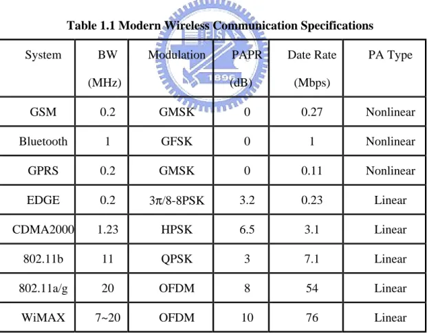
(16) 1.2 Introduction of Transmitter Applications Recently, the demand for higher data rate using the minimum amount of spectrum requires complex modulation technique. Like using Quadrature Amplitude Modulation (QAM) in Orthogonal Frequency Division Multiplex (OFDM) system, makes the using of bandwidth more efficient. Table.1 shows that the higher data rate applications require linear power amplifiers. But linear power amplifier suffers from efficiency problem. EER transmitter is often used to solve the linearity and efficiency trade off.. Table 1.1 Modern Wireless Communication Specifications System. BW. Modulation. PAPR (dB). (MHz). Date Rate. PA Type. (Mbps). GSM. 0.2. GMSK. 0. 0.27. Nonlinear. Bluetooth. 1. GFSK. 0. 1. Nonlinear. GPRS. 0.2. GMSK. 0. 0.11. Nonlinear. EDGE. 0.2. 3π/8-8PSK. 3.2. 0.23. Linear. CDMA2000. 1.23. HPSK. 6.5. 3.1. Linear. 802.11b. 11. QPSK. 3. 7.1. Linear. 802.11a/g. 20. OFDM. 8. 54. Linear. WiMAX. 7~20. OFDM. 10. 76. Linear. 3.
(17) 1.2.1 EER Transmitter. Fig 1.2 Simplified EER transmitter architecture The envelope elimination and restoration transmitter proposed by Kahn [7], [8] as shown in Fig. 1.2. The basic concept is based on splitting the emitted RF input signal into phase-only constant envelope by a limiter. And the envelope information is extracted by the envelope detector. After the extraction of the envelope signal, the amplitude amplifier amplifies the envelope signal to the desired voltage level. Usually, the amplitude amplifier is implemented as the Pulse Width Modulator (PWM) e.g. Class-S modulator. As discussed in 1.3.2, the output voltage of the Class-E power amplifier is proportional to the supply voltage, and efficiency of the Class-E PA under the variable supply voltage remains constant. These two characteristic makes Class-E feasible for recombining the phase and the envelope information with amplification. After all, the combinations of the EER transmitter with the Class-E power amplifier solve the trade between efficiency and the linearity. Hence, a high data rate, high efficiency transmitter could be expected.. 4.
(18) 1.2.2 Applying OFDM in EER When applying OFDM signal in the EER transmitter, the peak to average power ratio (PAPR) of the envelope signal is quite high, that makes the envelope signal highly variable. For example, 802.11a standard applies 64-QAM modulation and 52 OFDM carriers at a data rate of 54 Mb/s.. In this situation (52Mb/s data rate and. 20MHz bandwidth) the PAPR of the envelope signal is 8-10dB. As a result, the modulation accuracy of Class-E power amplifier in the EER transmitter is critical under variable supply voltage. If the Class-E power is suffering from the distortions such as AM/AM and AM/PM distortions (introduced in 1.3.4), the transmitter error vector magnitude (EVM) would be seriously degrade. Nowadays, only the power amplifier proposed in [6] meets the linearity and bandwidth requirements for IEEE WLAN 802.11a data stream 64-QAM OFDM modulation with 20MHz signal bandwidth at 1.6 GHz with 7.2% power added efficiency (PAE) in CMOS process.. 1.3 Class E Power Amplifier. The desire of obtaining high efficiency of the power amplifier is increasing for extending the battery life of the portable device. The power loss of the power amplifiers might come from the non-ideal inductors and capacitors. However, the major power loss in power amplifiers is often result form the power dissipation from the transistors. The power dissipation of the transistors could be released by [3]. A. Minimizing the voltage across the transistor or when current flows through the transistor and the current through the transistor when voltage exists across it.. 5.
(19) B. Minimizing the time intervals when large currents and voltages are applied simultaneously to the transistor. To fulfill requirements A and B, the switch mode Class-E power amplifier is selected.. 1.3.1 Idealized Operations of Class-E PA. The Class-E PA was first published in 1975 [3]. And the idealized operation of the Class-E tuned power amplifier was published in 1977s [4] by Sokal. Fig 1.3 (a) and Fig 1.3 (b) shows the basic circuit and equivalent circuit of the Class-E power amplifier [3].. Fig 1.3 (a) Basic. circuit of the Class-E PA. 6.
(20) Fig 1.3 (b) equivalent circuit of the Class-E PA. The basic Class-E power amplifier includes a voltage controlled MOSFET switch M1 a shunt capacitor, C2, an RF choke, RFC, a series-tuned output circuit, L0C0, and the load resistor, R. C1 is the parasitic capacitance in parallel at the switch including intrinsic transistor output capacitance.. A simple equivalent circuit of the Class-E power amplifier is based on the following five assumptions [4].. ‧The RF choke only allows a dc current and has no series resistance. ‧The quality factor of the series-tuned output circuit is high enough to make the output current is mainly a sinusoid at the operating frequency. ‧The switching action of the active device is instantaneous and lossless. The transistor has zero saturation voltage, zero saturation resistance, and infinite off resistance. ‧The total shunt capacitance is independent of the drain voltage. ‧The transistor can pass negative current and withstand negative voltage. (This is inherent in MOS devices, but requires a combination of bipolar transistors and diodes.) The series reactance jX is produced by the difference in the reactance of the inductor and capacitor of the series-tuned circuit. Note that the jX reactance applies. 7.
(21) only to the fundamental frequency, and it is assumed to be infinite at harmonic frequencies. The nominal component values for the idealized Class-E power amplifier are given by the following equations [4]:. Vdd2 R = 0.577 Pout B(= ωC P ) = 0.183. 1 R. X (= ωL) = 1.152R. (1.1). (1.2). (1.3). If all the circuit components were properly chosen and 50% duty cycle driving input is given, the drain waveform of the ideal Class-E power amplifier acts as Fig 1.4. Fig 1.4 Drain voltage and current waveforms for an ideal Class-E power amplifier.. When the switch is turned off, the current charges the grounded capacitor Cp (parallel capacitor of C1 and C2), making the voltage arise before the switch is turned on (the rise of the voltage is delayed because the presence of Cp). And when the switch is turned on, the capacitor is quickly discharged to the ground and makes the voltage and the slope of the voltage across the switches to zero before the switch is. 8.
(22) turned off again. Therefore, the current and the voltage at the drain were never appeared at the same time, resulting in no power dissipation for transistor. So, an ideal Class-E power amplifier amplification is performed without losses and 100% efficiency. Besides, the output loading network acts as a band pass filter to tune out the non-fundamental harmonic component of the output signal.. 1.3.2 Output power Control for Class-E PA. Fig 1.5 Constant efficiency over supply voltage Instead of providing both the phase and amplitude information at the same time, the Class-E input signal only provides phase only information (ON, OFF information of the MOS switches). Hence the output power is not related to the input signal, which is different from the linear power amplifier. To control the output power, the only way is to vary the supply voltage since it’s the only voltage reference node of the circuit. As a result, every voltage node in the circuit is proportional to the supply voltage and the output power is proportional to the square of the supply voltage. As shown in Fig 1.5 [5] if the only loss is caused from the finite turn on resistance ron. Both the loss and the output power are proportional to the square of the supply voltage (Vdd2).. 9.
(23) Equation (1.4) [5] shows that the efficiency remains constant under variable supply voltage.. Pout , Ploss ∝ Vdd ===> Eff = 2. Pout = const Pout + Ploss. (1.4). Whereas the efficiency of linear power amplifier is only optimized in specified value of supply voltage, Class-E power is more appropriate to apply in the variable supply voltage system and maintain constant high efficiency.. 1.3.3 Limitation of Implementing a Fully Integrated X-Band Class-E PA. The analysis in section 1.3.1 is based on several simple assumptions that are not practical for implementing a fully integrated X-Band Class-E power amplifier. Several reasons that may limit the designing of on-chip X-Band Class-E PA are listed as follow: ‧RF choke implementation Usually, the inductance of the RF choke is quite large. It is not practical to integrate a RF choke in the chip. A large turn spiral inductor will result in significant loss and extremely low resonate frequency below the X-Band. An alternative way is applying the quarter-wavelength microwave transmission line. However, in the X-Band the wavelength is too large to implement for the limited area resource. ‧Nonzero transition time Transistors sizes are often designed to be larger for raising current driving ability.. 10.
(24) However, the larger sizes of transistor offer larger parasitic capacitance. The finite transition time during the charging and discharging could result in tremendous losses and poor efficiency especially at high frequency such as X-Band.. 1.3.4 AM/AM & AM/PM Distortion of Class-E PA. AM/AM distortion and AM/PM distortion are well known as the tow main reasons in Class-E power amplifier that decrease EVM of the EER transmitter under variable supply voltage.. Fig 1.6 AM/AM and AM/PM distortion due to feed through [9]. AM/AM distortion is the nonlinear relationship between the supply voltage and the output voltage. Such a distortion is caused by feeding through from the gate to drain capacitor Cgd that results in non-zero output voltage if no supply voltage is given. This makes nonlinear relationship between supply voltage and output voltage. In low voltage region, the feeding through from gate to drain not only results in AM/AM distortion but also cause AM/PM distortion as shown in Fig 1.6. AM/PM distortion is the unwanted phase shift of the output signal under variable supply voltage. As show. 11.
(25) in Fig 1.6, without the feeding through current, the voltage at the gate will be 180 degree out of phase from the voltage at the drain. If the feed forward current appears at drain, it will shift the output phase. Besides, as shown in Figure 1.6 the shifting is much more seriously in the low supply region. Canceling the feeding through might be a possible solution for eliminating these two distortions at low supply region. A possible approach is to resonate the gate to drain capacitance Cgd by an inductor. However, an extremely large inductor is required, which makes this suggestion not practical. A practical way is applying the pre-distortion function in digital to compensate the distortion when the supply voltage is low. In the high supply voltage, the AM/AM distortion and AM/PM distortion would also happen for the following reasons [10]: 1. Nonlinear drain current versus supply voltage. 2. Nonlinear drain to bulk capacitance variation versus the supply voltage. Figure 1.7 show an example for the AM/AM and AM/PM distortion versus supply voltage Vdd in high and low supply region.. Output voltage. A M /A M. V dd. Output phase. A M /PM. V dd. Fig 1.7 Examples for AM/AM & AM/PM Distortion. 12.
(26) Many works focus on how to decrease the AM/AM & AM/PM distortion by adding a feedback loop in the transmitter. The adding of the feedback loop will result in complex transmitter architecture and instability problem that makes the design of the EER transmitter much more abstruse. Way to avoid feedback is the use of digital pre-distortion. But the pre-distortion must be established based on the given AM/PM characteristic. Solving the distortion in the circuit level analogy way not only simplify the design complication of transmitter design but also makes the integration of single chip transmitter easier. A simple circuit level compensation technique is proposed in this work.. 1.4 Organization. This thesis presents the design of X-Band COMS Class-E power amplifier for EER transmitter. Chapter 2 proposes an X-Band Class E power amplifier for EER transmitter applying injection locking technique to solve the issue mentioned in section 1.3 and helps the reaching of high operating frequency. Also, an AM/PM distortion compensation technique is proposed to release the distortion issue in section 1.3.4 and raising the modulation accuracy of Class-E power amplifier under the high PAPR OFDM envelope signals. Chapter 3 presents the implementation and experimental results of the X-Band Class-E PA including layout descriptions, measurement setup, and measurement results. Chapter 4 establishes an EER transmitter with OFDM IEEE 802.11a data stream. System co-simulation is performed with the proposed circuit. The AM/PM distortion compensation technique will be verified in terms of EVM and spectrum mask. Chapter 5 concludes this thesis and announces the future works.. 13.
(27) Chapter 2 X-Band Class-E Power Amplifier Design for EER Transmitter 2.1 The Proposed Class-E Power Amplifier The proposed fully integrated CMOS Class-E power amplifier applies the injection locking technique and designed in cross couple differential topology centered at the operating frequency of 8.4 GHz. An AM/PM distortion compensation technique is also applied to release the AM/PM distortion in order to meet the linearity and bandwidth specification of IEEE 802.11a. Details of the circuit design and analysis will be shown in the following sections.. Fig 2.1 Proposed Class-E Power Amplifier. 14.
(28) 2.2 Injection Locking Technique for Class-E PA. Injection locking is a general phenomenon that appears in the oscillatory system. For example, a 17th century Dutch scientist Christian Huygens observed that the pendulums of two clocks moved in the very same time if two clocks are tied together. He assumed that the vibrations coupling through the wall drove the other clock into synchronizations. This phenomenon also appears in the oscillator in the circuits, some advantages of the injection locking phenomenon could be used for designing an X-Band Class E power amplifier.. Fig 2.2 (a) Basic LC oscillator (b) Frequency shifting due to additional phase (c) Open-loop characteristics (d) Frequency shift by injection [11]. Figure 2.2 shows a basic concept of the injection locking oscillator. In Fig 2.2a. 15.
(29) the LC tank resonates at the frequency ωo = 1/ L1C1 , the buffer and the transistor M1 produce a 180 degree phase shift separately in the feedback loop. If additional phase is added in the feedback loop as shown in Fig. 2.2b. The total phase shift will be changed by an additional degree φo . In order to maintain the oscillation condition, the tank must provide another phase shift to cancel the phase shift by φo . As shown in Fig. 2.2(c), the oscillating frequency drifts from ωo to a new frequency ω1 . In practical condition, the phase shift φo could be generated by adding a sinusoidal current I inj (with frequency ωinj ) to the drain of the M1. When the injection locking happened, the oscillator frequency will be forced to synchronize to the frequency ωinj . When designing power amplifiers, transistors sizes are often designed to be larger for better driving ability. However, as mentioned in section 1.3.3, it limits the X-Band operation frequency. In order to maintain the current driving ability without increasing the transistors size at X-Band, injection locking technique is applied to solve this problem. Injection locking Class-E power amplifier is based on an oscillator with a positive feedback to input. If no input were given, the circuit acts as a self-oscillating oscillator. However, if the output frequency can be locked with the input frequency, the insatiability could actually increase the driving ability without increasing the transistors size. Usually the series tuned LC Class-E loading network (Lo, Co in fig 1.3) is selected for tuning the waveform to the Class-E waveform for having Class-E characteristics. The well using of oscillator could actually help the power amplifier to reach the high frequency operation with Class-E characteristics.. 16.
(30) 2.3 Differential Cross Couple Topology Injection locking Class-E power amplifier could be implemented either in single ended [12] or in differential topology [5]. In this thesis differential cross couple topology shown in Fig 2.3 (a) is chosen for the reason as following.. vo1. vo2. Fig 2.3 (a) Simplified Cross Couple Differential Topology. vo2. vo1. vo1. vo2 Vin2. Vin1. ron. ron. Fig 2.3 (b) Illustration of the injection locking concepts. 17.
(31) The injection locking is realized in each stage of amplifier parallel with a cross couple pair devices. As shown in fig 2.3 (b), the two input voltage are 180 degree out of phase. The load impedance at the output nodes is properly designed so that the phase of Vin1 and Vo2 is actually the same to control the opposite half circuit. As a result, each of the half circuit is similar to the single ended Class-E power amplifier as shown in Fig 1.1 with the additive advantages as follow:. Ø. The 180 degree phase shift needed for the oscillation is easily generated by the cross couple topology (e.g. in figure 2.3 from Vo2 to Vin1) at any frequencies, which makes the transistors sizing simple.. Ø. The left side of circuit helps the switching of the right side of circuit, so the required transistor size in the input stage can be reduced. After the size reduction of the input transistors, the input capacitances are also reduced. As a result the gain of the amplifier could be increased.. Ø. Instead of discharging the current to the ground or the substrate once per cycle like the single-ended topology, the differential topology discharge twice to the ground per cycle. The undesired substrate noise is thus shifting to the twice time of the signal frequency.. Ø. Although the size of the input transistor is reduced, the turn on resistance ron doesn’t increase due to the parallel topology of the input stage and the cross couple stage.. 18.
(32) 2.4 Circuit Design Considerations. This section describes the circuit design flow of the X-Band Class-E Power Amplifier with CMOS 0.18 µm technology. Section 2.4.1 shows the design of the LC oscillator in the circuit. Section 2.4.2 describes the inductor realization. The output loading network design is shown in Section 2.4.3. Section 2.4.4 shows the simulation results of the X-Band CMOS Class-E Power Amplifier.. 2.4.1 LC Oscillator Design. Vb. Vb. Fig 2.4 LC Oscillator in the circuit. The circuit design begins from the selection of the LC oscillator in the circuit as Fig 2.4. In order to design the circuit at the desired frequency, the oscillating frequency of. 19.
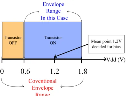
(33) the circuit should be tuned to resonate at the specified frequency. In this work, the LC tank is tuned to resonance at the X-Band transmission band 8.4 GHz. To design the circuit parameter of the LC tank, the DC bias condition is first condidered. To apply the differential cross couple topology in the EER transmitter, the supply voltage (envelope of the emitted signal) range should be varied form 0~1.8V for the 1.8-V CMOS device. However, the gate and the drain of the cross pair M3, M4 are both tied to the supply voltage Vdd as shown in fig 2.5.. Fig 2.5 Bias Condition of transistors M3, M4. The supply voltage Vdd not only serves as the drain voltage of M3, M4 but also as the gate voltage of the M3, M4. As the result, if the supply voltage is under the threshold voltage of the transistor (0.5-0.6V for 0.18µm CMOS technology). The transistor is actually turned off. In the turn off region, the transistor doesn’t act as amplifier and the output voltage is not proportional to the supply voltage Vdd. In this case, the applicable Vdd is only from 0.6V~1.8V. As a consequence, we choose the. 20.
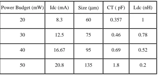
(34) mean value 1.2V of the transistor turn on region (from 0.6 to 1.8V) for the supply voltage (illustrated in Fig 2.6).. Fig 2.6 Illustration of bias decision Next, for the given power dissipation budget, we could calculate the DC current, inductance and capacitance of the LC tank by the following equation:. Pdc = 2Vdd I dc = 2.4 I dc fo =. 1 = 8.4 × 10⁹ 2π Ldc C T. (2.1). (2.2). By applying 0.18µm model and 1.2V supply voltage, a table of the transistor width and the responding value of Idc, CT and Ldc could be derived and summarized in the table 2.1. Usually, the larger dc current can result in larger output power. However, based on the equation mentioned above, the large current needs larger width of transistors and smaller inductance Ldc. For practical layout and routing considerations, this work chooses an inductance value of 0.2nH. If larger output power is desired, designers could scale down the value of Ldc if possible.. 21.
(35) Table 2.1 Transistors width and responding LC value Power Budget (mW). Idc (mA). Size (µm). CT ( pF). Ldc (nH). 20. 8.3. 60. 0.357. 1. 30. 12.5. 75. 0.46. 0.78. 40. 16.67. 95. 0.69. 0.52. 50. 20.8. 135. 1.8. 0.2. After the transistors sizes are decided, all the other parameter in the LC tank are also determined by the following LC tank model and equations.. LT. CT. gT. − g m _ total. Fig 2.7 Half circuit equivalent model of the proposed LC oscillator. ωo =. 1 = 2π × 8.4 ×109 LT CT. (2.3). CT = CNMOS + Cs. (2.4). CNMOS = Cgs 34 + Cdb12 + Cdb 34 + 2(Cgd 12 + Cgd 34). (2.5). 22.
(36) LT = Ldc. (2.6). gT = g o12 + g o 34 + Rs /( Ldcω ) 2. g m _ total = g m34. (2.7) (2.8). where Rs and Cs represent the parasitic of the line inductor Ldc shown in Fig 2.8. Rs. Ldc. Cp Fig 2.8 Line inductor model of Ldc. Once the frequency of input signal enters the locking range (refer to [11]) of the injection locking Class-E power amplifier, the power gain can be immediately boosted. This could tremendously increase the driving ability without large-sized transistors. Overall, the power amplifier output is connected to the oscillator output via a LC tuned pass filter so that the high frequency operation with low harmonics is reached easily without enlarging the transistor size.. 2.4.2 Inductor Realization As mentioned in section 1.3.3 on-chip RF choke for the conventional Class-E power amplifier that makes limitation on designing an X-Band Class-E power amplifier. The section discuss the realization of the DC feed inductor Ldc in the circuit. High Q inductors are required for designing a high efficiency power amplifier. Also,. 23.
(37) the DC feed inductor in the power amplifier carries a large amount of current. So, the target is to design a high Q inductor with excellent current standing ability. From equation (2.1) and (2.2) the value of Ldc is determined to be 0.2nH. The layout of the proposed inductor is shown in Fig 2.9.. Metal 1 Guard Ring. Metal 6. 230 um. Fig 2.9 Layout of the proposed inductor. First the structure of inductor is chosen. Instead of using spiral inductor, the low loss transmission line inductor is applied for having supreme inductor quality factor. Second, the width of the inductor is designed to the maximum width (20µm) of the CMOS 1P6M layout design rule. The maximum metal width could stand about 20mA DC current, preventing the broken of inductor. Third, for having 0.2nH inductance, different length of transmission is simulated with metal 1 guard ring surrounding in EM simulator (the environment of EM simulation will be discussed later). After EM simulation, the inductor length is chosen to 230 µm which producing about 0.2nH at the desired frequency 8.4 GHz. Fig 2.10 shows the EM simulation results of the inductance and the quality factor of the proposed DC feed inductor. The inductor has. 24.
(38) an excellent quality factor over 30 at 8.4GHz.. Fig. 2.10 (a) Inductance versus frequency of proposed inductor. Fig. 2.10 (b) Quality factor versus frequency of proposed inductor versus frequency. 25.
(39) 2.4.3 Class-E Output Loading Network Design. Lo. Co. Lm. Cm. 50 Ohms. Connected to LC tank Matching Network. Fig 2.11 Output Loading Network of the proposed circuit. Usually, the Class-E power amplifier acts as a switch so the current and voltage never appeared at the same time. To achieve this condition the output loading network Lo, Co, Lm, Cm are properly chosen as describe in [7], [13]. For the layout considerations, Cm is absorbed into the output pad. Lo and Lm are combined and the parasitic of the layout components are considered in. The value of output loading network is shown in Fig 2.11.. 2.4.4 Simulation Results of the X-Band Class-E Power Amplifier The proposed circuit is simulated in ADS Fig 2.12 shows the schematic of the proposed X-Band Class-E power amplifier.. 26.
(40) 0.2nH. 0.15 pF. 0.2nH. 1.2nH. 65µ m. 1.2nH. 70 µ m. 65µ m. 0.15 pF. 70 µ m. Fig 2.12 Schematic of the proposed X-Band Class-E PA. PAE (%). Output power (dBm). ‧Output Power & PAE v.s. Supply Voltage. Fig 2.13 Simulation results of output power and PAE v.s. supply voltage @ 8.4GHz. Fig. 2.13 shows simulation results for the output power and power added efficiency (PAE) versus Vdd with 6dBm input power. The PAE from 1.2V to 1.8V shows only 2% variation that verify the Class-E theory in section 1.2.2. This shows that the output power characteristic of the oscillator liked injection locking Class-E power is also suitable for EER transmitter just like conventional ones does. Also, the propose Class-E power amplifier delivers an output power of 9.8dBm and 17% PAE at 1.2V supply voltage.. 27.
(41) However, a critical issue of this circuit appears that might seriously degrade the modulation accuracy of Class-E power amplifier shown in Fig 2.14.. Output phase (degree). Output voltage (V). ‧AM/AM and AM/PM response. Fig 2.14 AM/AM AM/PM response of the proposed Class-E PA The AM/AM response is proportional to the supply voltage. On the other hand, the phase shifting due to AM/PM distortion can be up to 20 degree for the region from 0.6~1.8V supply voltage. In this region, the distortion is due to the variation of the drain to bulk capacitance and nonlinear drain current in function of the supply voltage Vdd that shifts the output phase as mentioned in section 1.5. The strong nonlinearity is a serious damage on the signal transmission and degrading the transmitter EVM. A compensation technique of the AM/PM distortion is proposed in the next section to raise the transmitter EVM.. 28.
(42) 2.5 Proposed Compensation Technique for AM/PM Distortion The AM/PM distortion can be compensated either with digital or analog solution. The use of either one or the other solution depends on the signal frequency and realization technology. Designer choice will affect the complexity and cost of the whole transmitter. In this section, a compensation technique in circuit level analog way is proposed. By applying the proposed technique, the proposed power amplifier could be applied in high envelope PAPR OFDM EER transmitter without increasing the complexity and cost.. 2.5.1 Concept of Distortion From the AM/AM response of the Class-E PA:. Vout = k ⋅Vdd. k <1. (2.9). Equation (2.9) could be an equivalent to Fig 2.15 as a series of two resistance Rload and Rmos, where Rload is the equivalent class-E loading and Rmos is the impedance resulting from the transistor.. Fig 2.15 Equivalence of the AM/AM response. 29.
(43) Zmos can be separated into real and imaginary components Ro (output resistance of the transistors) and B (output capacitance of the transistors). In the realistic case, if Ro and B are functions of supply Vdd that will cause in phase shifting versus Vdd resulting AM/PM distortion (concept as equation 2.10):. ∠(. Vout B(Vdd ) ) = − tan −1 ( ) Vdd Rout + Ro (Vdd ). (2.10). The compensation target is to make Ro and B independent of the supply voltage Vdd to reduce the AM/PM distortion.. 2.5.2 Reasons of Distortion of the Proposed circuit ‧ Nonlinear Drain Current In order to figure out why the shifting of the phase in Fig 2.14 from the region 0.6~1.8V, we bring the design view back to the cross couple topology is reviewed as shown in Fig 2.16.. Fig 2.16 Illustration of the nonlinear drain current of the proposed circuit. 30.
(44) The supply voltage Vdd is tied to the drain and gate of the transistor M3 and M4. As a result, the transistor only enters the saturation region while turning on and the. Idc (A). drain current follows the nonlinear square-law relationship versus Vdd like Fig 2.17.. Vdd (V) Fig 2.17 Drain Current of M3, M4 versus Vdd Since that the output resistance of the transistors Ro is proportional to the inverse of the Idc(Vdd), the nonlinear current plays a important role in the AM/PM distortion. ‧ Nonlinear Output Capacitance of Transistors The output capacitance, drain to bulk capacitance is also a nonlinear function of the drain to bulk average voltage VDB as fig 2.18. Fig 2.18 Nonlinear capacitance of the proposed circuit Besides, CDB follows the equation 2.11:. 31.
(45) C DB =. C j0 V (1 + DB )1/ 2 Vbi. (2.11). Where Vbi is the built-in potential voltage of the body diode and Cj0 is the drain to source capacitance as VDB=0. Fig 2.19 shows the drain to source capacitance CDB at 8.4 GHz versus the supply voltage.. Fig 2.19 CDB variation versus Vdd. When VDB=Vdd changes varies from 0~1.8V the drain to bulk capacitance, producing about 30% variation. Although the cross couple topology solves the limitation of implementation for X-Band operation, when applying in the high PAPR OFDM EER transmitter the nonlinear drain current and the nonlinear variation drain to bulk capacitance versus the supply voltage will result in significant AM/PM distortion. A solution of releasing the distortion will be discussed in the next section.. 32.
(46) 2.5.3 Compensation Technique After figuring out the reason of the AM/PM distortion for the cross couple topology, linerizing the drain current and lower the variation of drain to bulk capacitance CDB will be the design target to compensate the AM/PM distortion while to raise the transmitter EVM. To reach both targets mentioned above, an AM/PM distortion compensation technique is proposed by adding a degeneration linear resistor Rcomp to the source of M3 and M4 as shown in Fig 2.20.. Vdd. Idc. Vdd. M3,M4 Rcomp. Fig 2.20 Proposed AM/PM distortion compensation technique. ‧ Compensation of Nonlinear Drain Current Since Vdd also serves the gate input signal, we know that the conductance of the common source topology follows the equation 2.12.. Gm =. gm 1 + g m RComp. 33. (2.12).
(47) For large gmRcomp, equation 2.12 approaches 1/Rcomp, which is an Vdd. Idc. independent value. Fig 2.21 shows the drain current with and without Rcomp.. Slope of Idc. Fig 2.21 (a) Idc versus Vdd with and without Rcomp. Fig 2.21 (b) Slope of Idc versus Vdd with and without Rcomp The current with the Rcomp is more linear than the current without Rcomp. After linearizing the Idc, the real part of the impedance Zmos in Fig 2.15 could now be an independent value of the supply voltage Vdd.. ‧ Compensation of Nonlinear Output Capacitance Another advantage of applying the degeneration resistance Rcomp is that the variation of the output capacitance CDB could also be suppressed. This is because that the value of VDB is no longer the value of Vdd as shown in fig 2.22. The compensation technique could limit the variation of the VDB so does the CDB. Fig 2.23. 34.
(48) shows the simulation result of the CDB versus Vdd with and without the compensation technique, the variation of CDB with the compensation is smaller and independent of the supply voltage Vdd.. Fig 2.22 Compensation technique for the nonlinear output capacitance. Fig 2.23 CDB versus Vdd with and without compensation technique. As a result, the proposed compensation technique could linearize the drain current and lower the variation of drain to bulk capacitance. The AM/PM distortion will be improved as a consequence; simulation result will be shown in the nest section.. 35.
(49) 2.5.4 Simulation Result with the proposed AM/PM Distortion Compensation Technique. Fig 2.24 (a) Schematic of the proposed circuit. Fig 2.24 (b) AM/PM response with and without compensation technique Fig 2.24 (a) shows the schematic of the circuit and Fig 2.24 (b) shows AM/PM distortion versus the supply voltage with and without the distortion compensation technique. The two curves are almost the same before the transistor is turned on. In this region, the distortion comes from the feed through of the output signal so the compensation topology is not functional in the region. However, as the supply voltage increases, the phase response could be discriminated between tow curves. The curve with the compensation technique is more flat than the curve without the compensation technique. This is because that the nonlinear drain current and the drain capacitance has been linearized. The improvement of the AM/PM distortion could increase the modulation accuracy of the Class-E PA. As a consequence, the transmitter EVM could be improved under the highly variable supply voltage.. 36.
(50) Chapter 3 Implementation and Measurement Results 3.1 Chip Layout Descriptions. The experimental chips are designed and fabricated in UMC 0.18-μm single-poly-six-metal (1P6M) CMOS technology. The implemented circuit is an X-Band Class-E Power amplifier shown in Fig 3.1. The total chip area include pads, as shown in Fig 3.2 , is 900µm×900µm. The target of this experiment is to verify the X-Band Class-E characteristics for the oscillator-like injection locking power amplifier.. 0.2nH. 0.2nH. 0.15 pF 1.2nH. 65µ m. 1.2nH. 70µ m. 65µ m. 0.15 pF. 70µ m. Fig 3.1 Schematic of the experimental circuit. 37.
(51) Fig 3.2 Die photo of the experimental circuit. 3.2 Measurement Results. 3.2.1 Measurement Setup The instruments used in the measurement are listed below:. ‧Signal Generator (ESG). × 1. ‧Power Supply. × 2. ‧Spectrum Analyzer. × 1. ‧Oscilloscope. × 1. ‧ DC Probe (6-pin, 100μm). × 2. ‧ Broadband Balun. × 1. 38.
(52) ‧ Splitter. × 1. The measurement setup is shown in Fig 3.3.. Fig 3.3 (a) Measurement setup for output power and PAE. DC Supply. 6 Pin DC Probe. G. ESG. S. G. G G SS G G. Vin+. BALUN. S. SS G. V in -. Splitter. G. G. 6 Pin DC Probe Oscillosope. DC Supply. Fig 3.3 (b) Measurement setup of AM/PM response. 39. Oscillosope 50 Ohm Terminal.
(53) 3.2.2 Simulation and Measurement Results. ‧DC Measurement First, the DC measurement in Fig 3.4(a) is performed. Fig 3.4(b) shows the measurement and the simulation current versus the supply voltage. Unfortunately, an unpredictable phenomenon happens on the DC current Id.. Fig 3.4(a) DC current measurement. Id (A). Simulation. Measure. Vdd (V). Fig 3.4(b) DC current measurement and simulation results. 40.
(54) Fig 3.4 (c) Data shifting for DC measurement. Measurement results show that there is no DC current if the supply voltage is under 1.1V. By shifting the data of the measurements by 0.6 V in Fig 3.4 (c), we could obverse that the possible reason for the unusual DC current Id might be the process variation of the threshold voltage. However, after shifting the measurement results, the measurement the current is still smaller than the simulation result. The error DC current will result in low power added efficiency and output power. All the bias will be shifted by 0.6V in the following measurements. ‧Test of Injection locking. Fig 3.5 (a) Self oscillation with no input given. 41.
(55) Fig 3.5 (b) Unlock condition with 8.4GHz input signal. Fig 3.5 (c) Injection locking with 8.4GHz input signal. In Fig 3.5 (a), with 1.8-V supply voltage and proper gate bias (0.5-0.7V), the power amplifier shows self oscillation at 8.408 GHz. With the 8.4G input signal is injected, the lower input power level cannot lock the self oscillation as Fig 3.5 (b). As 8.4 GHz the input power level increases, the self oscillation becomes weaker until finally the circuit is forced to oscillate at the input frequency of 8.4 GHz in Fig 3.5 (c). 42.
(56) ‧Output Power & PAE v.s. Input Power @ 8.41 GHz. Pout (dBm) Output power. 10.0. 9.5. 9.0. 8.5 -12.5 -12.0 -11.5 -11.0 -10.5 -10.0. -9.5. -9.0. -8.5. -8.0. Pin (dBm) Input power. Fig 3.6 (a) Output power versus input power @ 8.41GHz. 17. PAEPAE (%). 16 15 14 13 12 -12.5 -12.0 -11.5 -11.0 -10.5 -10.0. -9.5. -9.0. Pin. Fig 3.6 (b) PAE versus input power @ 8.41GHz. 43. -8.5. -8.0.
(57) ‧Pout & PAE v.s. Freq @ 1.8dBm input power 15. Pout Output power (dBm). 10 5 0. Measurement Results. -5 -10 -15 8.34. 8.36. 8.38. 8.40. 8.42. 8.44. 8.46. PAE (%). Output power (dBm). Frequency Freq,(GHz) Hz. Simulation Results. Frequency (GHz). Fig 3.7 (a) Output power versus frequency @ 1.8dBm input power. OutputPAE power (dBm) PAE (%). 20 15 10 5 0 -5 8.34. 8.36. 8.38. 8.40. 8.42. 8.44. Freq, Hz. Fig 3.7 (b) PAE versus frequency @ 1.8dBm input power. 44. 8.46.
(58) ‧Output power & PAE v.s. Vdd. Fig 3.8 (a) Output power versus Vdd. Fig 3.8 (b) PAE versus Vdd. 45.
(59) ‧ AM/AM & AM/PM response ‧. Fig. 3.9 (a) AM/AM response. Fig. 3.9 (b) AM/PM response. 46.
(60) 3.3 Comparison and Summary. Table 3.1 Comparison with the published paper Frequency. Gain. PAE. Pout. Process. Topology. FOM. (GHz). (dB). (%). (dBm). (µm). [14]2006. 17.2. 14.5. 9.3. 17.1. 0.13. NA(linear). 39.7. [15]2005. 18. 16. 23.5. 10.9. 0.13. E. 37.28. [16]2005. 25.7. 8.4. 13.2. 13. 0.13. AB. 12. [17]2003. 17. 11. 2.4. 5. 0.13. NA(linear). 0.276. [18]2006. 5. 24.5. 26.7. 26.5. 0.18. AB. 840. [19]2004. 5.25. 24. 15.3. 19. 0.18. AB. 84. [20]2004. 24. 7. 5. 14.5. 0.18. AB. 4. [21]2004. 5.5. 6. 9. 3. 0.18. A. 0.035. This work. 8.41. 20. 16.25. 9.75. 0.18. E. 10.85. Reference. FOM = Pout × Gain × PAE × f. 2. (W × GHz 2 ). Measurement results show that the proposed X-Band Class-E power amplifier could achieve 17% power added efficiency (PAE) and delivering an output power of 10.75dBm with gain 20dB at 8.41 GHz. Also, the PAE is over 14% over the frequency range 8.35 GHz to 8.45 GHz. The PAE remains constant under variable Vdd and the output magnitude is proportional to the Vdd. This shows that the oscillator-like injection locking power amplifier also exhibits Class-E characteristics. Applying injection locking technique is a feasible way for the X-Band EER Transmitter if the AM/PM distortion is solved.. 47.
(61) Chapter 4 X-Band EER Transmitter Design & Co-Simulation 4.1 Introduction of the Co-Simulation Platform. In order to verify the AM/PM distortion compensation technique, a simulation platform is established in the ADS Ptolemy. Fig 4.1 shows the architecture of the platform. In order to compare with [6], the OFDM broadband 802.11a base band data stream is chosen to verify the function of the AM/PM compensation technique. The transmitter linearity requirements of the 802.11a are listed in table 4.1 [22].. Fig 4.1 EER Transmitter simulation platform. 48.
(62) Fig 4.2 Proposed Class-E PA with compensation topology Table 4.1 Transmitter specifications of 802.11a Number of Carrier. 52. Channel Bandwidth. 20MHz. Data Rate. 6 to 54 Mbps. Carrier Type. OFDM. Modulation. BPSK, QPSK, 16QAM, 64QAM. EVM. 5.6% or -25dB for 54 Mbps. Spectrum Mask. -20 dBc at 11 MHz offset -28 dBc at 20 MHz offset -40 dBc at 30 MHz offset. Envelope Signal PAPR. 8 to 10 dB. The 802.11a baseband modulated signal in Fig 4.1 is up converted by the mixer to 8.4 GHz. After up convertion, a pre-amp is used to increase the input driving power to prevent AM/AM distortion. Following by the pre-amp are the limiter and the envelope detector. These twp circuits split the modulated signal into phase and amplitude component and fed to the proposed Class-E PA in Fig 4.2. All simulation results in the following section are performed with 64-QAM modulation and 20 MHz signal bandwidth which is the strictest system requirement.. 49.
(63) 4.2 Pre-amp Design for AM/AM Distortion. Conventionally, the design target of the pre-amp is to meet the input power level for optimizing the amplifier gain. However, the PA applies the injection locking technique and the output signal is locked by the input signal, the output power doesn’t increase significantly with the input power. The output power of pre-amp should be large to ensure the locking of the output signal. Another view of designing the pre-amp is to optimize the EVM based on the proposed circuit. In order to release the AM/AM distortion, the pre-amp should provide higher input power for Class-E PA. Fig 4.3 shows the AM/AM distortion versus different input power. The AM/AM. Output Magnitude (V). distortion could be released by increasing the input power.. Pin=3dBm. Pin=1dBm. Vdd (V) Fig 4.3 AM/AM distortion versus different input power. After considering the gain and the PAE of the proposed Class-E power amplifier, the output power of the pre-amp is designed to 6dBm. The EVM simulation result could be improved by 3dB with the input power increased from 0dBm to 6dBm.. 50.
(64) 4.3 Gain Design of Amplitude Amplifier After designing the pre-amp, we start to design the gain of the amplitude amplifier. The gain of the amplitude amplifier is commonly considered as related to the supply voltage level of the Class-E PA. However, it also determines the histogram of the supply voltage. The histogram should be chose so that most of the probability of the supply voltage is arranged into the relative linear region of the designed Class-E PA for minimum distortion. Fig. 4.4 (a) shows the histogram of the Class-E supply voltage. The high PAPR OFDM envelope signal results in a widely variable value of supply from 0 to 3.5V which could cause serious AM/PM distortion. By carefully design the gain of the amplitude amplifier, up to 80% of the supply voltage is weighted in the region of .6V~1.8V, which is the relative low distortion region in Fig 4.4 (b). After designing the gain, the EVM improves 2dB to -21dB. An AM/PM compensation technique is required to improve the EVM to -25dB in order to meet the linearity specifications of 802.11a.. Fig 4.4 (a) Histogram of the supply voltage. 51.
(65) Fig 4.4 (b) Relative low distortion of AM/PM response. 4.4 Spectrum & EVM Co-Simulation Results After the designing of the pre-amp and the amplitude amplifier, we start to design the AM/PM compensation topology finally. As mentioned in 2.5.3, increasing the value of Rcomp will result in better linearity. However, the output power and the efficiency are also degraded as the Rcomp increases. A trade off exists between the linearity and the power. The value of Rcomp in Fig 4.2 is designed to 17 Ohms just to meet the linearity specifications with minimum power losses. Fig 4.5 shows OFDM output spectrum and the EVM simulation results with and without the compensation topology. With the compensation, the EVM can be improved by about 4.2dB from -21 to -25.2 dB (-25dB for the spec.) The output power spectrum meets the spectral mask of the IEEE 802.11a signal after the compensation. The 64-QAM OFDM average output power in the 20MHz bandwidth is 9 dBm with an PAE of 15%, driven by 6dBm input power. Table 4.2 summarizes the performance and the comparison of this. 52.
(66) work.. Fig 4.5 OFDM output spectrum and the responding EVM. Table 4.2 Performance Summary and the Comparison of this work This work. ISSCC 2007 [6]. Technology. 0.18µm CMOS. 0.18µm CMOS. Mean Supply Voltage under. 1.1V. 1.7V. Linear 64-QAM OFDM Output Power. 9dBm. 13.6dBm. EVM for 64-QAM OFDM. -25.2dB. -26.8dB. Dissipated Power for PA. 26.4mW. 247mW. Average PAE for 64-QAM OFDM. 15%. 7.2%. Center Frequency. 8.4GHz. 1.56GHz. 64-QAM OFDM. 53.
(67) Chapter 5 Conclusions and Future Works 5.1 Conclusions. An X-Band Class-E power amplifier for EER transmitter is presented in this thesis. The injection locking technique is applied to reach the X-Band operation with gain 20dB,10.25dBm of output power and 17% of PAE. And the AM/PM distortion compensation technique is proposed to raise the EVM by 4.2 dB of the EER transmitter to meet the IEEE 802.11a linearity and bandwidth requirements. This work suggests that CMOS technology is feasible for building a fully integrated high efficiency and high data rate transmitter in X-Band.. 5.2 Future Works The investigation of higher frequency, high efficiency of injection Class-E PA is currently proceeding. Besides, not only for IEEE 802.11a, the proposed circuit might be enhanced to apply in the other modern communication systems with the consideration of the different PAPR and the bandwidth requirements or other system requirements. Another AM/PM compensation technique is needed to solve the trade off between the linearity and the power loss of the compensation topology in this thesis.. 54.
(68) Bibliography [1]. S. Ko, H.D. Lee, D.-W. Kang and S. Hong, “An X-Band CMOS quadrature balanced VCO ,” IEEE MTT-S International Microwave Symposium Digest, vol. 3, pp. 2003-2006 June 2004.. [2]. B. Afshar, A. M. Niknejad “X/Ku Band CMOS LNA Design Technique,” Proceeding of CICC, 2006, pp. 389-392 N. Sokal and A. Sokal, “Class-E A new class of high-efficiency, tuned single-ended switching power amplifiers,” IEEE J. Solid-State Circuits, vol. SC-10, pp. 168-176, June 1975. F. H. Raab, “Idealized operation of the class E tuned power amplifier,” IEEE Trans. Circuits Sys., vol. CAS-24, pp. 725-735, Dec, 1977. K.-C. Tsai and P.R. Gray, “A 1.9-GHz, 1-W CMOS class-E power amplifier for wireless communications,” Journal of Solid-State Circuits, vol.34, no.7, pp. 962-970. Jul. 1999. A. Kavousian, D. K. Su, and B. A. Wooley, “A Digitally Modulated Polar CMOS PA with 20MHz Signal BW,” in IEEE International Solid-State Conference Digest of Technical Papers, February 2007. L. R. Kahn, “Single-Sideband Transmission by Envelope Elimination and Restoration,” Proc. IRE, Vol.40, pp. 803-806, July 1952.. [3]. [4] [5]. [6]. [7]. D. Su and W. Sander, “An IC for Linearizing RF Power Amplifiers Using Envelope Elimination and Restoration,” IEEE JSSC, Vol. 31, pp. 2252-2258, Dec. 1998. [9] P. Reynaert and M. S. J. Steyaert, “A 1.75-GHz polar modulated CMOS RF power amplifier for GSM-EDGE,” IEEE J. Solid-State Circuits, vol. 40, no. 12, pp. 2598–2608, Dec. 2005. [10] A. Diet et al, “EER Architecture Specifications for OFDM Transmitter Using a class E Amplifier” IEEE Microwave and Wireless Components Letters, vol. 14, No. 8 Aug 2004, pp, 389-391. [11] B. Razavi, “A study of injection locking and pulling in oscillators, ”IEEE J. Solid-State Circuits, vol. 39 no. 9, pp. 1415-1424, Sep. 2004 . [12] H.-S. Oh, T. Song, E. Yoon, and C.-K Kim, “A power-efficient injection-locked Class-E power amplifier for wireless sensor network,” IEEE Microw. Wireless Comp. Lett., vol. 16, no. 4, pp. 173-175, Apr.2006. [8]. 55.
(69) [13] K.L.R Mertens and M.S.J. Steyaert, “ A 1.9-GHz, 1-W CMOS Class-E Power Amplifier. Journal Solid State Circuits, vol.37 no.7, pp.962-970. Jul. 1999 [14] V. Andriy“17-GHz 50-60mW Power Amplifier in 0.13-um Standard CMOS, “IEEE Microwave and Wireless Components Letter, VOL. 16 NO. 1 January 2006. [15] C.Cao,H. Hu,Y.Su, and K.K.O, “An 18 GHz, 10.9-dBm Fully Integrated Power Amplifier with 23.5% PAE in 130-nm CMOS,” in Proc. ESSCIRC 2005, Paris, France, Sep. 2005,pp. 137-140 [16] A.Vasylyev, P.Weger, and W,Simburger “Ultra-broadband 20.5-31GHz monolithically-integrated CMOS power amplifiers, “IEE Electron. Lett., vol. 41, no. 23, NOV. 10th, 2005. [17] R. Thuneringer, M.Tiebout, W. Simbuerger, C. Kienmayer and A. L. Scholtz, “A 17 GHz linear 50 ohm output driver in 0.12 um standard CMOS “ in Proc. IEEE Radio Frequency Integrated Circuits (RFIC) Symp., Jun. 2003, pp. 207-210. [18] H. Solar, R,Berenguer, I. Adin, U. Alvardo, and I. Cendoya, ”A fully integrated 26.5dBm CMOS power amplifier for IEEE 802.11a WLAN standard with on-chip “power inductors” in 2006 IEEE MTT-S Int. Microwave Symp. Dig., San Francisco, CA, Jun, 2006,pp. 1875-1878. [19] S. H-L. Tu and S. C. –H Chen, “A 5.25-GHz CMOS Cascode Class –AB Power Amplifier for Wireless Communication, [20] A.Komijani and A. Hajimiri, “A 24GHz +14.5dBm fully integrated power amplifier in 0.18um CMOS, Proc. CICC, pp.561-564, Oct. 2004. [21] Toner B,Dharmalinggam R,Fusco V F.5.5 GHz 802.11a 0.18 μm CMOS pre-power amplifier core with on-chip linearization [J].IEE Proc-Microwave Antennas Propag,2004,151(1):26-30. [22] IEEE, IEEE Standard 802.11-2004, Oct 2004.. 56.
(70) Appendix Measurement Results of a 13.5GHz Class-E Power Amplifier for EER Transmitter A.1 Circuit Descriptions. In order to investigate the higher operating frequency of the EER transmitter, this section shows the measurement results of the experimentation. The implemented circuit is a 13.5GHz Class-E Power amplifier for EER transmitter shown in Fig. A.1. The circuit includes a injection locking Class-E PA operated at 13.5 GHz with the AM/PM distortion compensation topology.. 0.2nH. 0.15 pF. 0.2nH. 0.9nH. 0.9nH. 50µ m. 45µ m. 45µ m. 0.15 pF. 50 µ m. R com p 105µ m. Fig A.1 13.5 GHz Class-E Power Amplifier for EER Transmitter. 57.
(71) Transistor M5 acts as a switch, when Vc is 1.8V the switch is shorted to ground and the AM/PM compensation topology turns off. When Vc equals to 0V the switch opens and the AM/PM topology turns on. The intention of this experimentation is to exceed the X-Band operating frequency and the verification of the AM/PM distortion compensation topology.. A.2 Measurement Results. A.2.1 Measurement Setup. The instruments needed and the setting for the measurement is basically identical to the section 3.2.1 except that a additional supply voltage Vc is fed to the one of the 6 pin DC probe.. A.2.2 Measurement Results. ‧DC Measurement The DC measurement in Fig A.2(a) is performed. Fig A.2(b) shows the measurement current versus the supply voltage. Measurement results of the DC current agree well with the simulation result.. 58.
(72) Fig A.2 (a) Illustration of DC current measurement. 40. IDC. 30. 20. 10. 0 0.0. 0.2. 0.4. 0.6. 0.8. 1.0. 1.2. 1.4. 1.6. 1.8. vdd_measure. . Fig A.2 (b) DC current measurement results ‧Test of Injection locking With 1.8-V supply voltage and proper gate bias (0.5-0.7V), the power amplifier shows self oscillation at 13.49 GHz. With the 13.4 GHz input signal is injected, the lower input power levels for the amplifier cannot lock for self oscillation. As the 13.4 GHz the input power level increases to -2.5 dBm, the circuit is forced to oscillate at the input frequency of 13.4 GHz.. 59.
(73) ‧Output Power & PAE v.s. Input Power @ 13.5 GHz. 20. 12. 15. 10 10 8. PAE PAE (%). Pout (dBm) Output power. 14. 5. 6 4. 0 -4. -3. -2. -1. 0. 1. 2. Pin. Fig A.3 Output power and PAE versus input power @ 13.5 GHz ‧Pout & PAE v.s. Freq @ -0.5 dBm input power. 12. 20. 15. 8 10 6 5. 4 2 13.30. 0 13.35. 13.40. 13.45. 13.50. 13.55. 13.60. 13.65. 13.70. freq1. Fig A.4 Output power & PAE versus frequency @ Pin= -0.5 dBm. 60. PAE (%) PAE. Pout(dBm) Output Power. 10.
(74) ‧Output power & PAE v.s. Vdd (Vc=1.8V). Pout (dBm) Output power. 20. 10. 0. -10. -20 0.0. 0.2. 0.4. 0.6. 0.8. 1.0. 1.2. 1.4. 1.6. 1.8. Vdd (V) Vdd. Fig A.5 (a) Output power versus Vdd when Vc=1.8V. 20. PAE. 10. 0. -10. -20 0.4. 0.6. 0.8. 1.0. 1.2. 1.4. 1.6. Vdd1 Vdd (V). Fig A.5 (b) PAE versus Vdd when Vc=1.8V. 61. 1.8.
(75) ‧Output power & PAE v.s. Vdd (Vc=0V). P (dBm) Output Power. 10 5 0 -5 -10 -15 -20 0.0. 0.2. 0.4. 0.6. 0.8. 1.0. 1.2. 1.4. 1.6. 1.8. vdd1. Fig A.6 (a) Output power versus Vdd when Vc=0V. 20. PAE2 PAE (%). 10. 0. -10. -20 0.4. 0.6. 0.8. 1.0. 1.2. 1.4. vdd2. Fig A.6 (b) PAE versus Vdd when Vc=0V. 62. 1.6. 1.8.
(76) ‧ AM/AM & AM/PM response. sqrt(100*dbmtow(Pout)). 1.4 1.2 1.0 0.8 0.6 0.4 0.2 0.0 0.0. 0.2. 0.4. 0.6. 0.8. 1.0. 1.2. 1.4. 1.6. 1.8. Vdd. Fig. A.7 (a) AM/AM response when Vc=1.8V. sqrt(100*dbmtow(P1)) Output magnitude (V). 0.8. 0.6. 0.4. 0.2. 0.0 0.0. 0.2. 0.4. 0.6. 0.8. 1.0. 1.2. 1.4. vdd1(V) Vdd. Fig. A.7 (b) AM/AM response when Vc=0V. 63. 1.6. 1.8.
(77) 60. phase13 phase12. 40. 20. 0. -20 0.4. 0.6. 0.8. 1.0. 1.2. 1.4. 1.6. 1.8. vdd vadf. Fig. A.8 (c) AM/PM response. A.3 Performance Summary Measurement results show that the proposed Class-E power amplifier could achieve 17.69% power added efficiency (PAE) and delivering an output power of 11.78 dBm with gain 10.28 dB at 13.5 GHz. Also, the PAE is over 13% over the 200 MHz frequency range from 13.4 GHz to 13.6 GHz. The AM/AM and AM/PM response measurement of two conditions are performed. When Vc=1.8V the AM/AM response versus supply voltage shows good linear relationship. When Vc =0V the AM/AM shows different linear response between transistor off and on region. The AM/PM response in this measurement is not much convincing because that as the operation frequency raises to 13.5 GHz, the time domain signal on the scope is very sensitive to noise and swings rapidly so that the phase cannot be measured accurately. Overall, this measurement results show the possibility for investigating the higher operation frequency for EER transmitter. However, another setting for the AM/PM response should be developed to verify the AM/PM distortion compensation topology.. 64.
(78) Vita 姓名 : 王磊中. 性別 : 男. 出生地 : 美國. 生日 : 民國七十三年六月五日. 地址 : 高雄市新興區開封路三百巷二十八號二樓. 學歷 : 國立交通大學電子工程研究所碩士班. 2006/09~2008/06. 國立中興大學電機工程學系. 2002/09~2006/06. 國立高雄師範大學附屬高級中學. 論文題目 :. 1999/09~2002/06. CMOS Class-E Power Amplifier Design for X-Band EER Transmitter 應用於 X 頻帶 EER 發射器之互補金氧半 E 類功率放大器設計. 65.
(79)
數據


+7
![Fig 1.6 AM/AM and AM/PM distortion due to feed through [9]](https://thumb-ap.123doks.com/thumbv2/9libinfo/8464228.183297/24.892.229.662.558.756/fig-pm-distortion-feed.webp)

相關文件
了⼀一個方案,用以尋找滿足 Calabi 方程的空 間,這些空間現在通稱為 Calabi-Yau 空間。.
Robinson Crusoe is an Englishman from the 1) t_______ of York in the seventeenth century, the youngest son of a merchant of German origin. This trip is financially successful,
fostering independent application of reading strategies Strategy 7: Provide opportunities for students to track, reflect on, and share their learning progress (destination). •
Wang, Solving pseudomonotone variational inequalities and pseudocon- vex optimization problems using the projection neural network, IEEE Transactions on Neural Networks 17
volume suppressed mass: (TeV) 2 /M P ∼ 10 −4 eV → mm range can be experimentally tested for any number of extra dimensions - Light U(1) gauge bosons: no derivative couplings. =>
According to the Heisenberg uncertainty principle, if the observed region has size L, an estimate of an individual Fourier mode with wavevector q will be a weighted average of
Define instead the imaginary.. potential, magnetic field, lattice…) Dirac-BdG Hamiltonian:. with small, and matrix
• Formation of massive primordial stars as origin of objects in the early universe. • Supernova explosions might be visible to the most
