Study of Resistive Switching Behavior in ErO
Thin Film for Resistive Random Access
Memory (RRAM)
Study of Resistive Switching Behavior in ErO Thin Film for
Resistive Random Access Memory (RRAM)
Student
Jiun-Ren Chen
Advisor:Prof. S. M. Sze
Prof. Ting-Chang Chang
A Thesis
Submitted to Department of Electronics Engineering and Institute of Electronics
College of Electrical Engineering and Computer Science National Chiao Tung University
in partial Fulfillment of the Requirements for the Degree of
Master in
Electronics Engineering June 2010
/ /
/ /
Study of Resistive Switching Behavior in ErO
Thin Film for Resistive Random Access
Memory (RRAM)
Student
Jiun-Ren Chen Advisor
Prof. S. M. Sze
Prof.
Ting-Chang Chang
Department of Electronics Engineering and Institute of Electronics
National Chiao Tung University
Abstract
Recently, nonvolatile memories have receive greater attention became of their wide application in electronic systems, the conventional floating gate memories are expected to reach certain technical and physical limit in the near future, and the wealth of researches have been proceeded for the next
generation nonvolatile memories.
The resistive random access memories (RRAMs) is a major candidate for the next-generation nonvolatile memory due to its advantages of low power consumption, and high-bit desity, high speed, high endurance and
nondestructive read.
In this thesis, the resistive switching characteristics in Pt/ErOx/TiN device are investigated, and our study can be categorized into seve parts included the
constant voltage stresses, constant current stresses and temperature effect. By exploiting these few kinds of devices and measurement skills, we can investigated the filament formation and redox in the device when resistive switching occurs. We propose a model to explain the phenomenon observed in our experiments.
The model which is electrically driven redox reaction at the local
interface between ErO and TiN electrode behind the filament that is formation in forming process had been established. It can explain the temperature effect and resistive switching behavior under stress. The activate energy had been measured to calculate the retention and read disturb behavior.
FIB
Contents
Abstract (Chinese)………....I Abstract (English)………....II Acknowledgement………..IV Contents……….V Table Lists………..VIII Figure Captions………...IX Chapter 1 Introduction………11-1 Introduction to Non-Volatile Memory………1
1-2 Resistive Random Access Memory………2
1-2.1 Structure and Fabrication……….2
1-2.2 Material Classification………...3
1-2.3 Operation and Circuit Realization……….5
Chapter 2 Experiment………12
2-1 Process Flow………..12
2-2 Material Analysis of Pt / ErOx / TiN Structure……….12
2-2-1 Structure Image of Pt / ErOx / TiN by TEM Analysis………..12
2-2.2 Structure Depth Profile of Pt / ErOx / TiN by AES Analysis………..13
2-3 Electrical Measure of Pt / ErOx / TiN Structure………..13
2-3.1 Resistive Switching Characteristics……….13
2-3.1.1 Current-Voltage Characteristics………13
2-3.1.2 Effect of DC Sweep Condition to The Current-Voltage Characteristics..15
2-3.1.3 Reliability………..…17
Chapter 3 Effect of Geometric Structure………..30
3-1.1 Forming Process………30
3-1.2 Resistive Switching Behavior………31
3-1.3 Summary I………...32
3-2 Cell Size Effect ………..32
3-2.1 Resistive Switching Behavior………32
3-2.2 Summary II………..33
3-3 Modeling………..33
Chapter 4 Research of Resistive Switching Mechanism……….……….41
4-1 Measurement at Different Temperature……….41
4-1.1 Effect of Set Process in Temperature ……….41
4-1.2 Effect of Reset Process in Temperature……….42
4-1.3 SummeryIV………..42
4-2 Sampling……….42
4-2.1 Set Process Sampling………42
4-2.1.1 Constant Voltage Sampling (CVS) in Set Process………..43
4-2.1.2 Constant Current Sampling (CCS) in Set Process………..44
4-2.2 Reset Process Sampling………...44
4-2.2.1 Constant Voltage Sampling (CVS) in Reset Process………..45
4-2.2.2 Constant Current Sampling (CCS) in Reset Process………..46
4-2.3 Activate Energy………...48
4-2.3.1 Activate Energy of Set Process………..48
4-2.3.2 Activate Energy of Reset Process………..…49
Chapter 5 Effect of Thermal Treatment on device……….…63
5-1 Process Flow……….….63
Table Lists
Table 1-1. Comparison of various memories………..7 Table 3-1 The forming voltage in different ErOx thickness……….…35
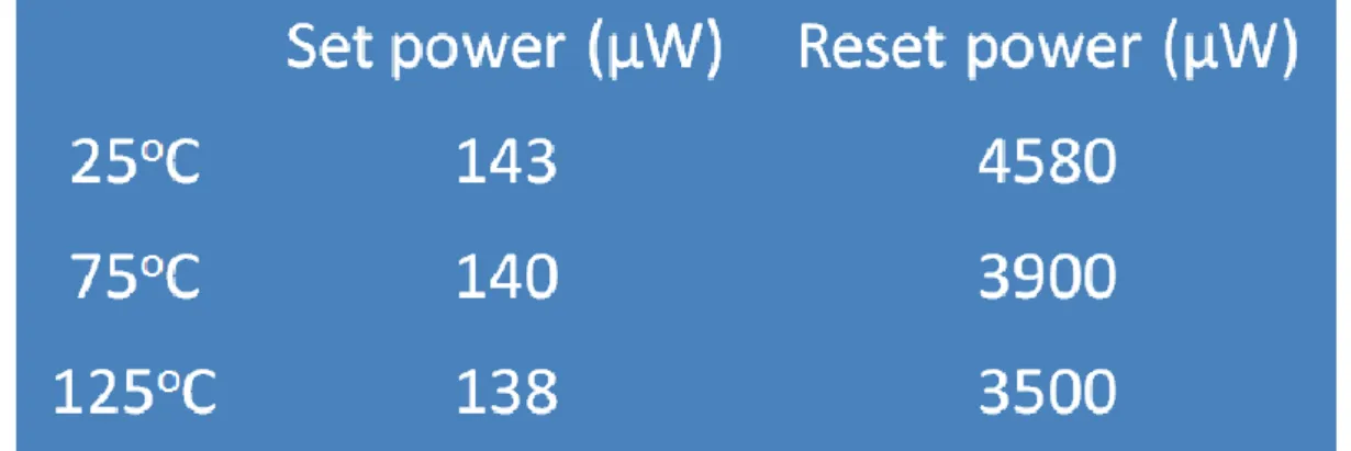
Table 4-1 Compare with set power and reset power in different temperature(25oC,75oC and 125oC) measurement……….…50
Figure Captions
Figure 1-1 Typical I-V curves of RRAM switching in voltage sweeping mode………...7
Figure 1-2 (a) Nonpolar (unipolar) switching (b) Bipolar switching. [98]……….8
Figure 1-3 Switching dynamics monitored with programming and reading pulses. Pulse waveforms and transition for (a) switch on and (b) switch off. [33]………..9
Figure 1-4 Conceptual schematic of 1D1R structure. [40]………9
Figure 1-5 Cross-sectional schematic and basic circuit diagram of 1T1R structure. [24]….…10 Figure 1-6 (a) Generalized cross-point structure with memory and switching elements. (b) Reading interference without switch elements. (c) Rectified reading operation with switch elements.[40]……….10
Figure 1-7 (a) Threshold switching of a Pt/VO2/Pt switch element and (b) Bistable resistance switching demonstrated for a Pt/NiO/Pt memory element. [91]……….11
Figure 1-8 Programming characteristics of combined oxide switch and oxide memory elements.[91]……….11
Figure 2-1 The structure of Pt/ErOx/TiN device………...19
Figure 2-2 The image of cross section for Pt/ErOx/TiN………...19
Figure 2-3 The AES atomic concentration depth profile……….20
Figure 2-4 The negative bias applied on top electrode and bottom electrode ground (set process)………..20
Figure 2-5 The forming process and the forming voltage=-4V………..21
Figure 2-6 The positive bias applied on top electrode and bottom electrode ground (reset process)………..21
Figure 2-7 Typical I-V characteristic of Pt/ErO/TiN device……….22
Figure 2-8 The distribution of resistance of ON and OFF state……….22
Figure 2-10 The I-V characteristic of different current compliances (5,10,15,20mA) in set
process……….23
Figure 2-11 The resistance of ON and OFF state in each current compliance………...24
Figure 2-12 The set voltage in each current compliance………24
Figure 2-13 The reset voltage in each current compliance……….25
Figure 2-14 The I-V characteristic of different stop voltage(1.6,1.8,2V) in reset process……..25
Figure 2-15 The resistance of ON and OFF state in each stop voltage………26
Figure 2-16 The set voltage in each stop voltage………26
Figure 2-17 The reset voltage in each stop voltage……….27
Figure 2-18 2-bit operation (a) Operated by different current compliances (1,5,20mA)(b) Operated by different stop voltage(1,1.4,1.8V)………..27
Figure 2-19 The endurance under DC sweep(100cycles)………..28
Figure 2-20 The endurance under operated by pulse. The Vlow=-1.2V and tlow=1 s for set. The Vhigh=1.5V and thigh=10 s for reset………..28
Figure 2-21 The 104 seconds retention ………29
Figure 3-1 The forming process in different ErOx thickness(3,5,10 and 20nm)………..35
Figure 3-2 The resistance of 100 cycles in ON and OFF state in each ErOx thickness(3,5 and 10nm) device……….36
Figure 3-3 The operating voltage of 100 cycles in ON and OFF state in each ErOx thickness(3,5 and 10nm) device……….36
Figure 3-4 The resistance of 100 cycles in ON and OFF state in each cell size(4μm2,16μm2 and 64μm2) device………37
Figure 3-5 The operating voltage of 100 cycles in ON and OFF state in each cell size(4μm2,16μm2 and 64μm2) device……….37
Figure 3-7 The set voltage-Roff behavior(calculate)……….38
Figure 3-8 The set voltage-Roff behavior (experiment)………39
Figure 3-9 The reset voltage-Ron behavior (experiment)………39
Figure 3-10 The model in initial state(a), ON state(b) and OFF state(c)………40
Figure 4-1 The Vset-Roff behavior in different temperature(25 o C,75oC and 125oC) measurement………50
Figure 4-2 The Pset-Roff behavior in different temperature(25 o C,75oC and 125oC) measurement……….51
Figure 4-3 The Vreset-Roff behavior in different temperature(25 o C,75oC and 125oC) measurement……….51
Figure 4-4 The Preset-Roff behavior in different temperature(25 o C,75oC and 125oC) measurement……….52
Figure 4-5 Top electrode give a constant voltage stress (CVS) or constant current stress (CCS) and bottom electrode grounding……….52
Figure 4-6 The current transition in different stress voltage(0.68,0.67,0.66,0.65 and 0.64V) in set process……….53
Figure 4-7 The transition time relate to stress voltage………53
Figure 4-8 The voltage transition in different CCS(0.6,0.55,0.5 and 0.45mA) in set process..54
Figure 4-9 The transition time relate to different CCS(0.6,0.55,0.5 and 0.45mA) in set Process………..54
Figure 4-10 In Situ observation of current overshoot in set process[94]……….55
Figure 4-11 The temperature(e) current (c) and voltage (a) on the device in set process[95].56 Figure 4-12 The current transition with time under different CVS in reset process……….56
Figure 4-13 The transition time relate to different CVS in reset process……….…….57 Figure 4-14 The current transition with time under different CVS(0.85,0.9,0.95 and 1V) which
Figure 4-15 The voltage transition with time under different CCS in reset process………58 Figure 4-16 The transition time relate to different CCS in reset process……….58 Figure 4-17 The voltage transition with time under different CCS with voltage compliances in
reset process……….……..59 Figure 4-18 The final resistance after different CCS with voltage compliances in reset
Process……….………...59 Figure 4-19 (a)Keep power on the device after CCS with voltage compliances in reset
process, and(b)final resistance([email protected])...60 Figure 4-20 The reset process, oxygen ion recombine with oxygen vacancy…….………60 Figure 4-21 The transition time relate to different CVS(0.47,0.5 and 0.53V) in different
temperature(275,250 and 225K) in set process………61 Figure 4-22 The activate energy in 0.47V is 0.392eV(a), Vs=0.5V is 0.24eV(b), 0.53V is
0.19eV(c). And extrapolate to 0V the activate energy is 1.4eV………61 Figure 4-23 The transition time relate to different CCS in different temperature in reset
process……….62 Figure 4-24 The activate energy in 7.5mA is 0.149eV(a), 8mA is 0.098eV(b), 8.5mA is
0.0466eV(c). And V=IR,R=100Ω then extrapolate to 0V the activate energy is
0.92eV………..62 Figure 5-1 The 1T1R structure………65 Figure 5-2 The forming process in each device(non-annealing, 400,500 and 600oC
annealing)………..65 Figure 5-3 The 600oC device without resistive switching characteristic……….….66 Figure 5-4 The ON state resistance in non-annealing, 400 and 500oC annealing device.……66 Figure 5-5 The OFF state resistance in non-annealing, 400 and 500oC annealing device.…..67 Figure 5-6 The set voltage in non-annealing, 400 and 500oC annealing device………….……67
Chapter 1
Introduction
1-1 Introduction to Non-volatile Memory
Memories can be divided into two main categories: volatile and nonvolatile. Volatile memories lose their data as soon as the system turned off. Most
random access memories (RAM) fall into this category. Nonvolatile memories do not lose its data when the system or device turned off. Examples of
non-volatile memories include read-only memory, flash memory, most types of magnetic computer storage devices (e.g. hard disks, floppy disks, and
magnetic tapes), optical discs, and early computer storage methods such as paper tape and punch cards a long time. The first semiconductor NVM is the floating-gate nonvolatile memory, invented by S. M. Sze and D. Kahng in 1967. NVMs have been widely used in the portable devices recently, such as flash memory devices, cell phones, digital cameras, mp3 players, and personal digital assistants. A perfect NVM should have the properties including low operating voltage, simple structure, low power consumption, non-destructive readout, high operating speed, long retention time, high endurance, and small cell size. There are been many sorts of nonvolatile memories proposed so far in addition to the floating gate memories, such as phase-change memory (PCRAM), ferroelectric random access memory (FeRAM), magnetoresistive random access memory (MRAM), and resistance random access memory (RRAM). Nowadays, flash memory is the mainstream among the NVMs.
1-2 Resistive Random Access Memory
RRAMs are good for the resistance changes for different memory states. By electrical field or current effects, the conductivity of the memory layer can be switched between high and low resistance reproducibly. The different resistance states stands for different digital states as memory devices. The strengths of RRAM are high cell density array, high operating speed, low power consumption, high endurance and lower scale limit. Furthermore, RRAMs have the features of nonvolatility , long retention time, and
non-destructive readout. In this section, the properties are discussed in view of the structure, fabrication, material classification, operation and circuit
realization. Table 1.1, RRAMs have great potential to replace the flash memory and will become mainstream memory in the future.
1-2.1 Structure and Fabrication
The basic structure for RRAM is made up of only metal-insulator-metal, MIM, which can be further integrated into 1D1R (a diode and a resistor), 1T1R (a transistor and a resistor) structures (discussed later), or 1S1R (a switching and a resistor). The top and bottom electrodes could be metals or conducting transition metal oxides, the choice of which has impacts on the resistive
switching properties because of their different crystallinities, work functions and the ability of Gibbs free energy. The adhesion and among layers should be considered as well. If high temperature process is needed, the thermal stress problem should be considered. The main character of resistive switching is the insulator layer sandwiched between the electrodes. The insulator for the MIM structures actually may be not really insulating, but also semiconducting,
depending on the constitution and stoichiometry. Usual deposition methods of the insulator are many and various, including radio-frequency (RF) magnetron sputtering, reactive sputtering, e-beam evaporation, spin coating (sol-gel), thermal oxidation, metal-organic chemical vapor deposition (MOCVD), pulsed laser deposition (PLD), atomic layer deposition (ALD), plasma-enhanced atomic layer deposition (PEALD), and melt-grown by FZ method. Among them, the sputtering has lower cost and wide application but poor film uniformity; e-beam evaporation and spin coating has low process cost but poor film quality as well; thermal oxidation are suitable for high reactive metal like Ni, Ti or Cu to form metal oxides and inexpensive; MOCVD, PLD, ALD, and PEALD are able to produce high quality film with good step coverage but expensive; the FZ method is able to fabricate perfect crystals with exact component proportion but not practical in semiconductor fabrication process. The different quality deposited by different methods has connection with the resistive
switching characteristics.
1-2.2 Material Classification
The resistive switching phenomena have been found in many materials. The research mainstream is focused on several groups, including binary oxides, perovskite oxides, manganites, and other alloy or polymers.
The binary oxides adopted in RRAM application, such as CuxO [1-16], TiO2 [17-32], NiO [33-53], ZrO2 [54-65] Al2O3 [66-68], HfO2 [69,70,73,93], Fe2O3 [71], ZnO [72] and MoOx [74], are candidates or have been widely used in other field of CMOS devices. Thus the compatibility with modern CMOS process would not be a problem. Moreover, this material group of
binary oxides has simpler element components. It is easier to control the proportion of metal and oxygen elements. Another extensively studied material group is (Ba,Sr)(Zr,Ti)O3, BSZT. It has been studied as a role of the high-k dielectric for a long time [75]. Many BSZT in RRAM are doped with V [76], Cr [77,78], etc. Dopants are prone to occupy sites of intrinsic oxygen vacancies, and thus restrain the formation of them [76]. Because of the more components and the more complicated chemical environment, the control of the component proportion is not as easy as that of binary oxides.
The manganites discussed in RRAM usually represent the carrier-doped manganites with perovskite structure, R1-xAxMnO3, where R and A are
rare-earth and alkaline-earth ions, respectively [79-84]. They are not classified in the above perovskite system here because of their unique characteristics of conducting ferromagnets below a Curie temperature [79]. Manganites with perovskite structures exhibit a magnetoresistive response that is many orders of magnitude larger than that found for other materials, beside the electrical resistive switching behaviors. It is the epitaxial samples that are generally prepared by PLD [81,83] or floating-zone melt-growth method [79] to obtain the precise element proportion and physical properties. For the same reason of perovskite oxides, the future for manganites in RRAM is not so promising.
The other materials such as chalcogenide (GeSbTe) [85], sulfides (e.g. Cd1-xZnxS [86]), and organic materials including Rose Bengal sodium salt (RB) [87], copperphthalocyanine (CuPc) [88], 2-amino-4,5-imidazole dicarbonitrile (AIDCN) [88] and so on, have been investigated for RRAM application. The chalcogenidematerial has been drawing many attentions recently due to Intel’s support, while the others are newly introduced to
semiconductor processes. Besides, many organic polymers tend to degrade easily. Chalcogenide seems a more practical candidate in this group of
materials.
1-2.3 Operation and Circuit Realization
Basic operation of bistable resistive switching in a single cell can be achieved by DC sweep or pulse switching methods. Figure 1-1 shows
a typical I-V plot under DC sweep operation. Assuming the resistance state is first held in OFF state (high resistance state), the current suddenly increases as the DC bias sweeps toward positive direction and ON state (low resistance state) is reached, which is defined as a process of “set” as indicated in the figure. The voltage where the current suddenly increase is the set voltage. Then a negative voltage bias is applied to switch back to OFF state with a substantially current drop at the reset voltage, as indicated by the “reset” in the figure. It should be noted that this operation requiring different voltage
polarities to switch ON and OFF, whether positive on/negative off or positive off/negative on, is called bipolar operation. As for the unipolar operation, either polarity can be applied to switch on or off depending on the present memory state. On the basis of I–V characteristics, the switching behaviors can be classified into two types: unipolar (nonpolar) and bipolar, for which typical I–V curves as shown in Figure 1-2a and 1-2b, respectively. For the data reading operation, the bias should not exceed the range indicated as “read” in the figure to prevent memory state modification. Figure 1-1 does not show the forming process required to initiate the resistive switching properties of as-deposited oxide films. The forming process is similar to soft oxide
breakdown, leading to the conducting paths (filaments) composed of clusters of point defects. To unify and clarify the terms of operating parameters in the following text, the “set” and “reset” would be used to describe the switching operation ; “Vset”, “Vreset”, “Ron” and “Roff” instead of “set voltage”, “reset voltage”, “on-state resistance” and “off-state resistance”.
In the real circuits, it is the pulse switching that is the practical
operation method for its fast operation speed and lower power consumption. The waveforms of switching on and off are shown in Figure 1-3(a) and (b) respectively. The pulse heights and widths for switch on and off must strike a balance, in which the larger the pulse heights are, the shorter the pulse widths are needed. The reading pulses with small pulse heights are designed not to modify the memory states.
For the memory cell array, 1D1R, 1S1R, 1T1R structure as shown in figure 1-4 to figure 1-8 must be used to prevent misreading as shown in figure 1-6. I. G. Baek et al. [33] reported that if a cell is in off state and its neighboring cells are in on state, it will be misread as on state because of the leakage current path around its neighboring cells. Therefore, a rectifying element is required for each cell in an array to confine the current paths. The minimum sizes for 1D1R and 1T1R structures are 4F2 and 6F2 respectively, which meet the requirement for high density arrays.
Table 1-1 Comparison of various memories
Figure 1-3 Switching dynamics monitored with programming and
reading pulses. Pulse waveforms and transition for (a) switch on and (b) switch off[33]
Figure 1-5 Cross-sectional plot and basic circuit diagram of 1T1R structure[24]
Figure 1-6 (a) Generalized cross-point structure with memory and switching elements. (b) Reading interference without switch elements. (c) Rectified
Figure 1-7 (a) Threshold switching of a Pt/VO2/Pt switch element and (b) Bistable resistive switching demonstrated for a Pt/NiO/Pt memory element [91]
Figure 1-8 Programming characteristics of combined oxide switch and oxide memory elements[91]
Chapter 2
Experiment
2-1 Process Flow
The Pt / ErOx / TiN cell were fabricated by following processes. A buffer oxide grown on p+-Si substrate by thermal oxidation. After
growing the buffer oxide, the bottom electrode (BE) TiN and adhesion layer Ti were deposited. Subsequently low temperature oxide (LTO) deposited on TiN/Ti/SiO2/p+-Si substrates and patterned via holes and BE contact pads were defined by lithography and etch .After that, a second lithography defines the via and the top electrode contact pad, Then, a 10-nm-thick ErOx deposited on the via hole by reactive sputtering using Er target in O2 ambient (Ar:O2=24:5) at room temperature. After growing ErOx ,70-nm-thick top electrode Pt
deposited by dc sputtering at room temperature. Finally lift off. The cell size defined by the via hole was 0.01μm2 to 64μm2
. Figure 2-1 shows the structure.
2-2 Material Analysis of Pt / ErO
x/
TiN Structure
2-2.1 Structure Image of Pt / ErO
x/ TiN by TEM Analysis
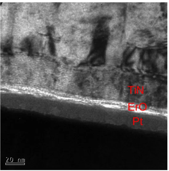
Figure 2-2 shows the image of cross section for Pt / ErOx (10nm)/ TiN structure . The thickness of ErOx is about 10nm that can be, It matches what we predict.
2-2.2 Structure Depth Profile of Pt / ErO
x/ TiN by AES Analysis
Atomic concentration depth profile of Pt / ErOx / TiN structure analyses by auger electron spectroscopy (AES). The result are shown in figure 2-3 .
Detected elements in the structure are Platinum (Pt), Erbium (Er), Oxygen (O) and Titanium (Ti). Titanium (Ti) and Nitrogen (N) have the same energy peak, so Titanium was detected only. After thirty minutes sputtering, the signal of Oxygen (cycle) is correspond with the signal of Erbium (triangle up). The atomic concentration ratio of Erbium and Oxygen is 1:1. The ErOx film is Erbium rich cause Er2O3 is stoichiometry. Therefore, There are many oxygen vacancies in the ErOx thin film.
The Ti is strong oxygen gettering, so the interface between ErO and TiN are mixed of Er, Oxygen and Ti.
2-3 Electrical Measure
The electrical properties were measured by the apparatures consisting of a probe station with temperature controller, Keithley4200 semiconductor characterization analyzer and low leakage switch, control by a Keithley 4200 computer.
The method of measurement were bias on the top electrode Pt and bottom electrode TiN grounded.
2-3.1 Resistive Switching Characteristics
2-3.1.1 Current-Voltage Characteristicsprocesses high resistance value before forming process, as shown in figure 2-5 . Top Pt electrode is applied a large negative voltage which will produce a high electric field on ErOx layer. Hence, the breakdown of impact ionization would happen in ErOx. Figure 2-5 shows the I-V curve, a DC sweep applied on top Pt electrode from 0V to -5V with voltage step is -0.2V,and bottom electrode TiN is grounding, as shown in figure 2-4 , ErOx film breakdown when -4V (forming voltage). In order to avoid the device being permanent damage, the measurement parameter would set a current compliance (Ic) which is
controlled by a feedback system in apparatus. After forming process, the resistance value become lower, it is low resistance state (LRS) or ON state. There is(are) conducting filament(s) (CF)in the ErOx layer, The CF is
composed by oxygen vacancies.
Device is ON state after forming process, reset process is the second step to switch resistance value to higher. The Pt top electrode applies positive voltage, and the bottom electrode is grounding, as shown in figure 2-6.
Positive voltage side in figure 2-7 shows the I-V curve of reset process, the DC sweep is 0V to 1.5V with voltage step 0.05V, when 1V (reset voltage). Then the current decreases with voltage increases, it shows a negative resistance, it means that resistance value of device become larger . After the reset process, the resistance value shows larger than ON state , names high resistance state (HRS) or OFF state.
The set process is the following step to switch resistance after reset process. The voltage sweep from 0V to -2V with voltage step -0.05V, as shown in figure 2-7, when voltage equal to -0.6V (set voltage), the device breakdown again , but the breakdown voltage is smaller than forming process, The same
to forming process, in order to avoid the device being permanent damage, the measurement parameter would set a current compliance (Ic) which is
controlled by a feedback system in apparatus
Figure 2-7 shows two different resistance value between ON and OFF state, that is define Ron and Roff , Ron and Roff is the voltage over current at 0.2V (read voltage). The ratio of Ron and Roff is 10 to 1000 times. The Ron, Roff and ON/OFF ratio depends on the DC sweep condition. It is important that the device for in multibit memory applications.
Figure 2-8 and figure 2-9 are extracted the distribution which were operated 100 cycles. Figure 2-8 shows the distribution of Ron and Roff , the distribution is acceptable. It didn’t overlap that can be read the state without fault. Figure 2-9 shows the distribution of Vset and Vreset , it is stable which could be operated without switching fail. The device shows feasible application for memories
2-3.1.2 Effect of DC Sweep Condition to The Current-Voltage Characteristics
In this section, the I-V characteristics on different operator condition will be discussed.
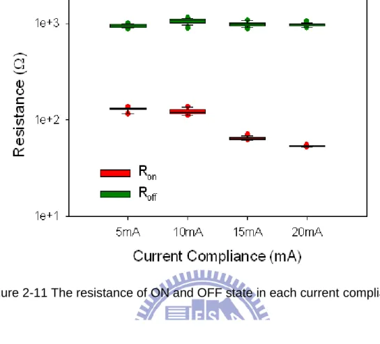
The resistance value of ON and OFF state depend on the DC sweep condition. In figure 2-7, the Ron and Roff are controlled by the current compliance in set process and the voltage sweep to stop voltage (Vstop) in reset process. The higher current compliances induce lower Ron, and larger Roff is due to larger Vstop.
Figure 2-10 shows the current-voltage curve with different current compliances (5mA, 10mA, 15mA and 20mA) in set process. The device
operated 100 times each current compliance, then read the distribution (100 cycles) of Ron and Roff at 0.2V, in 100 cycles, the results show in figure 2-11.It shows the Ron depends on the current compliance and Roff doesn’t . It is clear that the current compliance varies in set process, so it control the Ron but not Roff. The higher current compliances makes smaller Ron, the device get many resistance value with different current compliance. But it has reliability and power issue under large current compliance.
In this paragraph, the operating voltage is discussed with different DC sweep conditions. Figure 2-12 shows the set voltage (Vset) with different current compliance in 100 times cycle, the Vset is modulus, actually Vset is negative. And reset voltage (Vreset) with different current compliances, as shown in figure 2-13. The two figures show the reset voltage depends on the current compliance, but set voltage dosent. The set voltage increases with higher current compliances.
Previous two paragraphs imply that the reset voltage maybe depend on the Ron not current compliance, and set voltage depends on the Roff , therefore, the set voltage show constant with different current compliances.
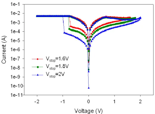
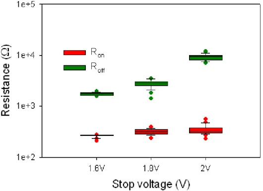
Now it is discussed the effect of stop voltage. Figure 2-14 shows the current-voltage curve with three different stop voltages 1.6V, 1.8V and 2V. The resistance value of ON and OFF state of 100 times cycle as shown in figure 2-15. It is obvious that different reset process condition only control the following OFF state, the larger stop voltage induce higher resistance value of OFF state.
The same to previous paragraphs, it should discuss the effect of operating voltage. Figure 2-16 and figure 2-17 show the set voltage and reset voltage
under different reset process condition. It shows different stop voltage make set voltage shift and reset voltage dosen’t. This result implies the set voltage shift is due to the Roff shift.
Now we know that the operating voltage depends on the resistance value, and resistance value can be controlled by the DC sweep condition we apply. There are two ways to apply on multilevel memories, one of them is current compliances, the other is stop voltages.
Figure 2-18 shows the 2-bit operation by DC sweep in 100 times. Figure 2-18(a) was operated by different current compliances in set process, figure 2-18(b) was operated by different stop voltage in reset process. Both two ways show workable.
2-3.1.3 Reliability
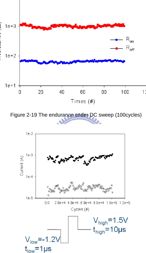
Endurance is a key feature about memory device. After enormous number of switching cycles, the memory device must meet the operation requirement in many applications, such as access memory (RAM) and solid state disk (SSD). Because these applications need many data write-in operation without any failures, endurance is a basic requirement in almost every type of memory device. The tests of endurance were carried out by DC bias and pulse. Figure 2-19 is the endurance which were operated 100 times using DC sweep, it shows stable and without degradation. Figure 2-20 is the device switch under pulse operation. The Vlow=-1.2V and tlow=1 s for set. The Vhigh=1.5V and thigh=10 s for reset. It shows good endurance under 105 time operations.
stands for the capability of retaining memory data for a long period without any data loss. For a commercially available nonvolatile memory product, the
performance of retention is requested to keep ten years. The retention tests were carried out by DC biases which would switch devices to ON or OFF state. Then, The data states were read out once in a given period by applying a small voltage in order not to disturb the memory state which is 0.2V reading bias. Figure 2-21 shows the 104 second retention. The Ron shows good retention. That could be read the state without fault. The Roff shows resistance value shift, but it become higher resistance value, that is not effect to read the state. But it would effect the multilevel operation on the OFF state.
Figure 2-1 The structure of Pt/ErOx/TiN device
ErO
TiN
Pt
Figure 2-3 The AES atomic concentration depth profile
Figure 2-4 The negative bias applied on top electrode with bottom electrode grounded (set process)
Figure 2-5 The forming process and the forming voltage=-4V
Figure 2-9 The distribution of set and reset voltage
Figure 2-11 The resistance of ON and OFF state in each current compliance
Figure 2-13 The reset voltage in each current compliance
Figure 2-14 The I-V characteristic of different stop voltage(1.6,1.8,2V) in reset process
Figure 2-15 The resistance of ON and OFF state in each stop voltage
Figure 2-17 The reset voltage in each stop voltage
Figure 2-18 2-bit operation (a) Operated by different current compliances (1,5 and 20mA)(b) Operated by different stop voltage(1,1.4,1.8V)
Figure 2-19 The endurance under DC sweep (100cycles)
Figure 2-20 The endurance under operated by pulse. The Vlow=-1.2V and tlow=1 s for set. The Vhigh=1.5V and thigh=10 s for reset
Chapter 3
Effect of Geometric Structure
In order to know the device characteristics when the device scaling down. In this chapter, the thickness of ErO and the cell size would be discussed.
3-1 Thickness Effect
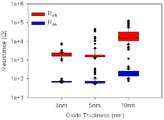
Pt / ErOx / TiN structure were fabricated, and thickness of ErOx are 3nm, 5nm, 10nm and 20nm. The 20nm-thickness ErOx devices show bad stability resistive switching, so it would not discuss detail here.
3-1.1 Forming Process
Table 3-1 show the forming voltage of different ErOx thickness and Figure 3-1 show the I-V in forming process. The thicker ErO shows higher initial resistance and larger forming voltage. The forming voltage strongly depends on the oxide thickness. The thicker oxide need larger voltage to gain enough electric field, that electron could get energy and impact the oxide to disrupt the banding between Er and O.
It is known that the Ti is strong oxygen-gettering, at the interface between ErOx and TiN, the ErOx would become Er metal due to the Ti getter the oxygen. The interface shows metal-like which has smaller resistance than bulk ErO. After observe the Table 3-1, we can predict that the resistive switching layer is between 5nm to 10nm. Because the forming voltage in 5nm-device
equal to set voltage. That means the device dose not need breakdown the bulk ErO. Therefore, the resistive switching layer would be thicker than 5nm. The 10nm-device show forming voltage (-5V) larger than set voltage (-1V). It need breakdown the bulk ErO in forming process. Therefore, the resistive switching layer would thiner than 10nm.
3-1.2 Resistive Switching Behavior
In 2-3.1.1, it is found that the set voltage is always smaller than the forming voltage but the 3(5) nm-thickness device not. Both set and forming process are oxide soft breakdown, it implies the breakdown of oxide’s thickness is different in two process, and the initial resistance is larger than Roff .
After forming process, the oxide is almost breakdown and damage which can’t recover, only less region can recover which is not damage completely, Therefore, the region can recover is the resistive switching area which can be operated cycle by cycle. In obvious literature, it shows the resistive switching region is at the interface between oxide and TiN electrode and the region is total layer at the interface. Because the interface show small resistance, when breakdown happened, the current flow through this area, the damage is
smaller.
Figure 3-2 shows the Ron and Roff in each devices (3nm,5nm and 10nm). The 10nm-device show larger resistance both ON and OFF state. It shows the resistive switching layer is thicker.
Figure 3-3 shows the set and reset voltage in each device. It shows similar operating voltage in each device.
3-1.3 Summary I
The aim of RRAM device is formingless and stable switching. We could find the resistive switching layer thickness and fabricate suitable device to reach the aim.
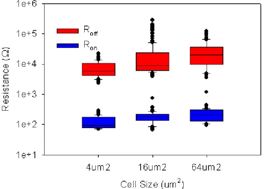
3-2 Cell Size Effect
Pt / ErOx / TiN structure were fabricated. The cell size is 0.01μm2 to 64μm2 . Because the smaller via holes have bad step coverage, the cell size about 1μm2
device shows bad yield. It wound be not discussed here. Here, we discuss three different cell size devices (4μm2,16μm2 and 64μm2
)
3-2.1
Resistive Switching Behavior
Figure 3-4 shows the Ron and Roff in 100 times operation in three cell size device(4μm2,16μm2 and 64μm2
). It shows similar in each device. And figure 3-5 shows the operating voltage in each device. There are no different between them.
It would be know the Ron dose not depend on the cell size, but Roff dose. But figure 3-4 shows not. It maybe the variation between devices or some else reasons.
We find a method to analysis the device cell size-depend or not. Figure 3-6[93] is the model well know and the public accept. The filament was formed in forming process. And the resistive switching layer at the interface between ErO and TiN. Therefore the Roff would be size-depend. Now we know the set process is oxide breakdown, and the breakdown voltage depend on the
resistive switching thickness in OFF state. The Vset-Roff would be like figure 3-7, the linear relationship between Vset and Roff, the higher Roff make higher Vset cause
L A R
The larger L make higher resistance and breakdown voltage. If there are two devices have same resistive switching layer thickness L and different cell size A, like 4μm2 and 64μm2
, the result would be figure 3-7.
Figure 3-8 is the experiment data, it dose not split between different cell size device, it shows the Roff isn’t size-depend. Figure 3-9 shows the Vreset-Ron , for the same reason the ON state is size-independent, too.
3-2.2
Summary II
In the research of cell size effect, we found that the resistive switching layer is independent of the cell size both ON and OFF state. This is different from the reference which always indicate the OFF state is size-dependent and ON state size-independent.
For this reason, we will establish our model for our devices.
3-3 Modeling
Figure 3-10 shows the model in initial state (a), ON state (b) and OFF state (c). The open circles are oxygen vacancies and close circle are oxygen. Figure 3-10(a) shows the initial state before forming. It is known that the ErOx thin film which is Er rich in AES depth profile analysis, so there are many oxygen vacancies in the ErOx thin film. The oxygen at the interface between ErOx and TiN would be gettering, so the oxygen vacancies at the interface are more and more than initial ErOx film. If the devices are applied a enough voltage that can establish a critical electric field. Electrons got energy from the electric field than impact the Er and O banding and disrupt the banding. After the banding disrupted, the current become larger than the more energy input,
the electron got larger energy to disrupt the band. This is a positive feedback to breakdown. We would set a current compliance to disrupt the positive feedback. In the forming process, the interface is initial lower resistance, it is not damage completely in the positive feedback and could be recover. But the interface layer beyond the path of the filament, which is more damage than the other interface layer. After the forming process, the interface layer shows localize low resistance as shown in Figure 3-10(b). There are more oxygen vacancies beyond the filament than the others areas.
Figure 3-10(b) shows the ON state, the ON current flow though the filament and the interface layer at localized area, There are higher oxygen vacancy density, the higher oxygen vacancy density mean lower resistance. According to Ohm law, it is clear to know the current is flow through local area. Therefore, the ON current shows cell size-independent.
Following we should reset the device, If we apply a positive voltage on top electrode, a electric field is establish from bottom electrode to top electrode, and a large current flow through cause low resistance, which make
temperature increase. Under heating and electric field, the oxygen which is getteringed by the TiN electrode become release, and move to ErOx layer the oxygen ion recombine with the oxygen vacancies. The oxygen vacancy density decrease means the resistance increase, the device become OFF state as shown in figure 3-10(c).
At 3-2.1 the OFF current is independent of cell size, it implied the oxygen vacancy density is higher than the other area which damage level is lower, even the resistive switching layer is OFF state, as shown in figure 3-10(c)
Table 3-1 The forming voltage in different ErOx thickness
Figure 3-2 The resistance of 100 cycles in ON and OFF state in each ErOx thickness(3,5 and 10nm) device
Figure 3-3 The operating voltage of 100 cycles in ON and OFF state in each ErOx thickness(3,5 and 10nm) device
Figure 3-4 The resistance of 100 cycles in ON and OFF state in each cell size(4μm2,16μm2 and 64μm2
) device
Figure 3-5 The operating voltage of 100 cycles in ON and OFF state in each cell size(4μm2,16μm2 and 64μm2
Figure 3-6 The model of resistive switching. The oxygen ion move between TiOx and HfOx [93]
Figure 3-8 The set voltage-Roff behavior (experiment)
Chapter 4
Research of Resistive Switching
Mechanism
The mechanism of RRAM is unknown now. We will try to find it using the different measure method. It will be used measure in vary temperature and sampling (stress).
4-1 Measurement at Different Temperature
The first method is measure at different temperature. Because the
resistive switching need energy, the energy is come from the power we applied. When the ambient temperature is different, it may be found some trend. For this reason, we had done the electric measurement at 25oC, 75oC and 125oC, three different temperatures.
4-1.1 Effect of Set Process in Temperature
First, it is discussed the temperature effect in set process. Figure 4-1 and figure 4-2 shows the relation of set voltage(power) and Roff (set power=set voltage set current). The Roff reduces with temperature increase, it means the device is semiconductor like at OFF state. It shows both set voltage and set power reduce with increase temperature. It means high temperature could enhance the resistive switching.
4-1.2 Effect of Reset Process in Temperature
The reset process will be discussed following. Figure 4-3 and figure 4-4 shows the reaction of reset voltage(power) and Ron, it is the same to the figure 4-1 and figure 4-2, The Ron reduces with temperature increase, it means the device is semiconductor-like at ON state. Both reset voltage and reset voltage reduce with increase temperature. The result is the same to set process.
4-1.3 Summery IV
Compare figure 4-2 and figure 4-4, we could find that the critical power (Pset and Preset). The Preset reduces more the Pset.Table 4-1 shows the switching power of (re)set process. We definethe equation to calculate △ P following
C C C o o o
P
P
P
P
25 25 125
The result, △ Pset=3.5% and △ Preset=23.5%. The reset power is more sensitive to temperature. Even though the power and electric are important in both set and reset process.
4-2 Sampling
The second method we used to know the resistive switching is sampling (stress). First, the device were operated in each state, then give a negative constant voltage (current) bias as shown modulus following to switch the device to another state as shown in figure 4-5. The bias were applied on top electrode.
4-2.1
Set Process Sampling
First , switch the device to OFF state , then, the device were gave a constant voltage or constant current bias on top electrode. When giving constant voltage, the current were measured. The voltage were measured under constant current sampling.
4-2.1.1 Constant Voltage Sampling (CVS) in Set Process
In DC sweep, we know the set process is like a positive feedback to breakdown. The current is abrupt switching from low current to high current. Because the resistance reduce in set process, that make power input increase in set process, too. The results enhance the speed of set process, so the I-V shows abrupt switching.
Figure 4-6 shows the current transition with time under constant voltage sampling (CVS). The initial state is OFF state, when the voltage applied, the small current flow through the device, then the set process occur. Abrupt switching is the same to DC sweep, the reason is the power increase in set process, which make the positive feedback. In figure 4-6, five different constant voltage applied on the OFF state device, the voltage is negative actually, and the current is negative, too. The values are modulus in order to make the figure easily. the set process occur in different time. The higher voltage make short time and lower voltage shows long time. The result is the same to SiO2 breakdown.
We know the time to resistive switching is time-dependent. Figure 4-7 is the transition time relate to sampling voltage (Vs),It shows the exponential relationship. It could be consider to electrical chemical reaction in set process due to the exponential relationship.
4-2.1.2 Constant Current Sampling (CCS) in Set Process
Figure 4-8 is the dispersive sampling time of voltage under constant current sampling (CCS). There are four different sampling current (Is). The initial state is OFF state which is high resistance. The voltage measurement initial shows larger, then set process occur, the voltage become smaller cause lower resistance. The switching is abrupt. The transition time depend on the sampling current as shown in figure 4-9. It shows the exponential
relationship, and the electrical chemical reaction rate is exponential relationship, too .Therefore, the set process could consider to electrical chemical reaction which is the same to CVS . In figure 4-8, the power we applied in set process reduced. It should be shown slowly resistive switching cause negative feedback. It implies there are other power sources. It is the charging of parasitic capacitor. There is a current overshot in set process, as shown in figure 4-10[94] and figure 4-11[95]. Figure 4-10 shows the
threshold switch occur the charge which the capacitor store charging. It make a current overshot and the current make high temperature which shown in figure 4-11, which could enhance the set process speed cause the set process maybe electric chemical reaction. For this reason, it shows abrupt switching in CCV in figure 4-8.
4-2.2
Reset Process Sampling
Following, the result of reset process sampling will be shown. The device were operated to ON state, then give a positive constant voltage (current) on top electrode, the current were be measured in time to know the resistive
switching behavior of the device.
4-2.2.1 Constant Voltage Sampling (CVS) in Reset Process
Figure 4-12 shows the current flow through the device under CVS. The current decrease with time going, it means the resistance value become larger. And the reset process is slowly. Because the power applied on the device decrease, that make the reset process negative feedback. In figure 4-12, there are seven different sampling voltages from 0.9V to 1.2V. the current decrease fast become saturation below one hundred seconds while sampling voltage 1.2V. And the sampling voltage 0.9V needs more than one thousand seconds to be saturation.
Because the resistance transition is not abrupt, we define the transition time t50, the current become to half of initial current, that is , the resistance become twice. The transition time t50 related to sampling voltage (Vs) as shown in figure 4-13, the transition time and sampling voltage are exponential
relationship. it could be considered the set process is electric chemical reaction dominate. The same to set process.
We used some different method to do the sampling, which is shown in figure 4-14. It has the current compliances, the current should be larger than the current compliance initially. In figure4-14, there are sixteen curve, which are four sampling voltage (Vs), 0.85V (red solid line ), 0.9V (green long dash line), 0.95V (purple medium dash line) and 1V (blue short dash line). And four current compliances (Ic), 14mA, 14.5mA, 15mA and 15.5mA. First, it could be compare with four current compliances. No mater the sampling voltage, the high current compliance shows short transition time. It means the current is
important in reset process. In the research of measurement in different temperature, we know the power play a important role in reset process. Therefore, the current could be considered the power source.
In figure 4-14, it could be found that the curve of same sampling voltage will be matched for a long time even though the current compliances are different, that mean the final state is the same. Like four red solid lines with different current compliance each line, when sampling reach three hundred second the final resistance are almost matched. The other three lines are, too. And we could find that the larger sampling voltage make the final resistance larger. The resistance at t=300, Vs=0.95V> Vs=0.9> Vs=0.85. It means the final state is defined by the voltage only in enough time which is determined by reaction rate which could be enhanced by power (temperature). It could be found that the resistance at t=300, Vs=0.95V equal to Vs=1V, it means the critical Vs is 0.95V.
In this result, it is match with the DC sweep, the Vstop played the role is the same to Vs.
4-2.2.2 Constant Current Sampling (CCS) in Reset Process
Figure 4-15 shows the voltage measure at top electrode in constant current sampling. The voltage on the device is small initial cause V=IR, and the resistance is small in ON state. After the time going, the voltage abrupt
become larger, it means the resistance increase in a short time. It is different to the CVS in reset process. In this result, the answer could be find by the power applied, the power P=IV, in figure 4-15, the power increases in reset process, it make the positive feedback. The result is matched to the previous result, the
power applied on the device which could increase temperature and enhance the reaction rate.
It is easy to determine the transition time in this case, the time to the voltage abrupt point. Figure 4-16 shows the relationship of transition time and sampling current. The same to previous result, it shows exponential
relationship, it could be consider the reset process is electric chemical reaction.
Figure 4-17 shows the constant current sampling with different voltage compliances the voltage compliances are 1V, 1.2V, 1.4V, 1.6V and 1.8V. The result is the resistance of final state is different. Figure 4-18 shows the
resistance which read at 0.2V after each constant current sampling with the voltage compliances. The different sampling currents which have the same voltage compliance shows the same final resistance and the larger
voltage compliance make higher final resistance. Therefore, the final
resistance depends on the voltage only, the result is the same to the constant voltage sampling. But the result maybe should be under enough reaction rate or time to complete the resistive switching. In figure 4-18, we do the same Vstop equal to the voltage compliance in constant current sampling. The final
resistance match to the result but Vstop=1V dose not. The reaction rate maybe slow at voltage=1V,
and reaction rate is enough when voltage>1.2V.
In order to know the final resistance dose depend on the voltage. We keep power on the device after reset process. Figure 4-19(a) is the schematic diagram, the power still on after the voltage reach the voltage compliance. Figure 4-19(b) shows the resistance after the power keeping time. It shows the
power on is useless. Because the final resistance depend on the voltage only.
Figure 4-20 shows the possible reason for the result. Figure 4-20(a) is the ON state, there are many oxygen vacancies in the film, when we applied a positive voltage on the top electrode, a electric field establish, the oxygen which is gettered by Ti would move to the film and recombined with oxygen vacancies, like figure 4-20(b). The larger Vstop make higher final resistance values, like figure 4-20(c), the larger electric field push the oxygen ion farer. Therefore, under enough reaction time, the final state controlled by the voltage only.
4-2.4 Activate Energy
Both set and reset process shows the electric chemical reaction switching. We will extract the activate energy in both process.
The thermal activate according to the Arrhenius law
kT E t t a exp 0
t0 is the time constant, Ea is activate energy, k is the Boltzmann constant and T is the temperature.
We will measure the transition time t in experiment and extract the Ea. 4-2.4.1 Activate Energy of Set Process
Figure 4-21 shows the transition time in each sampling voltage, which is 0.47V, 0.5V and 0.53V. And each temperatures: 225K, 250K and 275K. Then we extract activate energy in each sampling voltage. The result in figure 4-22(a)(b)(c). Figure 4-22(a) shows the activate energy is 0.392eV which is extract by sampling voltage equal to 0.47V, Ea=0.24eV when V =0.5V(Figure 4-22(b)) , E =0.19eV when V =0.53V(Figure 4-22(c)). It is not
constant in each sampling voltage. The higher sampling voltage shows smaller activate energy. The reason maybe the voltage we applied would effect the activate energy. Because the chemical banding in electric field would be easy to disrupt or hard to disrupt.
We could write following equation
V E
Ea a0
We could use the activate energy in each sampling voltage to extrapolate the activate energy without bias applied and the result shows in figure 4-22(d), the activate energy is 1.42eV. The larger activate energy shows good
retention.
4-2.4.2 Activate Energy of Reset Process
We know the CCS on reset process is abrupt transition and CVS isn’t. The constant current sampling is be chosen using in experiment in order to extract the transition time easier.
Figure 4-23 shows the transition time in different sampling current and temperature. We use the same method to extract the activate energy in each sampling current. The result shows in figure 4-24. the activate energy is 0.149eV in Is=7.5mA (4-24(a)), 0.098eV in Is=8mA (figure 4-24(b)) and 0.046eV in Is=8.5mA (figure 4-24(c))
We could use the activate energy in each sampling current, the Ron=100Ω is considered, to extrapolate the activate energy without bias applied and the result shows in figure 4-24(d), the activate energy is 0.92eV. The activate energy is smaller than set process. We calculate the retention of on state. To keep 108 seconds, the bias should smaller than 0.355V in room temperature and 0.144V in 150oC. The result is acceptable.
Table 4-1 Compare with set power and reset power in different temperature(25oC,75oC and 125oC) measurement
Figure 4-1 The Vset-Roff behavior in different temperature(25oC,75oC and 125oC) measurement
Figure 4-2 The Pset-Roff behavior in different temperature(25oC,75oC and 125oC) measurement
Figure 4-3 The Vreset-Roff behavior in different temperature(25oC,75oC and 125oC) measurement
Figure 4-4 The Preset-Roff behavior in different temperature(25oC,75oC and 125oC) measurement
Figure 4-6 The current transition in different stress voltage(0.68,0.67,0.66,0.65 and 0.64V) in set process
Figure 4-8 The voltage transition in different CCS(0.6,0.55,0.5 and 0.45mA) in set process
Figure 4-9 The transition time relate to different CCS(0.6,0.55,0.5 and 0.45mA) in set process
Figure 4-11 The temperature (e) current (c) and voltage (a) on the device in set process[95]
Figure 4-13 The transition time relate to different CVS in reset process
Figure 4-14 The current transition with time under different CVS(0.85,0.9,0.95 and 1V) which had current compliances (14,14.5,15 and 15.5mA) in reset
Figure 4-15 The voltage transition with time under different CCS in reset process
Figure 4-17 The voltage transition with time under different CCS with voltage compliances in reset process
Figure 4-19 (a)Keep power on the device after CCS with voltage compliances in reset process, and(b)final resistance([email protected])
Figure 4-21 The transition time relate to different CVS(0.47,0.5 and 0.53V) in different temperature(275,250 and 225K) in set process
Figure 4-23 The transition time relate to different CCS in different temperature in reset process
Figure 4-24 The activate energy in 7.5mA is 0.149eV(a), 8mA is 0.098eV(b), 8.5mA is 0.0466eV(c). And V=IR,R=100Ω then extrapolate to 0V the activate
Chapter 5
Effect of Thermal Treatment on device
Because the devices can be apply in 1T1R structure, as shown in figure 5-1. The device would encounter some annealing in following process, like low temperature oxide (LTO).
The effect of thermal treatment is important in RRAM device to apply in 1T1R.
5-1
Process Flow
The post metal annealing (PMA) is used. The annealing temperature is 400, 500 and 600oC in N2 ambient and annealing time is 60 seconds.
5-2
I-V Characteristic
Figure 5-2 shows the forming process of standard (non-annealing), 400oC ,500oC and 600oC. It shows the thermal treatment can reduce the forming voltage.
Device cant operate after 600oC annealing, as shown in figure 5-3. The device shows initial on and cant not reset. In 1T1R fabrication, the RRAM will encounter LTO process, and the temperature always lower than 600oC. The device could apply on the 1T1R technology.
The operation of standard, 400oC and 500oC will be compared. Figure 5-4 and figure 5-5 shows the resistance of ON and OFF state which is average of
100 cycles in each current compliances. The result is similar in each device. The operating voltage is the same result, as shown in figure 5-6 and figure 5-7. Therefore, the resistive switching behavior is similar in each device. And thermal treatment can reduce forming voltage. It is useful to apply in 1T1R technology.
G
Plug
Figure 5-1 The 1T1R structure
Figure 5-2 The forming process in each device(non-annealing, 400,500 and 600oC annealing)
Figure 5-3 The 600oC device without resistive switching characteristics
Figure 5-4 The ON state resistance in non-annealing, 400 and 500oC annealing device
Figure 5-5 The OFF state resistance in non-annealing, 400 and 500oC annealing device
Figure 5-7 The reset voltage in non-annealing, 400 and 500oC annealing device
Chapter 6
Conclusion
We have successfully fabricated ErOx thin films on RRAM with an reaction switching layers. The RRAM devices could be operated more than 105 times without degradation. The data can be stored more than 104 seconds without data lose. Also, the device can be operated in multibit memory for applications. The ErOx thin films can be reduce to 3nm-thick and still have good
resistive characteristics. The resistance shows cell size independent, it is good for scaling down.
The mechanism of resistive switching is the movement of oxygen ions. The movement of oxygen ions could be considered to an electochemical reaction. The reaction rate k can be written
) exp( 0 T k E k k b a
The voltage we apply can reduce the Ea , the reason is the bending would be pull and drag in electric field. And the temperature T could be raised by the power study.
For 1T1R technology. The Pt/ErOx/TiN structure can be used. The device does not fail after low temperature oxidation(LTO) annealing (<500oC). And the resistive switching characteristic shows similar under different annealing. It is a good candidate for application in 1T1R technology.
Reference
[1] An Chen, Sameer Haddad, Yi-Ching (Jean) Wu, Tzu-Ning Fang, Zhida Lan, Steven Avanzino, Suzette Pangrle, Matthew Buynoski, Manuj Rathor, Wei (Daisy) Cai, Nick Tripsas, Colin Bill, Michael VanBuskirk, and Masao Taguchi,“Non-Volatile Resistive Switching for Advanced Memory Applications,” Tech.Dig. – Int. Electron Devices Meet. pp 746-749 Dec. 2005
[2] Tzu-Ning Fang, Swaroop Kaza, Sameer Haddad, An Chen, Yi-Ching (Jean) Wu,Zhida Lan, Steven Avanzino, Dongxiang Liao, Chakku Gopalan,
Seungmoo Choi, Sara Mahdavi, Matthew Buynoski, Yvonne Lin, Christie Marrian, Colin Bill, Michael VanBuskirk and Masao Taguchi, “Erase
Mechanism for Copper Oxide Resistive Switching Memory Cells with Nickel Electrode,” Tech. Dig. –Int. Electron Devices Meet., Dec. 2006.
[3] A. Chen, S. Haddad, Y. C. Wu, Z. Lan, T. N. Fang, and S. Kaza, “Switching characteristics of Cu2O metal-insulator-metal resistive memory,” Appl.
Phys.Lett, vol.91, pp 123517 , Sep. 2005.
[4] An Chen, Sameer Haddad, and Yi-Ching Wu, “A Temperature-Accelerated Method to Evaluate Data Retention of Resistive Switching Nonvolatile Memory,” IEEE Electron Device Lett., vol. 29, pp. 0741-3106, Jan. 2008. [5] A. Chen, S. Haddad, Y. C. Wu, T. N. Fang, S. Kaza, and Z. Lan “Erasing
characteristics of Cu2O metal-insulator-metal resistive switching memory,”
Appl. Phys. Lett, vol.92, pp 013503 , Sep. 2005.
[6] P. Zhou, M. Yin, H. J. Wan, H. B. Lu, T. A. Tang , and Y. Y. Lin, “Role of TaON interface for CuxO resistive switching memory based on a combined model,”Appl. Phys. Lett., vol. 94, p. 053510, Feb. 2009.
[7] H. B. Lv, M. Yin, Y. L. Song, X. F. Fu, L. Tang, P. Zhou, C. H. Zhao, T. A. Tang,B. A. Chen, and Y. Y. Lin, “Forming Process Investigation of CuxO Memory Films” IEEE Electron Device Lett., vol. 29, pp 0741-3106, Jan. 2008.
[8] H. B. Lv, M. Yin, X. F. Fu, Y. L. Song, L. Tang, P. Zhou, C. H. Zhao, T. A. Tang,B. A. Chen, and Y. Y. Lin, “Resistive Memory Switching of CuxO Films for a Nonvolatile Memory Application,” IEEE Electron Device Lett., vol. 29, pp.0741-3106, Apr. 2008.
[9] M. Yin, P. Zhou, H. B. Lv, J. Xu, Y. L. Song, X. F. Fu, T. A. Tang, B. A. Chen,and Y. Y. Lin, “Improvement of Resistive Switching in CuxO Using New RESET Mode,” IEEE Electron Device Lett., vol. 29, pp. 0741-3106,
![Figure 1-5 Cross-sectional plot and basic circuit diagram of 1T1R structure[24]](https://thumb-ap.123doks.com/thumbv2/9libinfo/8556788.188361/24.892.143.754.119.431/figure-cross-sectional-plot-basic-circuit-diagram-structure.webp)
![Figure 3-6 The model of resistive switching. The oxygen ion move between TiO x and HfO x [93]](https://thumb-ap.123doks.com/thumbv2/9libinfo/8556788.188361/52.892.246.666.198.636/figure-model-resistive-switching-oxygen-ion-tio-hfo.webp)