國
立
交
通
大
學
材料科學與工程學系
博
士
論
文
覆晶封裝銲錫接點的電遷移與應力遷移行為之
研究
Electromigration and stress migration behaviors in
flip-chip solder joints
研 究 生:梁右峻
指導教授:陳 智 教授
覆晶封裝銲錫接點的電遷移與應力遷移行為之研究
Electromigration and stress migration behaviors in flip-chip
solder joints
研 究 生:梁右峻 Student:Yu-Chun Liang
指導教授:陳 智 Advisor:Chih Chen
國 立 交 通 大 學
材 料 科 學 與 工 程 學 系
博 士 論 文
A ThesisSubmitted to Department of Materials Science and Engineering College of Engineering
National Chiao Tung University in partial Fulfillment of the Requirements
for the Degree of Doctor of Philosophy
in
Materials Science and Engineering
August 2013
Hsinchu, Taiwan, Republic of China
i
覆晶封裝銲錫接點的電遷移與應力遷移行為之研究
學生:梁右峻 指導教授:陳智 教授
國立交通大學材料科學與工程學系
摘要
覆晶封裝銲錫接點的電遷移是一個重要的可靠度議題,是故了解
覆晶封裝銲錫接點內的電流密度及溫度分佈相當重要。另外,本研究
第一個觀測到銲錫內有應力遷移現象,並導致大裂縫生成。我們利用
實驗觀測,配合有限元素分析法與理論計算模型研究覆晶封裝銲錫接
點的電遷移與應力遷移行為。
本研究探討了銅柱金屬墊層對於覆晶封裝銲錫接點內電遷移的
電流聚集效應與焦耳熱效應的影響。三維電流密度分佈的模擬結果顯
示銅柱金屬墊層改變了電流聚集效應在銲錫接點內的位置以及嚴重
程度,進而改變了兩種不同銲錫接點結構的電遷移破壞模式。經由紅
外線熱像儀的觀察,銅柱金屬墊層在降低銲錫接點內電流聚集效應的
同時也減少了銲錫接點在通電時所產生的焦耳熱。因此,銅柱金屬墊
層有助於提升銲錫接點的電遷移壽命。另外,孔洞生成與金屬墊層消
ii
耗兩種電遷移破壞模式皆出現在無溫度梯度的錫銀銲錫接點中。藉由
理論模型計算錫原子在介金屬化合物與銲錫界面上電遷移通量和化
學勢能通量的差異,若通往陽極端的電遷移通量較大,破壞模式為孔
洞生成;而當通往陰極端的化學勢能通量較大,則破壞模式為金屬墊
層消耗。且此理論計算模型與實驗結果吻合。
另一方面,應力遷移亦會導致銲錫接點的破壞。錫鉛複合銲錫接
點在經過500週期的溫度循環測試後,應力梯度驅使錫原子移動,導
致非等向性長條狀的錫晶粒粗化並聚集在銲錫接點的頸縮處。接著,
由熱應力引起的裂縫便沿著長條狀的錫晶粒與富鉛相界面傳播。在經
過14410週期的溫度循環測試後,裂縫會擴大並延伸穿過整個銲錫接
點。應力模擬結果顯示銲錫接點的頸縮處是張應力區域,且裂縫的生
成起始於錫鉛的界面上。
iii
Electromigration and stress migration behaviors in flip-chip
solder joints
Student: Yu-Chun Liang Advisor: Dr. Chih Chen
Department of Materials Science and Engineering
National Chiao Tung University
Abstract
Electromigration (EM) has been an important reliability issue in flip-chip solder joints. Thus, to investigate the current density and temperature distribution in a solder joint is of great significance. In addition, we first reported stress migration in solder joints and it induced large cracks. In this study, we studied the EM and stress migration experimentally and adopted finite element analysis and theoretical analysis to provide further understanding of the two issues.
Influence of Cu column under-bump-metallizations (UBMs) on current crowding
and Joule heating effects of electromigration in flip-chip solder joints have been investigated. A three-dimensional simulation of the current density distribution was performed to provide a better understanding of the current crowding behavior, which
iv
was found to account for the different failure modes for the two kinds of solder bumps. One more important finding is, as confirmed by infrared (IR) microscopy, that the alleviation of current crowding by Cu column UBMs also helped decrease Joule heating effect in solder bumps during current stressing. Therefore, the measured failure time for the solder joints with Cu column UBMs appears to be much longer than that of the ones with the 2-μm Ni UBMs. In addition, void formation and UBM consumption failure mechanisms occurred respectively at the stressing conditions both without a thermal gradient in the SnAg solder joints with 5-μm-Cu/3-μm-Ni UBM measured by IR microscopy. We proposed a model considering the flux divergence at the intermetallic compound/solder interface to calculate the Sn EM fluxes toward the anode side and the chemical potential-driven fluxes toward the cathode side. UBM consumption is responsible for the failure when the Sn chemical potential flux surpasses the EM flux. Yet, voids formed at the interface when the trend reverses. This model successfully explains the experimental results.
On the other hand, stress migration results in large cracks in solder joints. After
500 cycles of temperature cycling tests (TCTs) between -55 and 125 °C in SnPb composite solder joints, the Sn grains coarsened and developed anisotropic stripes close to the necking site in the solder joint because of stress-induced atomic migration. Then, cracks triggered by thermal stress were observed to propagate along the Sn
v
stripe interfaces. After a prolonged 14410 cycles of TCT, the cracks expanded across the entire solder joint.
vi
Acknowledgements
感謝我的指導教授陳智老師的指導,老師對我的教導除了在專業
領域的知識之外,跟在老師身邊學習的五年時間裡,我也在老師的身
上學到許多做人處事的道理,皆讓我在此生的人生道路上獲益良多。
老師培養我獨立思考的能力,並時常鼓勵我保持樂觀積極的態度來面
對種種的困境。另外,老師給我許多出國參與國際研討會的機會,這
些難得的機會不僅讓我和國際上知名學者有知識交流的機會,並可以
體驗到各國的風俗民情,更重要的是培養我的國際觀,寬闊我的視野。
也特別感謝在UCLA的杜經寧教授,多次在實驗上給予我重要而且寶貴
的建議。在此也要感謝我的口試委員:高振宏教授、廖建能教授、吳
子嘉教授以及張立教授,對於我的博士論文細心的指導與建議。
感謝曾經伴我在實驗室中一起成長的學長姐、同學及學弟妹們:
翔耀、世緯、筱芸、宗寬、元蔚、詠湟、健民、佳凌、漢文、瑋安、
建志、岱霖、朝俊、曉葳、若薇、以撒、韋嵐、育安、天麟、明墉、
韋奇、致嘉、俊毅、偉豪、秉儒、竣傑、玉龍、奕丞、皆安、瓈云、
順財、岱陽。還要特別感謝指導我專題研究的國原學長以及牧龍學長。
因為你們,我的研究生涯才得以豐富及順利。
感謝我的家人、朋友及女朋友,一路上的陪伴、支持與付出。還
有所有曾經在我研究生涯幫助過我的人,點滴之恩,銘記在心,謝謝。
vii
Contents
摘要...i Abstract...iii Acknowledgements...vi Contents...vii List of tables...xi List of figures...xiiChapter 1 Overview of interfacial reaction, electromigration, thermomigration and stress migration in flip-chip technology 1.1 Flip-chip technology...1
1.2 Interfacial reaction...3
1.3 Electromigration...5
1.3.1 Failure sites and flux divergence...7
1.3.2 Current crowding effect...9
1.3.3 Joule heating effect...11
1.3.4 Mean time to failure...13
1.4 Thermomigration...14
viii
1.4.2 Thermomigration accompanying electromigration in flip-chip solder
joints...17
1.4.3 Thermomigration in composite SnPb flip-chip solder joints...18
1.4.4 Thermomigration in Pb-free flip-chip solder joints...19
1.5 Stress migration...20
1.6 Motivation...21
Chapter 2 Influence of Cu column UBMs on current crowding and Joule heating effects of electromigration in flip-chip solder joints 2.1 Introduction...35
2.2 Experimental procedure...37
2.3 Simulation...39
2.4 Results and discussion...39
2.4.1 Electromigration failure site and failure mechanism change...39
2.4.2 Current crowding effect...42
2.4.3 Joule heating effect...44
2.4.4 Mean time to failure...46
ix
Chapter 3 Chemical potential-driven Sn atoms refill against electron wind force during current stressing
3.1 Introduction...59
3.2 Experimental procedure...60
3.3 Results and discussion...62
3.3.1 Electromigration behaviors at various stressing conditions...62
3.3.2 Theoretical analysis on flux divergence at the IMC/solder interface...63
3.4 Summary...67
Chapter 4 Stress-migration-induced anisotropic grain growth and crack propagation in eutectic microstructure under cyclic temperature annealing in flip-chip SnPb composite solder joints 4.1 Introduction...73
4.2 Experimental procedure...75
4.3 Results and discussion...76
4.3.1 Anisotropic Sn stripe formation in TCT...76
4.3.2 Circular Sn grain formation in isothermal annealing...78
4.3.3 Unmixing of the high-Pb and the eutectic SnPb in isothermal and cycling annealing...79
x
4.3.4 Three-dimensional finite element analysis of thermal stress distribution...80
4.3.5 Stress-migration-induced anisotropic grain growth of Sn...81
4.3.6 Crack propagation along the Sn/Pb interfaces...82
4.4 Summary...83
Chapter 5 Conclusions...93
References...95
xi
List of tables
Table 1-1 Melting temperature, diffusivity and diffusion mechanism for Cu, Al, Pb and SnPb solder [16]...22 Table 1-2 Experimental values of 𝑄𝐴∗ in some pure metals [34]...23
xii
List of figures
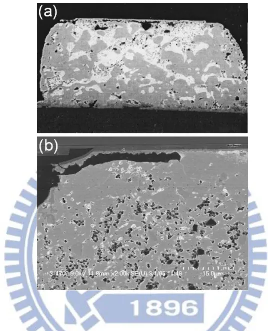
Figure 1-1 (a) A tilt-view of SEM image of arrays of solder bumps on silicon die. (b) A flip-chip solder joint to connect the chip side and the module side. (c) The chip placed upside down (flip chip), and all the joints are formed simultaneously between chip and substrate by reflow [1,5]...24 Figure 1-2 (a) Blech’s pioneering electromigration sample, showing an aluminum strip deposited on a conducting TiN layer. (b) An SEM image of the morphology of a Cu strip tested for 99 h at 350 °C with current density of 5 105 A/cm2
[16,18]...25 Figure 1-3 A schematic diagram of two-dimensional conductor film with grain boundary and intersection [18]...26 Figure 1-4 (a) The unique line to bump geometry of a flip-chip solder bump joining to a interconnect line on the chip side (top) and a conducting trace on the substrate side (bottom). (b) The two-dimensional simulation of current density distribution in a solder joint [16,42]...27 Figure 1-5 (a) The SEM image of a sequence of void formation and propagation in a flip-chip eutectic SnPb solder bump stressed at 125 °C and 2.25 × 10⁴ A/cm2 for 40 h. (b) The SEM image of void formation in a flip-chip 95.5Sn-4.0Ag-0.5Cu solder bump stressed at 146 °C and 3.67 × 10³ A/cm2 [24,25]...28
xiii
Figure 1-6 Plot of carbon content (logarithmic scale) vs. 1/T for sectioned alpha iron specimen [26]...29 Figure 1-7 The formation of voids on the chip side and accumulation of solder on the substrate side for the solder bump with (a) downward electron flow and (b) upward electron flow [27]...30 Figure 1-8 (a) A cross section of a composite 97Pb3Sn and 37Pb63Sn flip-chip solder joint. (b) The SEM image of the cross section. The darker region at the bottom is the eutectic SnPb. The brighter region is the 97Pb3Sn phase [37,42]...31 Figure 1-9 (a) A schematic diagram depicting 24 bumps on the periphery of a Si chip. Each bump has its original microstructure, as shown in Figure 1-9(b), before EM stressing. EM was conducted at 1.6 × 10⁴ A/cm2 at 150 °C through only four pairs of bumps on the chip’s periphery: pairs 6/7, 10/11, 14/15, and 18/19. (b) TM affected all the un-powered solder joints: The darker eutectic phase moved to the hot Si side [37]...32 Figure 1-10 SEM images of cross-sectioned bump with markers before and after TM test at 1.01× 10⁴ A /cm2 and 100 °C. (a) Before TM, and (b) After 800 h of the TM test. The markers moved toward the substrate side [38]...33 Figure 1-11 (a) Cross-sectional SEM images representing the microstructure for an un-powered bump before a TM test. (b) Temperature distribution measured by an
xiv
infrared microscope when the neighboring bumps were stressed by 0.55A at 150 °C. The built-in thermal gradient was 1143°C/cm across the solder bump. (c) After the TM test for 60 h. The Cu UBM was dissolved [42]...34 Figure 2-1 Schematics of the flip-chip solder joints with (a) a Ni UBM and (b) a Cu column UBM in this study...50 Figure 2-2 The simulation model for one pair of the flip-chip solder joints. The arrows show the direction of the electron flow...51 Figure 2-3 Cross-sectional SEM images of a solder bump with a 2-μm Ni UBM stressed at 2.16 × 10⁴ A/cm2 at 150 °C for (a) 0 h, (b) 42.7 h with upward electron flow, (c) EDS analysis at the point A in (b), and (d) 42.7 h with downward electron flow...52 Figure 2-4 Cross-sectional SEM images of a solder bump with a Cu column UBM stressed at 2.16 × 10⁴ A/cm2 at 150 °C for (a) 0 h, (b) 286.5 h with upward electron flow, and (c) 286.5 h with downward electron flow...53 Figure 2-5 Simulation results for current density distribution in the solder bump with a 2-μm Ni UBM when powered by 1.5 A...54 Figure 2-6 Simulation results for the current density distribution in (a) the Cu column UBM and (b) the solder bump beneath when powered by 1.5 A...55 Figure 2-7 Temperature increases in solders with 2-μm Ni UBMs and Cu column
xv
UBMs during current stressing as a function of applied currents and current density...56 Figure 2-8 IR images showing the temperature distribution in solder bumps with (a) a 2-μm Ni UBM and (b) a Cu column UBM during current stressing of 2.30 × 10⁴ A/cm2 at 100 °C...57 Figure 2-9 (a) The temperature profile along the AB line in Figure 2-8(a). (b) The temperature profile along the CD line in Figure 2-8(b)...58 Figure 3-1 Cross-sectional schematic structure of (a) the electromigration tests layout design and Kelvin bump probe structure for measuring bump resistance and (b) the solder joint configuration used in this study...69 Figure 3-2 Cross-sectional SEM image showing the microstructure of the solder joint after current stressing by (a) 1.15 × 10⁴ A/cm2 at 133.2 °C for 474.7 h and (b) 5.3 × 10³ A/cm2 at 175.3 °C for 83.2 h...70 Figure 3-3 Schematic drawing of a solder joint subject to a downward electron flow...71 Figure 3-4 The calculated curves for the Sn EM and chemical potential fluxes stressed by (a) 1.15 × 10⁴ A/cm2 at 125 °C and (b) 5.3 × 10³ A/cm2 at 175 °C as a function of time...72 Figure 4-1 (a) Schematic diagram for the solder joint structure used in this study. (b)
xvi
Cross-sectional SEM images showing the as-reflowed SnPb composite solder joint. (c) SEM image showing the FIB-polished second cross-section of the as-fabricated solder bump...85 Figure 4-2 (a) and (b) Cross-sectional SEM images showing the solder bump after 500 cycles of TCT. (c) SEM image showing the FIB-polished second cross-section of the solder bump after 500 cycles of TCT...86 Figure 4-3 (a) and (b) Cross-sectional SEM images showing the solder bump after 1500 cycles of TCT. (c) SEM image showing the FIB-polished second cross-section of the solder bump after 1500 cycles of TCT...87 Figure 4-4 (a) and (b) Cross-sectional SEM images showing the solder bump after 14410 cycles of TCT. (c) SEM image showing the FIB-polished second cross-section of the solder bump after 14410 cycles of TCT...88 Figure 4-5 Cross-sectional SEM image and SEM image showing the FIB-polished second cross-section of the solder bump after an isothermal annealing at 150 °C for (a), (b) 500 h, (c), (d) 1000 h, and (e), (f) 2160 h...89 Figure 4-6 The average IMCs thickness as a function of time...90 Figure 4-7 Simulation results for the total mechanical and thermal equivalent strain distribution in (a) the solder bump and (b) the Sn63Pb37 presolder after one cycle of TCT...91
xvii
Figure 4-8 Simulation results for the hydrostatic stress distribution in the solder bump at (a) -55 °C and (b) 125 °C...92
1
Chapter 1 Overview of interfacial reaction, electromigration,
thermomigration
and
stress
migration
in
flip-chip
technology
1.1 Flip-chip technology
To meet the relentless demand for miniaturization of portable devices, flip-chip technology has been adopted for high-density packaging due to its excellent electrical characteristic and superior heat dissipation capability [1]. As the required performance in microelectronics devices becomes higher, flip-chip technology was adopted to increase more signal and power interconnections than wire bonding in electronic devices. In 1960s, IBM first developed the flip-chip technology, called as controlled-collapse-chip-connection (C4) [2-4]. In the C4 technology, high-Pb solder with high melting temperature of 320 °C was used as the joint material [5]. Then the chip was aligned on the ceramic substrate. This C4 technology gained wide utilization in the 1980s since it can provides the advantages in size, performance, flexibility, and reliability over other packaging methods. Owing to the area array capability in flip-chip technology, the size of product, the height of solder bump, and the length of interconnect are effectively reduced, the higher input/output (I/O) pin count and speed in electronic devices was provided.
2
Before flip-chip assemblies, solder bumps need to be deposited onto the under-bump-metallization (UBM) on the chip side. The requirements for UBMs are: (1) it must adhere well both on the underlying metal line, like Al or Cu, and on the surrounding IC passivation layer, (2) it is able to provide a strong barrier to prevent the diffusion of bump metals into the integrated circuit (IC) and (3) it needs to be readily wettable by the bump metals during solder reflow. For example, a thin film Cr/Cu/Au UBM is adopted for the high-Pb solder alloy in the C4 technology.
The tilt view of solder joints on silicon chip is shown in Figure 1-1(a). Figure 1-1(b) is the cross-sectional view of the flip-chip solder joints. As depicted in Figure 1-1(c), the chip with IC is then placed upside down (flip chip), and all the joints are formed simultaneously between chip and substrate during the reflowing process. In flip-chip process, electrical connections are the array of solder bumps on the chip surface, hence interconnects distance between package and chip is effectively reduced. The density of I/O is limited by minimum distance between adjacent bonding pads. For high ends device, when size reduction is the main concern, area-arrayed flip-chip technology is the only choice to meet the needs.
However, the flip-chip technology has some evolutions due to certain concern. In order to cost down the consumer electronics, the polymer substrates, like Bismaleimide Triazine (BT) or Flame Retardant 4 (FR4), are used to replace the
3
ceramic substrate. For this concern, the high-Pb solder has no longer been used due to its high melting point of 320 °C since polymers have very low glass transition temperature. Thus, the eutectic SnPb solder alloy can been used to solve this problem by its low melting point of 183 °C. Next, owing to the environment concern, the Pb-free solder alloys replace the Pb-containing solder alloys due to the toxic of Pb. Then, the thin film UBM will not be suitable for this change. Therefore, the electroplating 5-m Cu or 5-m Cu/3-m Ni was used as the UBM for the Pb-free solder joints. Because of these evolutions, several kinds of solder alloys and UBMs are proposed for the flip-chip assemblies. This makes the flip-chip technology become complex to study since there has too many combinations. The best solder alloy and UBM will provide a lot of benefit for the industry.
1.2 Interfacial reaction
Solder is widely used to connect chips to their packaging substrates in flip-chip technology as well as in ball-grid-array (BGA) technology [6]. In the last 50 years, the electronics industry has relied mainly on one type of solder (Sn–Pb solder) in products manufacture [7]. With the discovery of Pb as a contaminant both to the environment and to human health, new developments have been made to steer away from the use of Sn–Pb solder [8,9]. In 2000, National Electronics Manufacturing
4
Initiative (NEMI) recommended to replace eutectic Sn–Pb solder by eutectic Sn–Ag– Cu solder in reflow processing and eutectic Sn–Cu solder in wave soldering [6].
A reliable solder joint can be formed by metallurgical reactions between molten solders and UBM on a chip or metallization on the substrate, which produces stable intermetallic compounds (IMCs) at the joint interfaces [10]. During the soldering process, the formation of IMCs between solder alloys and the metallization layer is inevitable. The growth of these IMCs can strongly affect the mechanical reliability of the solder joints [11-13]. As a result, selection of appropriate UBMs plays an important role in developing a reliable flip-chip solder joint, especially the adoption of the lead-free solders due to environmental concerns.
Copper is widely used in the UBM and substrate metallization for flip-chip and BGA applications. It is known that at the Cu/solder interface, Sn reacts rapidly with Cu to form Cu–Sn IMC, which weakens the solder joints due to the brittle nature of the IMC [14]. Therefore, Ni is used as a diffusion barrier layer to prevent the rapid interfacial reaction between solder and Cu layer in electronic devices.
Recently, the reaction between solder and Ni has received much attention because the reaction rate is about two orders of magnitude slower than that of Cu, so the effect of spalling of IMC on thin film Ni is less serious and Ni can also serve as diffusion barrier. Why the reaction rate between Ni and solder is much slower than
5
that between Cu and solder has been an interesting kinetic question. The answer is not very clear right now; mostly it is because the supply of Ni to the reaction that may be much slower than Cu. The supply may depend on the diffusion of Ni along the interface between Ni3Sn4 and Ni and also the solubility of Ni in the molten solder
[15].
1.3 Electromigration
Electromigration (EM) is the phenomenon of mass transportation due to momentum transfer from high current density. Such a mechanism can result in open or short circuit modes of failure. The mechanism also impacts both the design and manufacturing of metallization. For electromigration in a metal, the driving force of the net atomic flux consists of two forces: (1) the direct action of electrostatic field on the diffusion atom, electrostatic force, and (2) the momentum exchange between the moving electrons and the ionic atoms on the diffusion atom, electron wind force. It can be expressed as
( ) (1-1) where is the effective charge number, e is the electron charge, and E is the electric field. The effective charge is consisted of two terms, and . is positive and can be regarded as the nominal valence of the diffusion ion in the metal
6
when the dynamic screening effect is ignored. When these positively charged metal ions are under the field effect, this so called ―direct force‖ draws atoms towards the negative electrode. In the contrary, the wind force, is usually negative and represents the momentum effect from electron flow that pushes atoms towards the positive electrode. Generally, the electron wind force dominates and is found to be on the order of 10 for a good conductor like Ag, Al, Cu, Pb, Sn, etc [16]. can also be positive, but it was found only in transition elements with complex band structures where electron hole conduction plays a more important role [17]. The atomic flux is related to the electric field and thus the current density. The flux equation can then be expressed as the following:
𝐽 𝐽 𝐽 (1-2)
(1-3) where C is atomic concentration, D is atomic diffusivity, k is Boltzmann’s constant, and T is temperature. is resistivity and j is current density. The flux is a function of temperature. As shown in the equation below, the atomic diffusivity is exponentially dependent on temperature.
( ) (1-4) where is diffusion coefficient, R is gas constant, and Q is activation energy of diffusion.
7
For electromigration to occur, a nonvanishing divergence of atomic flux is a requirement. The divergence may be due to a temperature gradient or microstructural inhomogeneity. Since electromigration is cumulative, it affects the failure rate. Therefore, the mean time to failure (MTTF) in the presence of electromigration is given by the equation
( ) (1-5) The electromigration exponent ranges from n=1 to n=6, i.e. n=2 for Al interconnect. The failure mechanism results in voids, cracks, and hillocks in the samples.
1.3.1 Failure sites and flux divergence
Electromigration was first observed in Al metal interconnects. Less than 0.2% Cu atoms were added to Al line to reduce the effect of electromigration [16]. Blech first developed a structure of a short Al or Cu strip in a base line of TiN to conduct electromigration tests as shown in Figure 1-2(a) [18,19]. Because Al or Cu has lower resistance, as electric field was applied on two ends of TiN line, electric current in TiN took a detour to go along the strip of Al or Cu. After electromigration test, a depleted region occurs at the cathode and an extrusion is observed at the anode. Figure 1-2(b) is the scanning electron microscope (SEM) image of the morphology of
8
a Cu strip tested for 99 h at 350 °C with a current density of 5 105
A/cm2. By conservation of mass, both depletion and extrusion should have the same volume change. We can then calculate the drift velocity from the rate of depletion. In the past years, an impetus to study electromigration in very fine conductors has arisen from the development of very large-scale integrated circuits. The conductors are not only interested in small dimensions; they are often assembled into multilayered structure with a certain combination of conductors and insulators. This gives rise to electromigration problems which is distinctly different from simple single-level conductor line.
The metal layer is a two-dimensional (2D) conductor film that can be considered as an ensemble of grain boundaries and their intersections as illustrated in Figure 1-3. Experimental observations have indicated that in most cases, mass depletion and accumulation initiate at grain boundary intersection such as triple junctions. The former would eventually lead to the formation of voids or cracks and the latter to hillocks or whiskers. The reason that the grain boundary intersections are likely to be the failure sites is that they often represent the spots where the mass flux would diverge the most. At the grain boundary intersections, there could be an abrupt change in grain size, which produces a change in the number of paths for mass movement; there also could be a change in atomic diffusivity due to the change in grain boundary
9
microstructure.
Recently damascene structure have been developed to form Cu interconnect. Cu material is used to replace Al due to its higher electrical conduction. Because Cu has higher melting temperature, its diffusion mechanism is surface diffusion instead of grain boundary diffusion [20]. As for solder joints, because it has lower melting temperature, the diffusion mechanism is lattice diffusion for most solders at a typical operation temperature of an electronic device around 100 °C. Table 1-1 lists the melting temperature of Al, Cu, SnPb solder, and their corresponding diffusion mechanism.
1.3.2 Current crowding effect
Within a metal line, as soon as the electromigration-induced damage forms, current density also becomes non-uniform. As voids or cracks grow, the non-uniformity of the current density over a conductor line increases. Since the Joule heating is proportional to the square of the current density, the local temperature will also increase rapidly. The current crowding effect therefore plays dual roles here: both the elevated local density and temperature accelerate the electromigration process. Thus obtaining an accurate current crowding density distribution is necessary in determining the flux divergence [20].
10
Current crowding phenomenon is an even more serious issue in flip-chip solder joints. Figure 1-4(a) demonstrates the unique line to bump geometry of a flip-chip solder bump joining an interconnect line on the chip side (top) and a conducting trace on the substrate side (bottom) [17,21,22,23]. Because the cross section of the line on the chip side is about two orders of magnitude smaller than that of a solder joint, the current density changes significantly from the metal line to the solder as current enters the solder joint. The change leads to the current crowding at the entrance into the solder bump, thus resulting in the change of magnitude of current density from 105 A/cm2 to 104 A/cm2 at the current crowding region in a typical Al line to solder bump structure. Figure 1-4(b) is a 2D simulation of current distribution in a solder joint. Note that this current crowding phenomenon leads to non-uniform current distribution inside a solder joint. The current density at the current crowding region is one order of magnitude higher than the average current density at the center of the solder joint. Since the drift velocity is proportional to the current density and non-uniform temperature distribution inside a solder joint due to local Joule heating effect (see Section 1.3.3), electromigration-induced damage occurs near the contact between the on-chip line and the bump; voids formation for the bumps with electrons downward and hillock or whisker for the bumps with electrons upward. Therefore, current crowding effect plays a crucial role in the flip-chip solder joints under
11
electromigration. Consequently, electromigration damage occurs near the contact between the line and the bump; voids induced from the damage can propagate along the interface due to the non-uniform current distribution [24].
In those flip-chip solder joints using a thin film UBM, the current crowding leads to a pancake-type void across the entire cathode contact [25,26]. Figure 1-5(a) displays the SEM images of eutectic SnPb after electromigration [24]. After current stressing for 40 h at 125°C and 2.25 × 10⁴ A/cm2, voids are seen in the left-upper corner since electron flow entered the bump from the upper-left corner of the joint. Similar phenomena were also observed in Sn-4.0Ag-0.5 Cu Pb-free solder joints as shown in Figure 1-5(b) [25]. Pancake-type void is clearly seen at the corner of flip-chip solder joints when the cathode is on the chip side. With current stressing time increases, pancake-type voids propagate across the top of solder joints, resulting in open failure.
1.3.3 Joule Heating Effect
When the current flow passes through a conductor, the heat generated due to the electrons vibrating the atoms in the conductor. This is so called Joule heating effect. The heating power can be describe as:
12
where P is heating power, I is applied current, R is resistance of the conductor, j is current density, is resistivity of the conductor, and V is volume of the conductor. Thus, the heating is controlled by two factors: first is the applied current, and the other is the resistance of the conductor.
When the current applied to a flip-chip solder joint is relatively high, the whole system will generate a huge amount of heat resulting from the conducting traces and solder bumps. Generally, the total length of the Al trace can reach few meters, which the effective resistance is approximately few ohms. In contrast, the resistances of the solder bumps and the Cu trace on the substrate are relatively low, typically in the order of few or tens of milliohms. Therefore, the major contribution for Joule heating in flip-chip solder joints comes from the Al trace [27-29]. As a result, the temperature in the bumps during accelerated testing is likely to be much higher than that of the ambient because of the Joule heating. Moreover, the current crowding effect will cause the local high current density; in other words, there will be a local Joule heating in the solder joints and result in a non-unformed temperature distribution. Chiu et al reported the ―hot spot‖ exists inside the solder bumps at the current crowding region [29,30]. The combination of the Joule heating of Al interconnects on the chip side and the non-uniform current distribution will lead to a temperature gradient across the solder joints. Consequently, Joule heating effect induced temperature increase in the
13
flip-chip solder joints under electromigration significantly affects the analysis of failure time.
1.3.4 Mean time to failure
Electromigration requires a nonvanishing divergence of atomic flux. Since electromigration is cumulative, it affects the failure rate. In statistical study, the test samples should be stressed at the same current and temperature conditions. Then, the failure times or lifetimes can be recorded and plot by Weibull or normal distribution. In Weibull distribution, the time of 63.2% of reliability is denoted as the mean-time-to-failure (MTTF) [31]. In 1969, James R. Black explained the MTTF in the presence of electromigration is given by the equation [32]:
( ) (1-5) where A is a constant, j is the current density, n is a model parameter, Q is the activation energy, k is the Boltzmann’s constant, and T is the average temperature. There are four of parameters: j, n, Q, and T needed to be examined and analyzed. However, the current crowding effect and the Joule heating effect play important roles under electromigration in flip-chip solder joints. To further consider about these two effects in MTTF analysis, the modified Black’s equation becomes:
14
by multiplying j with a crowding ratio c and adding an increment of T due to Joule
heating [33]. For the following discussion, the estimated MTTF will be a key result to compare to each other.
1.4 Thermomigration
Thermomigration (TM) is the flux of component in a solution induced by the temperature gradient. The phenomenon has also been called thermal diffusion. When a concentration gradient is established due to the impressed temperature, it is known as Ludwig-Soret Effect [26]. From the atomic point of view, temperature gradient can lead to the un-mixing of an initially homogenous alloy due to a biasing of the atomic jump [17]. Instead of electrical field, as in the case for electromigraiton, the effective driving force exerted by the temperature gradient is expressed as
(1-8) where Q* is the experimental determined parameter which describes the sign and magnitude of the thermo-transport effect. It is called the heat of transport of the component. Q* is positive in the flux equation when the flux is from hot to cold region. For situation in which one component is diffusing, e.g. an interstitial alloy, the flux equation is then given as [27, 39]
15
D/kT is the mobility of the diffusing component, and dC/dx is the concentration
gradient at constant temperature. Note that D is the diffusion coefficient. The temperature gradient does not change the jump mechanism or mean jump frequency at any given temperature. However, it biases the direction of jump.
1.4.1 Measurement of the heat of transport
Q* can be obtained by two methods. One method is to allow flux to go to zero in
a temperature gradient and measure the concentration gradient at J=0. The other method is to measure the flux through an open system at a known temperature gradient. Figure 1-6 demonstrates the concentration of carbon content in an initially single-phase alloy (0.01%C) under a temperature gradient until a steady state was established. Note the final concentration gradient across the specimen is a linearly relationship with temperature and concentration becomes higher at the hot end. With the flux equals to zero, equation (1-9) becomes
𝐶1 1 2 (1-10)
The method allows Q* to be obtained from the slope of the curve without any information on the diffusion coefficient. In the case of the α-Fe shown in Figure 1-6, 𝑄 96 kJ/mol. It means carbon moves toward the hot end.
16
highly affected by the change in the equilibrium vacancy with temperature. The flux of the element under a temperature gradient can be expressed as
𝐽 𝐴 𝛺 ( 𝐴−𝐻𝜐) 2 (1-11)
where 𝛺 is atomic volume and 𝐻𝜐 is enthalpy of formation of vacancies. 𝑄𝐴 is heat of transport for element A. Experiments have been done by heating one end of pure metal and cooling the other end or by heating the center of a sample by passing an electric current through it and keeping the end cold. The net flux of atom is then measured by the motion of inert marker relative to the end of the sample. Table 1-2 [34] lists the experimental values of 𝑄𝐴 for several pure metals. All the values for 𝐻𝜐 are invariably larger than 𝑄𝐴 so the vacancy concentration gradient dominates and the net flux of vacancies is always toward the cold end. As a result, more vacant sites at the hot end allow atoms to jump into on its higher temperature side than on its lower temperature site. An increase in the distance between markers in the hottest parts of the sample is observed [17]. Since the effect of 𝑄𝐴 is small relative to the vacancy gradient effect, 𝑄𝐴 cannot be measured with much accuracy. The situation becomes even more complex when it becomes binary alloys. Whether one element becomes enriched at the hot end or cold end of the sample is determined by the competition between the flows of the two elements relative to the lattice under the temperature gradient.
17
1.4.2 Thermomigration accompanying electromigration in flip-chip solder joints
Thermomigration has been reported to accompany electromigration in flip-chip solder joints recently [35,36]. The major heat source exerted on solder joints is from Al trace on the Si die side. Longer electric current path and high current density in Al trace increase the temperature of the Si chip tremendously. As a result, a temperature gradient existed across solder joints and thermomigration can occur along with electromigration. Figures 1-7(a) and (b) show the SEM images of an example of a pair of eutectic SnPb solder joints after current stressing. The sample was finely polished to half of the bump before the testing. Figure 1-7(a) shows the formation of the voids on the chip side and accumulation of solder on the substrate side for the solder bump with downward electron flow. However, as shown in Figure 1-7(b), for the solder bump with upward electron flow, voids were also observed on the chip side. This phenomenon cannot be explained by electromigration since the atomic movement is against electron flow on the chip side. It is due to the competing effect of electromigration and thermomigration, as further proved by the marker movement. From temperature measurement and simulation, it was estimated that a temperature difference of 15 °C generated across a solder joint of 100 m in diameter, and the temperature gradient of 1500 °C/cm seems sufficient to cause thermomigration in eutectic SnPb solder joints.
18
1.4.3 Thermomigration in composite SnPb flip-chip solder joints
The combination effect of electromigration and thermomigration was observed for powered bump. When the electronic device is large and thermal dissipation is sufficient on the Si chip, signal bump or unpowered bump has minimal thermal effect. However, when the electronic device and bump pitch become smaller, thermal effect from the powered bump can no longer be neglected.
To induce thermomigration in the composite solder joints, we used the temperature gradient induced by Joule heating in electromigration test. A set of flip-chip samples is depicted in Figure 1-8(a) [37], wherein there are 24 bumps on the periphery of a Si chip, and all the bumps have their original microstructure, as shown in Figure 1-8(b), before electromigration stressing. After electromigration was conducted through only four pairs of bumps—pairs 6/7, 10/11, 14/15, and 18/19 in Figure 1-9(a), thermomigration affected all the unpowered solder joints, as shown in Figure 1-9(b). All the Sn (the darker image) migrated to the hot Si side, whereas the Pb migrated to the cold substrate side. The redistribution of Sn and Pb was caused by the temperature gradient across the solder joints because no current was applied to them. Since Si has a very good thermal conductivity, the Joule heating of Al interconnects on the chip side of the four pairs of powered bumps has heated the
19
entire Si chip to induce a temperature gradient and in turn the thermomigration across all the unpowered bumps.
1.4.4 Thermomigration in Pb-free flip-chip solder joints
Hsiao et al. [38] performed thermomigration by operating with alternating current (AC) and direct current (DC). The advantage of AC is that there would be no electromigration under AC, and this will be a good way to decouple electromigration and thermomigration. The schematic diagram of a Pb-free solder bump used in thermomigration study is shown in Figure 1-10(a). After 800 h of 1.01× 10⁴ A/cm2 current stressing at 100 °C, hillocks are present on the chip side, as shown in Figure 1-10(b). The hillocks are formed by the mass transfer in the solder bump caused by thermomigration and comprised of Sn confirmed using a SEM energy dispersive spectroscopy (EDS). This result reveals that Sn atoms are driven from cold side to the hot side under thermomigration.
Moreover, during electrmigration test which will couple with thermomigration, not only solder (Sn or Pb) will affect but also UBMs. The dissolution of Cu and Ni in Pb-free solders is quite high, and the diffusion of Cu and Ni in Sn is anisotropic and very fast. The diffusion rate along the c-axis of Sn crystals is faster than that in the a- and b-axis. The dissolution of Cu and Ni atoms may occur under a thermal gradient
20
[39]. Figure 1-11(a) shows a eutectic SnAg solder bump with a 5-μm UBM on the chip side before a TM test. This bump was next to a bump that was under EM stressing at 0.55 A and 150 °C. This joint had no current passing through it but possessed a thermal gradient of 1143 °C/cm, as illustrated in Figure 1-11(b). After 60 h of the TM test, the Cu-Sn IMC migrated to the cold (substrate) end, as shown in Figure 1-11(c). Although this bump was un-powered, the damage is clear near the upper left corner, as indicated in Figure 1-11(c). The Cu UBM dissolved almost completely into the solder. This dissolution can be attributed to the TM of Cu atoms by fast interstitial diffusion and the reaction with Sn atoms to form Cu-Sn IMCs inside the solder bump.
1.5 Stress migration
At high homologous temperatures and low stresses polycrystalline materials deform by diffusional creep. Material redistribution during the creeping process can either occur as the result of the diffusional transport of material through the grains or along the grain boundaries. Nabarro originally described the process of creep deformation by lattice diffusion, and a general framework for analyzing diffusive mechanisms was developed by Herring [40,41]. According to Nabarro-Herring model of creep, atomic flux will diffuse from the compressive region to the tensile region.
21
The atomic flux is related to the stress gradient, and the flux equation can then be expressed as the following:
𝐽 𝛺 (1-12) where C is the concentration, D is the atomic diffusivity, kT has the usual meaning, Ω is the atomic volume, and dσ/dx is the stress gradient. When crystalline solids are tested under creep conditions at low stresses and high homologous temperatures, the creep rates vary linearly with the applied stress so that strain is accumulated through the processes of Nabarro-Herring creep, and how the stress migration affect the evolution of the microstructure in the solder joints will be discussed later.
1.6 Motivation
In this thesis, we study the electromigration behavior and the stress migration behavior in the solder joints. When the system is subject to electromigration, thermomigration, and stress migration, the overall flux can be expressed in terms of chemical force, electrical wind force, thermal gradient, and stress gradient as the following:
𝐽 2 𝛺 (1-13) Detailed discussion on the contribution of each term will be reported in the later chapters.
22
Table 1-1 Melting temperature, diffusivity and diffusion mechanism for Cu, Al, Pb and SnPb solder [16].
4
23
24
Figure 1-1 (a) A tilt-view of SEM image of arrays of solder bumps on silicon die. (b) A flip-chip solder joint to connect the chip side and the module side. (c) The chip placed upside down (flip chip), and all the joints are formed simultaneously between chip and substrate by reflow [1,5].
25
Figure 1-2 (a) Blech’s pioneering electromigration sample, showing an aluminum strip deposited on a conducting TiN layer. (b) An SEM image of the morphology of a Cu strip tested for 99 h at 350 °C with current density of 5 105
26
Figure 1-3 A schematic diagram of two-dimensional conductor film with grain boundary and intersection [18].
27
Figure 1-4 (a) The unique line to bump geometry of a flip-chip solder bump joining to a interconnect line on the chip side (top) and a conducting trace on the substrate side (bottom). (b) The two-dimensional simulation of current density distribution in a solder joint [16,42].
28
Figure 1-5 (a) The SEM image of a sequence of void formation and propagation in a flip-chip eutectic SnPb solder bump stressed at 125 °C and 2.25 × 10⁴ A/cm2 for 40 h. (b) The SEM image of void formation in a flip-chip 95.5Sn-4.0Ag-0.5Cu solder bump stressed at 146 °C and 3.67 × 10³ A/cm2 [24,25].
29
Figure 1-6 Plot of carbon content (logarithmic scale) vs. 1/T for sectioned alpha iron specimen [26].
30
Figure 1-7 The formation of voids on the chip side and accumulation of solder on the substrate side for the solder bump with (a) downward electron flow and (b) upward electron flow [27].
31
Figure 1-8 (a) A cross section of a composite 97Pb3Sn and 37Pb63Sn flip-chip solder joint. (b) The SEM image of the cross section. The darker region at the bottom is the eutectic SnPb. The brighter region is the 97Pb3Sn phase [37,42].
32
Figure 1-9 (a) A schematic diagram depicting 24 bumps on the periphery of a Si chip. Each bump has its original microstructure, as shown in Figure 1-9(b), before EM stressing. EM was conducted at 1.6 × 10⁴ A/cm2 at 150 °C through only four pairs of bumps on the chip’s periphery: pairs 6/7, 10/11, 14/15, and 18/19. (b) TM affected all the un-powered solder joints: The darker eutectic phase moved to the hot Si side [37].
33
Figure 1-10 SEM images of cross-sectioned bump with markers before and after TM test at 1.01× 10⁴ A /cm2 and 100 °C. (a) Before TM, and (b) After 800 h of the TM test. The markers moved toward the substrate side [38].
34
Figure 1-11 (a) Cross-sectional SEM images representing the microstructure for an un-powered bump before a TM test. (b) Temperature distribution measured by an infrared microscope when the neighboring bumps were stressed by 0.55A at 150 °C. The built-in thermal gradient was 1143°C/cm across the solder bump. (c) After the TM test for 60 h. The Cu UBM was dissolved [42].
35
Chapter 2 Influence of Cu column UBMs on current
crowding and Joule heating effects of electromigration in
flip-chip solder joints
2.1 Introduction
For high-density packaging, the application of flip–chip solder joints has become the most important technology in the microelectronic industry [16]. To accommodate the performance requirement of portable devices, the number of input/output (I/O) continues to increase and the size of the joints continues to shrink. This trend has been accounted for the increase in current density and temperature rise in solder joints, and also known as the current crowding effect and Joule heating effect, respectively. Accordingly, these two effects cause serious reliability issues in flip-chip solder joints such as electromigration and thermomigration [42].
Several studies about electromigration of flip-chip solder joints have been reported [24,29,33,35,43-46]. Current crowding especially has strong effect at the entrance spot of the Al trace into the solder joint, thus the main factor responsible for the failure near the chip/anode side in most solder joints [24,44]. On the other hand, Joule heating effect also occurs during accelerated electromigration tests [29,33,35,45,46]. The temperature increase due to Joule heating effect may be over 30
36
C when a solder bump is stressed by a 1.0 A current [33,35,44]. Therefore, Cu column UBM, a structure with a thick UBM, was developed to alleviate both the current crowding and Joule heating effect in flip-chip solder joints under normal operating conditions [47]. The operating temperature may affect the MTTF significantly, as depicted by Black’s equation [32]:
) kT Q ( exp j 1 A MTTF n (2-1) where A is a constant, j is the current density in amperes per square centimeter, n is a model parameter for current density, Q is the activation energy, k is Boltzmann’s constant, and T is the average bump temperature in degrees Kelvin.
Only few studies have been reported on the EM failure mechanism for solder joints with Cu column UBMs [48-50]. Nah et al. reported electromigration in flip-chip solder joints with 50-μm thick Cu columns and they found that the Cu columns can relieved the current crowding effect in solder [48]. Lai et al. investigated the MTTF and failure mechanism of electromigration in solder joints with 62-μm thick Cu columns, and they found the MTTF of the joints was enhanced by the thick Cu columns [49]. Xu et al. reported that electromigration accelerated the consumption rate of the Cu columns and transformed almost the entire solder into IMCs [50]. However, no study addresses the Joule heating effect of the solder joints with Cu UBMs. In this study, we investigate EM failures in the solder bumps with 64-μm thick
37
Cu column UBMs. Electromigration tests were also performed in solder joints with 2-μm thick Ni UBMs for comparison. The wiring circuits are the same for both sets of solder joints. Therefore, this study provides a direct comparison on the failure mode and thermo-electrical characteristics between regular solder joints and the solder joints with Cu column UBMs.
2.2 Experimental procedure
In order to investigate the influence of Cu columns on current crowding and Joule heating effects, two types of flip chip solder joints were tested: one type has traditional solder joints with 2-μm-thick Ni UBMs and one type has an addition of 64-μm-thick Cu column UBMs followed by a coated layer of 4-μm-thick Ni layer.
The test vehicles were 13.5 × 13.5 × 1.39 mm flip-chip packages, which involve a 3.8 × 3.8 × 0.73 mm silicon chip interconnected to a substrate. The pitch between adjacent solder joints was 270 μm. The diameter of UBM opening and passivation opening were 110 μm and 90 μm, respectively. Printed solder of Sn-2.6Ag and Sn-3.0Ag-0.5Cu solder were formed on the chip side. The substrate pad metallization features the solder on pad (SOP) surface treatment, i.e., with printed Sn-3.0Ag-0.5Cu pre-solder on the Cu pad surface. The printed solder and the SOP were then reflowed together to become lead-free solder bumps as schematically shown in Figures 2-1(a)
38
and 2-1(b). For electromigration tests, the stressing condition was 2.16 × 10⁴ A/cm2 at 150 °C.
Microstructure and composition were examined by a JEOL 6500 field-emission SEM and EDS, respectively. The IMC of (Cu,Ni)6Sn5 was formed at the interface of
the Ni layer and the solder on the chip side while Cu6Sn5 without Ni dissolution was
formed at the interface of the solder and the Cu metallization layer on the substrate side. In addition, Ag3Sn IMCs were formed dispersedly in the solder bumps.
To investigate the Joule heating issue during current stressing, infrared (IR) microscopy was employed. Solder joints are completely enclosed by a Si chip, underfill, and a polymer substrate so it is difficult to examine the temperature inside solder joints directly. To overcome this difficulty, samples were polished laterally close to a point near the centers, and the temperature distribution inside the solder bump was measured directly by an IR microscope at various stressing conditions. Prior to current stressing, the emissivity of the specimen was calibrated at 100 °C. After calibration, solder joints were powered by a desired current. Temperature measurement was then performed to record the temperature map distribution at a constant rate. The temperatures in the solder joints were mapped by a QFI thermal infrared microscope, which has 0.1 °C temperature resolution and 2-μm spatial resolution.
39
2.3 Simulation
Three-dimensional (3D) finite element analysis was employed to simulate the current density distribution in the solder joints. The model included two solder joints, an Al trace, and two Cu lines as shown in Figure 2-2, and the direction of the electron flow was shown by two of the arrows. The dimensions of the Al trace, pad opening, and the Cu line were identical to the real flip-chip samples. The IMCs formed between the UBM and the solder were also considered in the simulation models. Layered IMCs of Cu6Sn5 were used in this simulation to avoid difficulty in mesh. The
resistivity values of the materials used in the simulation are listed in Table 2-1. The resistivity of Sn-2.6Ag cannot be found in literature. Thus, we adopted the resistivity of Sn-3.0Ag-0.5Cu for the solder, which should be very close to the resistivity of Sn-2.6Ag. The model used in this study was SOLID5 8-node hexahedral coupled field element using ANSYS simulation software.
2.4 Results and discussion
2.4.1 Electromigration failure site and failure mechanism change
The case without a Cu column UBM is presented here first. Figure 2-3(a) illustrates the cross-sectional SEM image of a solder bump with a Ni UBM before EM
40
tests. Figures 2-3(b) and 2-3(d) show the cross-sectional SEM images of solder bumps with Ni UBMs after upward and downward current stressing of 2.16 × 10⁴ A/cm2 at 150 °C for 42.7 h, respectively. The current density was calculated based on the area of passivation opening on the chip side. Open failure occurred after 42.7 h of current stressing, and the damage in the Al trace between two solder bumps can be observed by IR microscopy. When the direction of electron flow was from the substrate side to the chip side as shown in Figure 2-3(b), some of the Cu metallization layer on the substrate side was consumed and reacted with solder to form Cu6Sn5 IMCs. A slight
amount of Cu6Sn5 IMCs in the solder bump near the substrate side was aligned with
the direction of electron flow because of electromigration effect in the solder joint. A crack formed along the chip/solder interface, which may be attributed to polishing during sample preparation for cross-sectional SEM observation. Additionally, some voids were observed in the Al trace on the chip side, as labeled in Figure 2-3(b). Some of voids were filled with Sn atoms. Figure 2-3(c) shows the EDS analysis for the location A in Figure 3(b), and the results indicated the element there was almost pure Sn. We will discuss this interesting point later. When the direction of electron flow was from the chip side to the substrate side as shown in Figure 2-3(d), the solder melted because of serious Joule heating effect. Furthermore, underfill layer was also damaged. However, the EM failure mode of the solder joints with Cu columns is quite
41
different. Figure 2-4(a) shows the cross-sectional SEM image of a solder bump with a Cu column UBM before EM tests. Figures 2-4(b) and 2-4(c) show the cross-sectional SEM images of solder bumps with Cu column UBMs after upward and downward current stressing of 2.16 × 10⁴ A/cm2 at 150 °C for 286.5 h, respectively. During this period of current stressing time, the total resistance, which includes two solder joints and Al trace, is raised by 50 mΩ from 145 mΩ to 195 mΩ. When the direction of electron flow was from the substrate side to the chip side as shown in figure 2-4(b), voids of about 84.7 μm long can be observed clearly at the interface of Cu6Sn5 IMCs
and the solder on the substrate side. The voids in the middle of solder may be attributed to reflow process. This crack was the main reason of resistance increase during the failure. Similar to the results in the solder joint with a 2-μm Ni UBM in Figure 2-3(b), extensive dissolution of Cu layer on the substrate side took place, resulting in the massive formation of the Cu-Sn IMCs in the solder. Yet, there was no voids found in the substrate side in Figure 2-3(b). Ke et al. reported two failure mechanisms may occur in solder joints with Cu UBM: void formation and Cu dissolution [51]. It is not clear at this moment that why voids did not form in the solder joints in Figure 2-3(b).
When the direction of electron flow was from the chip side to the substrate side as shown in figure 2-4(c), the IMCs at the interface of the Ni layer and the solder
42
became thinner whereas the IMCs at the interface of the solder and the Cu metallization layer on the substrate side became thicker because of the polarity effect. Void of about 28 μm long was formed at the top-right-hand corner in the solder bump, and some Kirkendall voids can be observed at the interface of Cu3Sn IMCs and the
Cu metallization layer on the substrate side. The Cu column and the Ni layer beneath remained intact within our experimental time frame.
2.4.2 Current crowding effect
Current crowding effect plays a crucial role in the electromigration failure of solder joints. Since the current density in the Al trace is typically one or two orders in magnitude larger than that in the solder, current crowding occurs at the entrance point of the Al trace into the solder joint. Figure 2-5 depicts the 3D simulation of the current density distribution in the solder bump with Ni UBMs. The applied current was 1.5 A from the chip side to the substrate side, which resulted in a current density of 1.54 × 10⁶ A/cm2 in the Al trace. The calculated average current density was 2.16 × 10⁴ A/cm2 based on the area of passivation opening on the chip side. However, due to the current crowding effect, the maximum current density inside the solder bump is as high as 7.8 × 10⁴ A/cm2 as shown in Figure 2-5.
43
obtained in the solder bump as shown in Figures 2-6(a) and 2-6(b). Same as in Figure 2-5, the applied current was 1.5 A from the chip side to the substrate side. The maximum current density in the Cu column is 1.0 × 10⁶ A/cm2. It can be seen that the current crowding effect still occurs in the Cu column UBM near the entrance of the Al trace into the solder joint. However, since Cu has a much higher melting point than the SnAg solder (Cu: 1084 °C; SnAg: 221 °C), there was little EM damage in Cu in the present stressing condition. The Cu column UBM is thick enough, therefore the solder is kept away from the current crowding region, and the maximum current density in the solder bump dramatically decreases to 4.0 × 10⁴ A/cm2, which is only 51% of the maximum current density inside the solder bump with the 2-μm Ni UBM. In other words, the current flow spreads out and becomes more uniform before reaching the solder bump when Cu column UBM is utilized. As a result, instead of locating on the chip side, the current crowding region in the solder bump with Cu column UBMs is actually located on the substrate side. This result agrees with the phenomenon observed in Figure 2-3(c) and Figure 2-4(b). The main electromigration-induced damage position in the solder bump moved from the chip side to the substrate side because of the existence of Cu column UBMs.
44
2.4.3 Joule heating effect
The existence of Cu column UBMs also has influence on the Joule heating effect in the solder bump. Current stressing was carried out at the temperature of 100 °C on a hotplate. Figure 2-7 shows the temperature increases in solders with 2-μm Ni UBMs and Cu column UBMs during current stressing as a function of applied currents and current densities. Current stress was applied to solder joints with the current density in the range of 2.88 × 10³ A/cm2 to 2.30 × 10⁴ A/cm2 in the passivation opening. Figures 2-8(a) and 2-8(b) show the temperature distribution of the cross-sectioned solder bump with Ni UBMs and Cu column UBMs during current stressing of 2.30 × 10⁴ A/cm2 at 100 °C, respectively. The temperature scale bars are shown at the bottom of figures. The average temperature increases were 17.9 °C and 14.4 °C in the solder bump with Ni UBMs and Cu column UBMs, respectively. In this study, the mean temperature was determined by averaging the values of 1000 pixels surrounding an approximately 65 × 40 μm2 rectangle area in the center of the solder bump. Under the same current density, the alleviation of current crowding by the Cu column UBM consequently decreased the temperature rise in the solder bump. It is also known that Al trace under current stressing is a stable heating source, and the heat generated by the Joule heating of Al trace should always flow from a high temperature region toward a low temperature region. We have noticed, however, as shown in Figure 2-8(b)
45
for the case with a Cu column UBM, that the temperature increase in the Cu column UBM seems to be lower than that in the solder bump. The seemingly contradicting result actually comes from the difference between ―thermal gradients‖ and ―radiance gradient.‖ Because Cu and solder’s surface characteristic are different, what was measured does not represent the real temperature difference between Cu column UBM and the solder joint. Nevertheless, in general, the temperature increase in various solder bumps can still been compared, since the emissivity of solder is consistent.
The Cu column also decreases the thermal gradient in the solder during high-current stressing. Figure 2-9(a) shows the temperature profile along the red line ABin Figure 2-8(a). The temperature difference is 6.0 °C across the line and the calculated thermal gradient is 600 °C/cm. Here, the thermal gradient is defined here as the temperature difference between the two ends of the line divided by the length of the line. However, there is no obvious thermal gradient in the solder joint with the Cu column under the same stressing condition. Figure 2-9(b) presents the temperature profile along the red line CD in Figure 2-8(b). No obvious temperature difference is found across the line CD . Therefore, thermomigration may be relieved in the joints with Cu column.
![Table 1-1 Melting temperature, diffusivity and diffusion mechanism for Cu, Al, Pb and SnPb solder [16]....................................................................................................22 Table 1-2 Experimental values of](https://thumb-ap.123doks.com/thumbv2/9libinfo/8720854.200508/13.892.164.714.368.889/table-melting-temperature-diffusivity-diffusion-mechanism-experimental-values.webp)
![Figure 1-6 Plot of carbon content (logarithmic scale) vs. 1/T for sectioned alpha iron specimen [26]...............................................................................................................29 Figure 1-7 The formation of voids on the](https://thumb-ap.123doks.com/thumbv2/9libinfo/8720854.200508/15.892.132.765.364.880/figure-carbon-content-logarithmic-sectioned-specimen-figure-formation.webp)


![Table 1-1 Melting temperature, diffusivity and diffusion mechanism for Cu, Al, Pb and SnPb solder [16]](https://thumb-ap.123doks.com/thumbv2/9libinfo/8720854.200508/41.892.154.742.269.886/table-melting-temperature-diffusivity-diffusion-mechanism-snpb-solder.webp)
![Figure 1-3 A schematic diagram of two-dimensional conductor film with grain boundary and intersection [18]](https://thumb-ap.123doks.com/thumbv2/9libinfo/8720854.200508/45.892.138.755.106.893/figure-schematic-diagram-dimensional-conductor-grain-boundary-intersection.webp)