國 立 交 通 大 學
電 子 物 理 研 究 所
碩
士
論
文
自旋軌道作用對奈米圖形二維電子系統的影響
EFFECTS SPIN-ORBIT INTERACTION ON A NANO-PATTERNED
TWO-DIMENSIONAL ELECTRON GAS
研 究 生:蘇韋綾
指導教授:朱仲夏 教授
自旋軌道作用對奈米圖形二維電子系統的影響
EFFECTS SPIN-ORBIT INTERACTION ON A NANO-PATTERNED
TWO-DIMENSIONAL ELECTRON GAS
研 究 生:蘇韋綾
Student:Wei-Ling Su
指導教授:朱仲夏教授 Advisor:Prof. Chon Saar Chu
國 立 交 通 大 學
電 子 物 理 研 究 所
碩 士 論 文
A Thesis
Submitted to Department of Electrophysics
College of Science
National Chiao Tung University
in Partial Fulfillment of the Requirements
for the Degree of
Master
in
Electrophysics
July 2010
Hsinchu, Taiwan, Republic of China
自旋軌道作用對奈米圖形二維電子系統的影響
研究生:蘇韋綾 指導教授:朱仲夏教授
國立交通大學
電子物理研究所
摘要
我們考慮電子狀態在三角形週期電壓下的二維電子氣體中,有多對狄拉克角錐的結 構在倒空間中的 K 點被找到。由於週期性的平面電位差造成的有效自旋軌道交互作用, 導致在狄拉克點上的錐狀結構打開一個能隙。 與石墨石烯的 Chern 值做比較,此週期性三角結構系統的 Chern 值不為零,是由於 此系統(三角形週期晶格)有以垂直平面方向做轉軸旋轉 60 度倍數的系統對稱性。 由於拓撲學中的不變量 Z2值以及 Chern 值,可預期在樣品邊界擁有相反方向傳輸 的邊緣態以及量子自旋霍爾效應是存在此系統的。此自旋軌道交互作用是造成此系統有 拓撲絕緣相位的原因。EFFECTS SPIN-ORBIT INTERACTION
ON A NANO-PATTERNED TWO-DIMENSIONAL
ELECTRON GAS
Student: Wei-Ling Su Advisor: Prof. Chon-Saar Chu
Department of Electrophysics National Chiao Tung University
Abstract
We consider the electronic state of a two-dimensional electron gas in a muffin-tin potential triangular lattice. Several Dirac cone structures at the K points in the reciprocal space have been obtained.
Effects of spin-orbit interaction due to the in-plane potential gradient of the muffin-tin potential have been studied in detail. We find that gap opening at the Dirac points can lead to global gaps. In contrast to the graphene case, the Chern number of an energy band for a given spin state is nonzero. This is due to the rotational symmetry by rotating about an axis normal to the system by 60◦.
As a result the system has a topological Z2 invariant and we expected it to support
helical edge states in the open boundary case. The spin-orbit interaction is thus shown to drive the system into a topological insulating phase.
致謝
感謝朱老師兩年來的指導,細心謹慎、清楚的邏輯思維以及做研究的耐心,深深的影響 了我,讓我受益良多。並感謝實驗室的唐志雄學長在口試前的建議、律堯學長幫我修改 論文、志宣學長教我程式的使用、榮興學長的人生開導以及其他同學悌鐳、文長、學弟 儀玹、隔壁實驗室的同學們、伯儀學長、吉偉學長、呂智國博士、蔡政展學長、系辦的 黃偉德先生的陪伴,也感謝陳衛國老師的狗 happy 在我做研究感到疲憊時露出可愛的動 作撫慰我的心靈。謝謝我的父母、哥哥、奶奶以及關心我的親戚、朋友,感謝交大電物 的人力和資源讓我順利完成碩士學位。Contents
Abstract in Chinese i Abstract in English ii Acknowledgement iii 1 Introduction 1 1.1 Background . . . 11.1.1 spin-orbit coupling in solid-state system . . . 1
1.1.2 Quantum Hall effect . . . 4
1.1.3 Quantum spin Hall effect . . . 4
1.2 Motivation . . . 6
1.3 A guilding tour to this thesis . . . 9
2 Energy band structure without SOI effect 10 2.1 Energy band structure for a muffin-tin potential lattice in 2DEG . . . 10
2.1.1 The Analytical result by perturbation method . . . 15
2.2 The numerical result compare with single well system . . . 18
2.3 Brief summary . . . 20
3 Energy band structure with SOI effect 21 3.1 Muffin-tin potential lattice in the presence of SOI . . . 21 3.1.1 The Analytical result in the presence of SOI by perturbation method 23
CONTENTS
3.2 The position symmetry for muffin-tin triangular lattice . . . 27 3.3 The numerical result compare with single well system in the presence of SOI 29 3.4 Results for energy band structure in the presence of SOI . . . 32 3.5 The relationship between time reversal property and our system . . . 34 3.6 Brief summary . . . 36
4 Berry curvature with SOI effect in our system 37 4.1 Berry phase . . . 37 4.2 Berry curvature analysis . . . 38 4.2.1 The analytic result of Berry curvature . . . 40 4.2.2 The Berry curvature of numerical result compare with the analytic
result . . . 42 4.2.3 The relationship between time reversal property and Berry curvature 44 4.2.4 The numerical result of Berry curvature . . . 46 4.3 Brief summary and discussion . . . 48
5 Searching for quantum spin Hall effect in our system 50 5.1 The Chern number of the energy band . . . 50 5.2 Z2 invariant . . . 53
5.3 Brief summary . . . 56
6 Conclusion and future work 59
6.1 Conclusion . . . 59 6.2 future work . . . 60
A Labeling the periodic wave function basis K points 61
B The calculations about the periodic potential coefficient V0
m 63
CONTENTS
D The Berry curvature of numerical results for high energy bands 69
List of Figures
1.1 The graphene structure (hexagon lattice) in (a) and the energy dispersion which have Dirac cones in (b). Ref: http://en.wikipedia.org/wiki/Graphene. 6 1.2 (a) Scanning electron microscopy images of the nano-patterned
modulation-doped GaAs/AlGaAs sample. [11]. (b)The conduction bands and valence bands of each AlGaAs and GaAs produce the states interaction making 2DEG. . . 7 1.3 The energy dispersion of MTP (hexagon larrice). [11]. . . 8 1.4 A muffin-tin type with a center to center distance a. The potential is U0
inside the disk with diameter d and zero outside. . . . 8 1.5 The lowest two energy bands dispersion of a hexagonal 2DEG superlattice. 9
2.1 The Brillouin zone of hexagonal lattice. . . 11 2.2 The lowest two energy bands calculation of a hexagonal 2DEG superlattice
. The Dirac point energy which is at the crossing of the two bands. . . 13 2.3 The contour of energy dispersion for (a) the first lowest band, (b) the
second lowest band which m∗ = 0.023m
e, a=40nm, d=0.663a and U0=165
meV. . . 14 2.4 This figure shows the wave function which be expanded to K1, K2, K3 by
LIST OF FIGURES
2.5 The energy band structure for (a) the numerical MTP in 2DEG system. Compared the energy level with (b) the single well in 2DEG system. U0 = −300meV , a = 40nm ; d=0.663a. . . 19
3.1 The lowest two bands which wave vector is near K1 (ky=0, −0.1K1 < kx<
0.1K1). The red line: the numerical result for three K point with SOI;
blue line: the analytic result for 2 × 2 matrix with SOI, λ=120˚A2(InAs); m∗ = 0.023m
e; U0 = 165meV; a=40nm; d=0.663a. . . 27
3.2 This figure shows the rotating symmetry property for triangular lattice, the original system (a) in real-space correspond to (a) in k-space, then rotate π
3 from central point to become (b) in real-space and k-space , and
do the same work to become (c) in real-space and k-space, where ˜n is an
integer(the blue point note the system which has been rotated ). . . 28 3.3 Energy band structure with parameters units typical for InAs are:
effec-tive mass m∗=0.023m
e; a = 40nm; SO coupling constant λ=120˚A2 (a)
numerical muffin-tin potential (U0 = −300meV ) in the presence of SOI.
Compared with (b) single well (V0=300mev) in 2DEG. . . 31
3.4 Parameters units typical for InAs are: effective mass m∗=0.023m
e; U0 =
165meV , a = 40nm ; SO coupling constant λ=120˚A2 The blue line is
with-out SOI and the red line is with SOI which spin-up and spin -down are flipping in muffin-tin lattice . . . 32 3.5 The lowest two bands which wave vector is near K1. Red circle: the
system with SOI; blue star: the system without SOI, λ=120˚A2(InAs); m∗ = 0.023m
e; U0 = 165meV; a=40nm; d=0.663a. . . 33
3.6 This figure shows the value of gap for first lowest energy band and second lowest energy band which depend on Crange(show in appendix A). . . 34
LIST OF FIGURES
4.1 The inset shows the contour of Berry curvature for the lowest band ( in spin-up case) by considering three K point and we chose (a) ky=0kymax
, (b) ky=0.3kymax and (c) ky=0.6kymax (black line) corresponding to the
dispersion which is expanded from K1 (kx = ky = 0) in the main panel. The
blue line is analytic result n=-1, s=1 (Crange=1); the red line is numerical
result (the lowest band). . . 42 4.2 The inset shows the contour of Berry curvature for the second lowest band
(in spin up case) by considering three K point and we chose (a) ky=0kymax
, (b) ky=0.3kymax and (c) ky=0.6kymax (black line) corresponding to the
dispersion which is expanded from K1 (kx = ky = 0) in the main panel. The
blue line is analytic result n=1, s=1 (Crange=1); the red line is numerical
result (the second lowest band). . . 43 4.3 The Crange increase to 11, the numerical Berry curvature would almost
stable. . . 44 4.4 The Berry curvature of the lowest energy band for n=1 (a) the contour for
spin-up (b) the contour for spin-down (n0=2,3); λ=120˚A2 (InAs); m∗ =
0.023me; U0 = 165meV; a=40nm; d=0.663a ( where kx=ky=0 is Γ point). . 47
4.5 The Berry curvature of the second lowest energy band for n=1 (a) the con-tour for spin-up (b) the concon-tour for spin-down (n0=2,3); λ=120˚A2 (InAs); m∗ = 0.023m
e; U0 = 165meV; a=40nm; d=0.663a ( where kx=ky=0 is Γ
point). . . 48 4.6 The (a) show the energy dispersion of graphene in BZ. (b) The Berry
curvature of graphene in BZ. [15] . . . 49 4.7 There are without rotating symmetry in graphene, which imply K 6= K0 in
LIST OF FIGURES
5.1 The rotating symmetry property for triangular lattice, the original system in real-space correspond to the BZ in k-space (top right), rotating x axis 180◦ the position in real-space is not change ( the blue point note the
system which has been rotated ) and ky becomes −ky in k-space ( bottom
right). The (a) shows the pink triangular is the smallest repeated unit cell in BZ. . . 51 5.2 The hexagon black line shows the area of Brillouin zone and the area of
triangle dashed line is the basic area for integrating which we mention at below in main panel, and the inset shows the contour of Berry curvature near K1 ( red box) is isotropic with κ. . . 52
5.3 The numerical results of Chern number for first lowest band ( the blue line in top right figure). . . 53 5.4 Quantum spin Hall effect: the upper edge contains a forward mover( like
a magnetic field B with ˆz direction) with up spin and a backward mover (
like a magnetic field B with −ˆz direction) with down spin, and conversely
for the lower edge. . . 54 5.5 ( Color online)Edge states in the quantum spin Hall insulator (QSHI). (a)
The interface between a QSHI and an ordinary insulator. (b) The edge state dispersion in the graphene model in which up( blue arrow) and down(green arrow) spins propagate in opposite directions [20]. . . 55
LIST OF FIGURES
5.6 The sketches show the electronic structure ( energy versus momentum) for a trivial insulator (left) and a strong topological insulator (right), such as Bi1 - xSbx In both cases, there are allowed electron states ( black lines)
in-troduced by the surface that lie in the bulk band gap ( the bulk valence and conduction bands are indicated by the green and blue lines, respectively). In the trivial case, even a small perturbation ( changing the chemistry of the surface) can open a gap in the surface states, but in the nontriv-ial case, the conducting surface states are protected.( Illustration: Alan Stonebraker/stonebrakerdesignworks.com) . . . 56 5.7 This figure shows Chern number of spin-up and spin-down for each energy
bands and the comparison for Fermi energy, C↑occupied, C↓occupied, Z2 number. 57
5.8 The setup of experiment, we use the external bias making the n-dope layer to control the Fermi energy. . . 58
A.1 The number m includes two index v1, v2; the green arrows denote the basis
vector b1, b2 in k-space; the green point is K1 which is the expanded point
for wave function; the red points are all K points for m; the hexagons are Brilloin zones and the blue circles are defined as a number: Crange . . . 62
B.1 A muffin-tin type with center-to-center distance a. The external potential energy is U0 inside the disk with diameter d and zero outside the disk. . . 63
C.1 This figure shows the contours of energy band structure without spin-orbit interaction for (a) the third lowest band (b) the forth lowest band (c) the fifth lowest band (d) the sixth lowest band (e) the seventh lowest band, and the parameter is m∗ = 0.023m
e, a=40nm, d=0.663a and U0=165 meV. 68
D.1 The energy dispersion in present SOI in our system, and the parameters are m∗ = 0.023m
LIST OF FIGURES
D.2 This figure shows the contours of Berry curvature of numerical results with spin-orbit interaction for spin-up (a) the third lowest band (b) the forth lowest band (c) the fifth lowest band (d) the sixth lowest band (e) the sev-enth lowest band. (where m∗ = 0.023m
e, a=40nm, d=0.663a and U0=165
meV; kx = ky = 0 is Γ point.) . . . 71
E.1 (a)The contour plot of the energy gap for the lowest two band by various parameters a, d but a fixed U0=165meV. The red line denotes the maximum
gap when d/a=0.663 for all a, the white arrows denote that the systems without global gap at K point for a=15,20,30...(nm) correspond to those rates, so we roughly estimate the minimum rate line is the white dash line for having global gap. (b) The global gap does not exist for d =0.1a, a=40nm (c) The global gap does exist when d = 0.2a, a=40nm. . . 73
Chapter 1
Introduction
1.1
Background
Recently, graphene have attracted a lot of studies because graphene has Dirac points structure at each corners of Brilloin zone. Therefore, to find out new structure with Dirac cone by artificial fabrication in semiconductors can be addressed an important issue. In realistic case we must consider the spin-orbit interaction for our case (see chapter1). Another interesting topic is quantum spin Hall state which has a special property for electrons transmission with certain spin helix.
1.1.1
spin-orbit coupling in solid-state system
Electron spin, the only internal degree of freedom of electrons, follows naturally from the Dirac equation when Dirac tried to put wave function in a covariant form, when space and time appear on equal footing. A nonrelativistic limit of the Dirac equation gives rise to the spin-orbit interaction term, that has been found great success in atomic energy spectra. The spin-orbit interaction, in vacuum can be expressed by [2]
HSO = − e~ 4m2 0c2 σ · (E × p) = ~ 4m2 0c2 σ · (∇V × p) , (1.1)
CHAPTER 1. INTRODUCTION
where m0 is the free electron mass, ~ the Planck constant and c the light speed of light.
The physical mechanism of HSO can be interpreted: an electron moving in an electric
potential region sees, in its frame of reference, an effective magnetic field which couples with the electron spin through the magnetic moment of the electron spin. Through this effective magnetic field, which certainly depends on the orbital motion of the electron, the SOI is established. This physical picture holds in semiconductor too, when V (r) could be the periodic potential of the host lattice and also the impurities.
The k·p model is often applied to the electron energy band calculation in semiconduc-tor, when the states in the vicinity of the band edges. Furthermore, within the envelope function approximation (EFA), the energy band can be characterized by effective masses. The SOI in semiconductors requires, first of all, an effective electric field in the material. Such effective electric field can be contributed from the build-in crystal field where the crystal has bulk inversion asymmetric (BIA) the so-called Dresselhaus SOI, or structural inversion asymmetry (SIA), the so-called Rashba SOI. The BIA is found in zinc-blende structure and the SIA in asymmetric quantum wells (QWs) or heterostructures.
Based on the effective mass approximation, the effect of all the fast-varying atomic potential has been incorporated into the effective mass. Slower varying V (r), with varia-tion length scale much greater than the lattice spacing, is found to contribute to SOI with a much greater SO coupling constant λ. For a central potential V (r) = V (r) in vacuum, the SO coupling is ~ 4m2 0c2 σ · (∇V × p) = ~ 4m2 0c2 1 r dV dr σ · (r × p) = ~2 4m2 0c2 1 r dV dr L ~· σ = − λvac ~ 1 r dV drL · σ,
where L is the orbital angular momentum, σ is the vector Pauli matrices and λvac = −~2/(4m2
0c2) ≈ −3.72 × 10⁻⁶˚A 2
CHAPTER 1. INTRODUCTION
But in a semiconductor, also for a central potential V (r) = V (r), the SO coupling is
HSO = − λ ~ 1 r dV drL · σ, where λ ≈ P 2 3 · 1 E2 g − 1 (Eg+ ∆0)2 ¸ .
For a 2DEG, the SOI becomes
HSO = − λ ~ 1 ρ dV (ρ) dρ Lzσz.
Here P is the momentum matrix element between s- and p-orbitals, Eg is the energy
band gap, and ∆0 represents the SOI energy split to the spin split-off hole band [3, 4]. Of
particular interest is that λ = 120 ˚A2 in InAs, which is seven order of magnitude greater than λvac [3, 5].
Qualitatively, this large enhancement of SO coupling constant can be explained in the following. With λvac ∝ m12
0c2 =
1 m0
1
m0c2, we can see that
λ λvac ∼ m0 m∗ m0c2 Eg . For InAs, m0/m∗ ∼ 0.0231 ; m0c 2 Eg ∼ 0.5 MeV 0.418 eV; leading to λ λvac ∼ 52 × 106. Comparing with 120 ˚A2
3.73×10⁻⁶˚A2 = 32 × 106, such hand waving argument has captured the
CHAPTER 1. INTRODUCTION
1.1.2
Quantum Hall effect
The integer quantum Hall state (von Klitzing, Dorda, and Pepper, 1980; Prange and Girvin, 1987), occurs when free electrons are confined to two dimensions by applying a strong magnetic field. The quantization of the electrons circular orbits with cyclotron frequency ωc leads to quantized Landau levels with energy εm = ~ωc(m + 1/2). If N
Landau levels are filled and the rest are empty, then an energy gap separates the occupied and empty states just as in an insulator. Unlike an insulator, though, an x-direction electric field causes the cyclotron orbits to drift, leading to a Hall current characterized by the quantized Hall conductivity,
σxy = Ne2/h. (1.2)
This precision is a manifestation of the topological nature of σxy Landau levels can be
viewed as a band structure. Since the generators of translations do not commute with one another in a magnetic field, electronic states cannot be labeled by momentum. However, if a unit cell with area 2π~c/eB enclosing a flux quantum is defined, then lattice translations restore the commutation relation, so Blochs theorem allows electron states to be labeled by 2D crystal momentum k. In the absence of a periodic potential, the energy levels are simply the k independent of Landau levels Em(k) = εm. In the presence of a lattice
periodic potential, the energy levels will disperse with k. This leads to a band structure that looks identical to that of an ordinary insulator.
1.1.3
Quantum spin Hall effect
The quantum spin Hall state is a state of matter proposed to exist in special, two-dimensional, semiconductors with spin-orbit coupling. The quantum spin Hall state of matter is the cousin of the integer quantum Hall state, but, unlike the latter, it does not require the application of a large magnetic field. The quantum spin Hall state does not break any discrete symmetries (such as time-reversal or parity symmetry). The first
CHAPTER 1. INTRODUCTION
proposal for the existence of a quantum spin Hall state was developed by Kane and Mele [6] who adapted an earlier model for graphene by Haldane [7] which exhibits an integer quantum Hall effect. The Kane and Mele model is two copies of the Haldane model such that the spin up electron exhibits a chiral integer quantum Hall Effect while the spin down electron exhibits an anti-chiral integer quantum Hall effect. It has been recently proposed [8] and subsequently experimentally realized [9] in mercury (II) telluride (HgTe) semiconductors.
Overall the Kane-Mele model has a charge-Hall conductance of exactly zero but a spin-Hall conductance of exactly σspin
xy = (in units of4πe ) Independently, a quantum spin
Hall model was proposed by Bernevig and Zhang [10] in an intricate strain architec-ture which engineers, due to spin-orbit coupling, a magnetic field pointing upwards for spin-up electrons and a magnetic field pointing downwards for spin-down electrons. The main ingredient is the existence of spin-orbit coupling, which can be understood as a momentum-dependent magnetic field coupling to the spin of the electron.
Strictly speaking, the models with spin-orbit coupling do not have a quantized spin Hall conductance σspin
xy 6= 2. Those models are more properly referred as topological
CHAPTER 1. INTRODUCTION
1.2
Motivation
A material ”garphene” which has six pairs Dirac points at each corners of Brilloin zone (show in Fig. 1.2). The electrical properties of graphene can be described by a conventional tight-binding model, and the eigenvalues are given by
¯ ¯ ¯ ¯ ¯ ¯ ¯ −E −γf1(k) −γf∗ 1 (k) −E ¯ ¯ ¯ ¯ ¯ ¯ ¯ = E2− γ2|f 1(k)|2 = 0, (1.3)
so that the eigenvalues are given by E (k) = ±γ |f1(k)|. E (k) that |f1(k)| = 0 for some
k leading to a gapless energy band. |f1(k)|2 is given by |f1(k)|2 = 1 + 4 cos2
¡ kya0 2 ¢ + 4 cos¡kya20 ¢ cos ³ kx √ 3a0 2 ´ [1].
Figure 1.1: The graphene structure (hexagon lattice) in (a) and the energy dispersion which have Dirac cones in (b). Ref: http://en.wikipedia.org/wiki/Graphene.
CHAPTER 1. INTRODUCTION
physics often exist in high energy physics system but in graphene can be found in Solid-state physics.
Marco Gibertini, Achintya Singha, Vittorio Pellegrini, and Marco Polini, have pro-vided an artificial graphene-like system and discuss an experimental realization [11] in a modulation-doped (the model shows in Fig. 1.2(a)) GaAs quantum well (see Fig. 1.2(b)) and the numerical results (shown in Fig. 1.3), which Dirac cones exist at K points .
Figure 1.2: (a) Scanning electron microscopy images of the nano-patterned modulation-doped GaAs/AlGaAs sample. [11]. (b)The conduction bands and valence bands of each AlGaAs and GaAs produce the states interaction making 2DEG.
Recently, a theoretical works [12] was proposed by Cheol-Hwan Park and Steven G. Louie* which is an ordinary two-dimensional electron gas (2DEG) under an appropriate external muffin-tin potential (MTP) as shown in Fig. 1.4 reveals that massless Dirac fermions are generated near the corners of the supercell Brilloin zone (see Fig. 1.5). They provide detailed theoretical estimates to realize such artificial graphene-like system.
CHAPTER 1. INTRODUCTION
Figure 1.3: The energy dispersion of MTP (hexagon larrice). [11].
a d
x
y
Figure 1.4: A muffin-tin type with a center to center distance a. The potential is U0 inside
the disk with diameter d and zero outside.
In this thesis, we start from the model which was proposed by Cheol-Hwan Park and Steven G. Louie*, and further consider the of spin-orbit coupling (SOI) (which comes from the in-plane potential gradient) due to muffin-tin potential (MTP) lattice. We expect the SOI can open up gaps at Dirac points. And new class of topological states has emerged recently, namely quantum spin Hall (QSH) states, which occur in the gap between bulk state. So we discuss whether QSH is provided by topological invariant in our systems.
CHAPTER 1. INTRODUCTION
Figure 1.5: The lowest two energy bands dispersion of a hexagonal 2DEG superlattice.
1.3
A guilding tour to this thesis
In Chapter 2, we study the system about 2DEG under an appropriate external periodic potential. In Chapter 3, we consider the effect of spin-orbital coupling in our system and discuss the numerical result. In Chapter 4, we introduce the numerical calculations of Berry curvature. The numerical results for each bands would be showed and discuss it. In Chapter 5, we introduce and calculate the Chern number and Z2 number which
are topological invariant. Those can help us to expect the edge states and the quantum spin Hall states for bulk system. In Chapter 6 present our conclusion and possible future work.
Chapter 2
Energy band structure without SOI
effect
In this chapter we demonstrate a work about energy band engineering by the artificial pat-tern mechanism to achieve the graphene-like band structure. An ordinary two-dimensional electron gas (2DEG) under an appropriate external periodic potential (muffin-tin type ar-ray) reveals that massless Dirac fermions are generated near the corners of the supercell Brilloin zone.
2.1
Energy band structure for a muffin-tin potential
lattice in 2DEG
The Hamlitonian for a 2D muffin-tin type (triangular lattice) potential V (r) can be expressed by
H = − ~ 2
2m∗∇
2+ V (r), (2.1)
where m∗is the effective electron mass. The Bloch wave function for this muff-tin potential
CHAPTER 2. ENERGY BAND STRUCTURE WITHOUT SOI EFFECT
Figure 2.1: The Brillouin zone of hexagonal lattice.
Defined the wave function and periodic potential as bellow:
Ψκ(r) = 1 √ N · Aunit cell eiκ·rX n eiGn·rc n . (2.2)
The wave function can be approximately expressed as a linear combination of many (n) plane-wave states, where N is the number of unit cell; Aunitcellis the area of unit cell in real
space; κ = K1+ k the small κ was expanded from K1 (Fig. 2.1). The form of external
potential is showed below:
V (r) =X m
eiGm·rV0
m, (2.3)
where Gm is the vector of each K point in k space (there are showed in appendixA about
how to label m); V0 m = √3G2πUm0ad1a2J1 ¡G md 2 ¢
(U0 is external potential energy, and the explicit
form is derived in appendixB) is the interaction coefficient for each localized component Gm potential ; m is the labels K point.
CHAPTER 2. ENERGY BAND STRUCTURE WITHOUT SOI EFFECT EΨ, given by X n eik·rei(Gn+K1)·r · ~2 2m∗ ¡ k2+ 2k · (Gn+ K1) + (Gn+ K1)2 ¢¸ cn +X mn eik·rei[K1+(Gn+Gm)]·rV0 mcn = EX n eik·rei(Gn+K1)·rcn, (2.4) where P n,m ei(Gm+Gn)·rV0 mcn = P n0,m eiGn0·rV0 mcn0−m = P n,m eiGn·rV0 mcn−m = P n,m0 eiGn·rV0 n−m0cm0,
then m0 = m, and we confined the same spatial factor eik·rei(Gn+K1)·r on both side and
the othogonality gives us
X nm · ~2 2m∗ ¡ k2 + 2k · (G n+ K1) + (Gn+ K1)2 ¢ δmn+ Vn−m0 ¸ cm = E X nm cmδmn, (2.5) where V0
n−m is the interaction coefficient for MTP; the n, m label K points in k-space
and we assume P
nm
k2 + 2k · (G
n+ K1) + (Gn+ K1)2δmn+ Vn−m0 = Mnm. This equation
is cast into a matrix form for numerical calculation (see Eq. (2.6)),
~2K2 0 2m∗ ˜ Mnm cm = ~2K2 0 2m∗ εm cm , (2.6)
where the dimensionless parameters are Mnm = ~
2K2 0 2m M˜nm, k = K0κ, K1 = K0K10, Gn = K0G0, E = ~2K02 2m ε, U0 = ~2K2 0 2m u0, Vn−m0 = ~ 2K2 0
2m V˜n−m0 . With this numerical matrix formulation as
CHAPTER 2. ENERGY BAND STRUCTURE WITHOUT SOI EFFECT
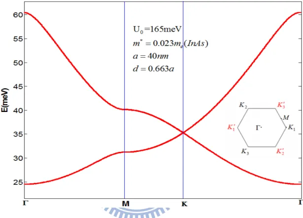
There are the numerical result of energy distribution in MTP lattice (Fig. 2.2), we can see the Dirac point at K point, this phenomenon confirm with the results proposed by Cheol-Hwan Park and Steven G. Louie* [12].
Figure 2.2: The lowest two energy bands calculation of a hexagonal 2DEG superlattice . The Dirac point energy which is at the crossing of the two bands.
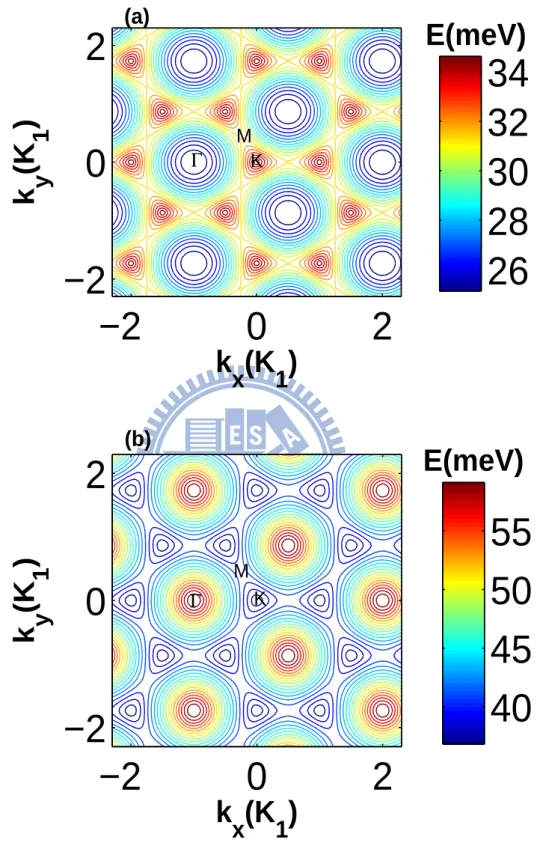
And the Fig. 2.3 shows the results of our rework which are a periodic structure (for wide area in k-space can obviously discover it) and we can see the Dirac points at each corners of Brilloin zone. And the results for other higher energy bands dispersion are showed in appendixC.
CHAPTER 2. ENERGY BAND STRUCTURE WITHOUT SOI EFFECT
k
x
(K
1
)
k
y
(K
1
)
−2
0
2
−2
0
2
k
x
(K
1
)
k
y
(K
1
)
−2
0
2
−2
0
2
40
45
50
55
26
28
30
32
34
(a)
M
K
Γ
E(meV)
(b)
M
K
Γ
E(meV)
Figure 2.3: The contour of energy dispersion for (a) the first lowest band, (b) the second lowest band which m∗ = 0.023m
CHAPTER 2. ENERGY BAND STRUCTURE WITHOUT SOI EFFECT
2.1.1
The Analytical result by perturbation method
The wave function Ψκ(r) can be approximately expressed as a linear superposition (as
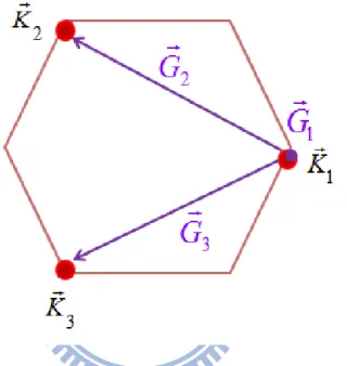
show asEq. (2.2)) of three plane-wave states. The reason for choosing this three basis (K1, K2, K3) is that they are same energy and connected by the most simple reciprocal
vectors G1, G2 and G3 ( shown in Fig. 2.4),
Figure 2.4: This figure shows the wave function which be expanded to K1, K2, K3 by
Gm.
Ψκ(r) = √1
3Ac
[c1exp (i (K1 + k) · r) + c2exp (i (K2+ k) · r) + c3exp (i (K3+ k) · r)] ,
(2.7)
where√1
3Ac is the normalized coefficient of the wave function and K1, K2, and K3represent
wavevectors at the supercell Brillouin zone corners 1, 2, and 3, respectively, in Fig. 2.4. Because of the Schr¨odinger equation HΨ = EΨ and Eq. (3.1), we can obtain those equations as bellow:
CHAPTER 2. ENERGY BAND STRUCTURE WITHOUT SOI EFFECT ei(K1+k)·r n c1 h ~2 2m∗(k + K1+ G1) 2+ V0 1−1 i + c2V01−2+ c3V01−3 o = ei(K1+k)·rE 1c1 ei(K2+k)·r n c1V02−1+ c2 h ~2 2m∗(k + K1+ G2)2 + V02−2 i + c3V02−3 o = ei(K2+k)·rE 2c2 ei(K3+k)·r n c1V03−1+ c2V03−2+ c3 h ~2 2m∗(k + K1+ G3) 2+ V0 3−3 io = ei(K3+k)·rE 3c3 , (2.8) where K1 + G1 = K1, K1+ G2 = K2, K1+ G3 = K3.
Equivalently, we could express the eigenstate as a three-component column vector c = (c1, c2, c3)T . Within this basis, the Hamiltonian H (which ignore the k2 term,
because the secondly contribution can be ignored), will give us
~2K2 2m∗ 1 0 0 0 1 0 0 0 1 + H0+ H1, H0 = W 0 1 1 1 0 1 1 1 0 , (2.9) , where V0 n−m = V01−2 = V02−1 = V01−3 = V03−1 = V02−3 = V03−2=W; V01−1 = V02−2 = V0 3−2= 0 ( V0m = √3G2πUma0d1a2J1(Gm2d)) and H1 = ~υ0k cos θk 0 0 0 cos(θk− 2π3 ) 0 0 0 cos(θk− 4π3 ) , (2.10) where ~2
CHAPTER 2. ENERGY BAND STRUCTURE WITHOUT SOI EFFECT
wavevector k from the +x direction. The eigenvalues of the unperturbed Hamiltonian
H0 are given by E0 = −W, −W, 2W . These two degenerated eigenvectors of H0 with the
same eigenvalue -W. |c1i = 1 √ 2 0 1 −1 , (2.11) |c2i = 1 √ 6 2 −1 −1 . (2.12)
Thus H1 can be treated as a perturbation, which is approximate for ~υ0k < W and
restricted to the sub-Hilbert space spanned by the two vectors is represented by a 2 × 2 matrix ˜H1(degenerate perturbation theory).
˜ H1 = < c1|H1|c1 > < c1|H1|c2 > < c2|H1|c1 > < c2|H1|c2 > = ~υ0 2 −kx −ky −ky kx . (2.13)
The eigenenergies of ˜H1 are given by
E (k) = ±~υ0
2 k. (2.14)
Therefore we can see at k=0, there are degenerate eigenstates and the group velocity near K (k ≈ 0) shows the linear behavior comparing with Fig. 2.2.
CHAPTER 2. ENERGY BAND STRUCTURE WITHOUT SOI EFFECT
2.2
The numerical result compare with single well
system
We use the same program to calculate the case of U0=-300meV. When the extra potential
is negative, the MTP are consisted of many single wells. Such wave under MTP can be illustrated by the overlapping wave function of the nearest single wells.
Schr¨odinger equation in cylinder coordinates, can be written by ½ − ~ 2 2m∗ · 1 r d dr(r d dr) + 1 r2 d dφ2 ¸ + V (r) ¾ Ψ(r, φ) = EΨ(r, φ) . (2.15)
Applying the factored form Ψ(r, φ) = R(r)Φ(φ), where R(r) is the radial part, and φ is the angle between r and ˆx, one can obtain
A R(r) d dr(r dR(r) dr ) − r 2(V (r) − E) = −A d2Φ(φ) Φ(φ)dφ2. (2.16)
This Schr¨odinger can be decoupled into the radial and azimuthal parts,
d2R(r) dr2 + 1 r dR(r) dr + · (V (r) − E) −A − l2 r2 ¸ R(r) = 0, d2Φ(φ) dφ2 = −l 2Φ(φ), (2.17) where we assume A= ~2
2m∗, and the disk-shaped potential V (r) = −V0θ(d2 − r), V0 > 0 is
external potential strength; d is the diameter of potential region.
The solution of radial equation is the Bessel equation. Therefore the electron wave function in two dimensions can be written in form
Ψl(r, φ) = ClJl(αr)eilφ r ≤ d2 , ElKl(βr)eilφ r ≥ d2, where α = q V0+E A ; β = q |E|
CHAPTER 2. ENERGY BAND STRUCTURE WITHOUT SOI EFFECT
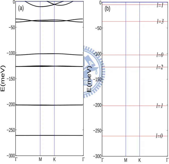
r = d
2, therefore we can get the energy level of finite single well. The Fig. 2.5 shows (a)
MTP case and (b) single well case, where the l is the orbital quantum number, the l=0 is single state; |l|=1 includes two state. Although the single well energy band structure is not exactly as same as muffin-tin potential, the band energy level agrees quite well with each other.
−300
−250
−200
−150
−100
−50
0
E(meV)
−300
−250
−200
−150
−100
−50
0
E(meV)
Γ
M
Γ
M
K
Γ
K
Γ
l=0
l=1
l=3
l=0
l=2
l=1
(a)
(b)
Figure 2.5: The energy band structure for (a) the numerical MTP in 2DEG sys-tem. Compared the energy level with (b) the single well in 2DEG syssys-tem. U0 = −300meV , a = 40nm ; d=0.663a.
CHAPTER 2. ENERGY BAND STRUCTURE WITHOUT SOI EFFECT
2.3
Brief summary
In this chapter, we show that the energy band structures excluding SOI effect in external periodic potential in 2DEG. There are massless Dirac points at the corners of Brilloin zone (K1 points) as graphene system.
And we also do another work for inspecting the numerical results. The wave function be expanded from Γ point and compare the numerical energy dispersion with the results which the wave function be expanded from K1. The result for comparison is exactly the
Chapter 3
Energy band structure with SOI
effect
In this chapter, we consider the effect of spin-orbit coupling on the energy band structure, we have discussed in Chapter 2. The spin-orbit is arisen from the in-plane gradient of the periodic potential.
3.1
Muffin-tin potential lattice in the presence of SOI
The Hamlitonian H for a 2D MTP system with spin-orbital interaction can be expressed by.
H = p2
2m∗ + V (r) + HSO. (3.1)
The spin-orbit interaction term, in vacuum can be desired by
HSO = eλ ~σ ·(p × E) = − eλ ~ σ ·(p × ∇U) = λ ~σ ·(p × ∇V ) = − λ ~σ ·(∇V × p) , (3.2)
where in-plane electric field E = −∇U (U: electric potential); V (Electric potential en-ergy)= - eU (e > 0 ) ; spin-orbit coupling constant λ=120˚A2 (for InAs)
CHAPTER 3. ENERGY BAND STRUCTURE WITH SOI EFFECT
The wave function includes both spin-up and spin-down component in column vector form: Ψκ(r) = eiκ·r X n eiGn·r cn↑ cn↓ . (3.3)
The Hamlitonian of SOI term operates on the wave function leading to:
HSOΨ (r) = −iλ ~ X m eiGm·rV0 mσ · (Gm× p) X n ei(Gn+κ)·r cn↑ cn↓ = −iλ ~ P m eiGm·rV0 m(Gm× p)z 0 0 −P m eiGm·rV0 m(Gm× p)z P n ei(Gn+κ)·rcn↑ P n ei(Gn+κ)·rc n↓ = −iλX mn ei[Gm+(Gn+κ)]·r cn↑V 0 m(Gm× (Gn+ κ))z −cn↓Vm0 (Gm× (Gn+ κ))z , (3.4)
where Gm× p is along z-direction, so σ·ˆz = σzand
P n,m ei(Gm+Gn)·rV0 mcn = P n0,m eiGn0·rV0 mcn0−m = P n,m eiGn·rV0 mcn−m = P n,m0 eiGn·rV0
n−m0cm0( m0 = m). The matrix here is diagonal,
show-ing that spin-up and spin-down are decoupled because HSO depends only on σz. Due
to Eq. (3.1), and Schr¨odinger equation HΨ (r) = EΨ (r), and the orthogonal term of plane-wave form eik·rei(K1+Gn)·rcan be a substrate the m’th component to form a matrix
equation. For getting the simple numerical formulation, we take off eik·rei(K1+Gn)·r and
CHAPTER 3. ENERGY BAND STRUCTURE WITH SOI EFFECT ~2 2m∗ X n k 2+ 2k · (G n+ K1) + (Gn+ K1)2 0 0 k2+ 2k · (G n+ K1) + (Gn+ K1)2 cn↑ cn↓ + X mn V0 n−m 1 − iλ [Gn−m× (Gm+ κ)] 0 0 1 + iλ [Gn−m× (Gm+ κ)] cm↑ cm↓ =X n Ecn↑ Ecn↓ . (3.5)
This equation shows that the spin-up cn↑part is decoupled with spin-down cn↓(the element
only exist on diagonal term). The numerical result is shown on the subsection 3.4. The Fig. 3.5 shows the lowest two bands with wave vector near K1. We can see that
the original Dirac point opens up a gap in the presence of SOI and the numerical result shows Ecn↑ = Ecn↓.
3.1.1
The Analytical result in the presence of SOI by
perturba-tion method
The subsection will show the analytical calculation in our system in the presence of SOI . The Schr¨odinger equation for a 2DEG in the presence of SOI, using the Eq. (3.1) and Eq. (3.2) (where we defined HSO = hSOσz, because of ∇V × p is along z direction) can
be written in the following form
HΨκ(r) = · p2 2m∗ + V (r) ¸ 1 0 0 1 + hSO 1 0 0 −1 e iκ·rX n eiGn·r cn↑ cn↓ = eiκ·rX n eiGn·rEn cn↑ cn↓ . (3.6)
CHAPTER 3. ENERGY BAND STRUCTURE WITH SOI EFFECT
The wave function Ψκ(r)κ = Ψ (r)k+K1 ( k is very close to K1, all at the equivalent
K points (see Fig. 2.4 ) can be approximately expressed as a linear superposition of three plane-wave states,
Ψκ,s(r) =
1
√
3Ac
[c1sexp (i (K1+ k) · r) + c2sexp (i (K2+ k) · r) + c3sexp (i (K3+ k) · r)] ,
(3.7)
where s = ±1 (spin up s=1; spin down s=-1), and 2mp2∗ + V (r) expand is subspace of
|k + K1i, |k + K2i and |k + K3i, will give
~2K2 2m∗ 1 0 0 0 1 0 0 0 1 + H0+ H1,
Here, H0, given by Eq. (2.9), denotes the effect of V (r), and H1 given by Eq. (2.10)
which is linear in k.
The Eq. (3.6) has a spin-orbit term, as show bellow
hSOΨs=±1(r) = −iλeik·rP m V0 m £ ei[K1+(G1+Gm)]·r{G m× [G1+ (K1+ k)]}c1s + e i[K1+(G2+Gm)]·r{G m× [G2+ (K1+ k)]} c2s ei[K1+(G3+Gm)]·r{G m× [G3+ (K1+ k)]} c3s = −iλeik·rP m V0 m £ ei(K1+Gm)·rG m× (K1+ k)c1s + ei(K2+Gm)·rG m× (K2+ k) c2s + e i(K3+Gm)·rG m× (K3+ k) c3s ¤ , (3.8)
CHAPTER 3. ENERGY BAND STRUCTURE WITH SOI EFFECT hSOΨs=±1(r) = −iλ V0 1−1G1−1× (κ1) V01−2G1−2× (κ2) V01−3G1−3× (κ3) V0 2−1G2−1× (κ1) V02−2G2−2× (κ2) V02−3G2−3× (κ3) V0 3−1G3−1× (κ1) V03−2G3−2× (κ2) V03−3G3−3× (κ3) ei(K1+k)·rc 1s ei(K2+k)·rc 2s ei(K3+k)·rc 3s = E1sei(K1+k)·rc1s E2sei(K2+k)·rc2s E3sei(K3+k)·rc3s , (3.9)
where κ1 = K1+k, κ2 = K2+k, κ2 = K2+k, and the same spatial factor eik·rei(Gn+K1)·r
on both side can be ignore for the matrix form.
hSO(κ) = −iλW 0 (G1−2× K2+ G1−2× k) (G1−3× K3+ G1−3× k) (G2−1× K1+ G2−1× k) 0 (G2−3× K3+ G2−3× k) (G3−1× K1+ G3−1× k) (G3−2× K2+ G3−2× k) 0 , (3.10) where V0 n−m = V01−2 = V02−1 = V01−3 = V03−1 = V02−3 = V03−2=W; V01−1 = V0 2−2= V03−2= 0 ( V0m = √3G2πUm0ad 1a2J1( Gmd
2 )), and we also assume A = Gn−m· Knsin(5π6 )
At the K point, the H0 has a doubly degenerate energy -W. Using the correspond
eigen-states, |c1i and |c2i given by, Eq. (2.11), Eq. (2.12), we obtain the 2 × 2 subspace
CHAPTER 3. ENERGY BAND STRUCTURE WITH SOI EFFECT ˜ H0 = hc1| H0|c1i hc1| H0|c2i hc2| H0 |c1i hc2| H0|c2i = −W 1 0 0 1 , (3.11) ˜ H1 = hc1| H1|c1i hc1| H1|c2i hc2| H1|c1i hc2| H1|c2i = ~v0 2 −kx −ky −ky kx , (3.12) ˜hSO,s= hc1| HSO|c1i hc1| HSO|c2i hc2| HSO|c1i hc2| HSO|c2i = i√3sλW A 0 1 −1 0 , (3.13)
where λ is spin-orbit coupling constant. We ignore the energy shift term ˜H0 and
obtain: ˜ H1+ ˜hSO,s= − ~v0 2 kx −~v20ky+ i √ 3sλW A −~v0 2 ky − i √ 3sλW A ~v0 2 kx , (3.14) E = −W ± sµ ~v0 2 k ¶2 + 3 (sAλW )2. (3.15)
The Eq. (3.15) shows the lowest two energy bands at K point opens up a gap (2√3AλW ), the s=1 (spin-up)and s=-1 (spin-down) the energy dispersion is the same ( which is as same as numerical result, see subsection 3.4).
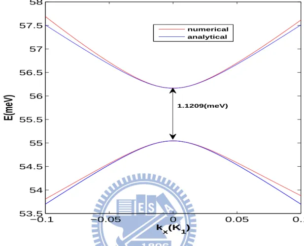
CHAPTER 3. ENERGY BAND STRUCTURE WITH SOI EFFECT −0.1 −0.05 0 0.05 0.1 53.5 54 54.5 55 55.5 56 56.5 57 57.5 58 k x(K1)
E(meV)
numerical analytical 1.1209(meV)Figure 3.1: The lowest two bands which wave vector is near K1 (ky=0, −0.1K1 < kx <
0.1K1). The red line: the numerical result for three K point with SOI; blue line: the
analytic result for 2 × 2 matrix with SOI, λ=120˚A2(InAs); m∗ = 0.023m
e; U0 = 165meV;
a=40nm; d=0.663a.
The Fig. 3.5 shows the energy of analytic energy band (restrict in subspace) is higher than numerical energy band (3 × 3 matrix) except the k ≈ 0 (close to K1). Because of the
numerical energy band consider the 2W (higher energy), leading the energy higher than analytic energy band (only consider -W).
3.2
The position symmetry for muffin-tin triangular
lattice
There are an external muffin-tin triangular potential in the 2DEG. This structure has a symmetry property for rotating 60◦ alone the z-axis. We can interpret the symmetry
CHAPTER 3. ENERGY BAND STRUCTURE WITH SOI EFFECT
property from Fig. 3.2, each muffin-tin triangular structure (a), (b), (c) in real-space have the corresponding BZ (a), (b), (c) in k-space. For example, the figure (a) rotate 60◦ to
becomes figure (b) in real-space and the K system in (a) change to K0 system in (b)
relatively in k-space. Because of the action for rotating 60◦ doesn’t change the structure,
the rotating symmetry is tenable.
Figure 3.2: This figure shows the rotating symmetry property for triangular lattice, the original system (a) in real-space correspond to (a) in k-space, then rotate π
3 from central
point to become (b) in real-space and k-space , and do the same work to become (c) in real-space and k-space, where ˜n is an integer(the blue point note the system which has
been rotated ).
For the analytic calculation, the wave function expanded from K0
1 point(using the K10, K0
CHAPTER 3. ENERGY BAND STRUCTURE WITH SOI EFFECT
from K system which the k become -k.
H1 = −~υ0k cos θk 0 0 0 cos(θk− 2π3 ) 0 0 0 cos(θk− 4π3 ) , (3.16)
Therefore, we obtain the subspace (as show in Eq. (3.12) and Eq. (3.13)) representation of H0, H1 and hSO , and count the energy dispersion. The result of energy dispersion in K0 system is as same as K system E = −W ±q¡~v0
2 k
¢2
+ 3 (sAλW )2. This result prove the position symmetry property( show in Fig. 3.2) which is authentic.
3.3
The numerical result compare with single well
system in the presence of SOI
Using the same numerical program calculates the case of U0=-300meV. When the extra
potential is negative, the MTP resembles many single wells. Such wave under MTP can be illustrated by the overlapping wave functions of the nearest single wells.
HSO = − λ ~σ · µ ˆ r∂V ∂r × p ¶ = − λ ~r ∂V ∂r σ · (r × p) = − λ ~r ∂V ∂r σzLz. (3.17)
The disk-shaped potential with step-like profileV (r) = −V0θ(d2 − r) gives rise to SOI
term, where d is the diameter of the single well.
HSO = − λV0δ ¡d 2 − r ¢ ~r σzLz. (3.18)
The total wave function with spin state χs is written as Ψκ,s(r, φ) = Rsl(r)Φ(φ)χs = Rs
l(r)eilφχs.
CHAPTER 3. ENERGY BAND STRUCTURE WITH SOI EFFECT
wave function into the Schrodinger equation, the radial differential equation reads · d dr(r d dr) − l2 r − rV (r) A − lsHSO A ¸ Rs l(r) = − r AER s l(r). (3.19)
The radial function Rs
l(r) has different coefficients for inside and outside the disk, that
depend on the index s, given by
Rs l(r) = Cs lJl(αr) r ≤ d2 , Es lKl(βr) r ≥ d2, (3.20)
The HSO is nonzero only at r=d2, the boundary condition that bring forth the spin
de-generacy is given by rdRl(r) dr ¯ ¯ ¯ ¯ d 2 + d 2 − + λlsV0 A Rl( d 2) = 0 . (3.21)
Finally,the wave function is continuous at boundary, we obtain the coefficient Cs l , Els
, energy level, and orbital quantum number.
Compared with the energy level of a single well, we can obviously discover the each energy band is almost same level (see Fig. 3.3). There are two energy bands equal to same orbital quantum number(l) when the |l| 6= 0. For the (l)=0 case, only have one energy band because the l=0 did not have opposite quantum number. This work can provide a method to prove the program which is authentic.
CHAPTER 3. ENERGY BAND STRUCTURE WITH SOI EFFECT −300 −250 −200 −150 −100 −50 0 E(meV) −300 −250 −200 −150 −100 −50 0 E(meV) Γ M K Γ Γ M K Γ
l=0
l=1
l=2
l=0
l=3
l=1
Figure 3.3: Energy band structure with parameters units typical for InAs are: effective mass m∗=0.023m
e; a = 40nm; SO coupling constant λ=120˚A2 (a) numerical
muffin-tin potential (U0 = −300meV ) in the presence of SOI. Compared with (b) single well
CHAPTER 3. ENERGY BAND STRUCTURE WITH SOI EFFECT
3.4
Results for energy band structure in the presence
of SOI
In our numerical examples, physic parameters are chosen for InAs in the practical ex-perimental parameters. The Fig. 3.4 shows the energy dispersion with SOI which open
Figure 3.4: Parameters units typical for InAs are: effective mass m∗=0.023m
e; U0 =
165meV , a = 40nm ; SO coupling constant λ=120˚A2 The blue line is without SOI and
the red line is with SOI which spin-up and spin -down are flipping in muffin-tin lattice .
CHAPTER 3. ENERGY BAND STRUCTURE WITH SOI EFFECT
spin-up states and spin-down states are same energy dispersion but spins opposite site in z-direction (Fig. 3.4). And for the lowest two energy band, the spin-up and spin-down
34.5
35
35.5
36
E(meV)
K
Figure 3.5: The lowest two bands which wave vector is near K1. Red circle: the system
with SOI; blue star: the system without SOI, λ=120˚A2(InAs); m∗ = 0.023m
e; U0 =
165meV; a=40nm; d=0.663a.
states mixing at K1 point without SOI (see Eq. (3.5)).
· HSO, p2 2m∗ + V (r) ¸ = · (∂xV ) py− (∂yV ) px, p2 2m∗ + V (r) ¸ 6= 0 . (3.22)
Because of Eq. (3.22), the states at K point is a superposition state with the basis is the eigenstate without SOI, leading to open up a gape for first lowest energy band and second
CHAPTER 3. ENERGY BAND STRUCTURE WITH SOI EFFECT
lowest energy band (Fig. 3.5).
1 2 3 4 5 6 7 8 9 10 11 0.3 0.4 0.5 0.6 0.7 0.8 0.9 1 1.1 Crange gap(meV)
Figure 3.6: This figure shows the value of gap for first lowest energy band and second lowest energy band which depend on Crange(show in appendix A).
The Fig. 3.6 shows the magnitude of the gap ( between first lowest energy band and second lowest energy band) would decrease when the Crange ( orbital index) increase.
We have trying other parameters for different a, d, U0, and roughly discuss the results,
because for Crange=1 ( shown in appendix E).
3.5
The relationship between time reversal property
and our system
The numerical results show the energy dispersion of spin-up and spin-down states are same energy dispersion. We analyze the these results by time reversal symmetry. The wave function and Schr¨odinger equation are given by
CHAPTER 3. ENERGY BAND STRUCTURE WITH SOI EFFECT Ψκ,s(r) = eiκ·r X s uκ,s(r) χs = eiκ·r uκ,s(r) 0 s=1 + 0 uκ,s(r) s=−1 , (3.23) HΨκ,s(r) = H0 1 0 0 1 + hso 1 0 0 −1 e iκ·rX n eiGn·r cn,κ,s=1 cn,κ,s=−1 = eiκ·rX n eiGn·r Es=1cn,κ,s=1 Es=−1cn,κ,s=−1 , (3.24)
where the periodic function ucκ,s=1(r) =
P
n
eiGn·rc
n,κ,s; s = ±1 is meaning spin-up and
spin-down and the definition of HSO = −iλ~
P
m
eiGm·rV0
mσ · (Gm× p) = hsoσz. Because of σzχs= sχs the Schr¨odinger equation turns out to be:
(HN.SO+ shSO) eiκ·r|uκ,si χs = Eκ,seiκ·r|uκ,si χs. (3.25)
Time reversal operator Θ acts on Eq. (3.25), one obtain that
(HN.SO− shSO) e−iκ·r|u−κ,−si χ−s= Eκ,se−iκ·r|u−κ,−si χ−s, (3.26)
where ΘhSO = Θ " −iλ ~ X m eiGm·rV0 m(Gm× p)z # = iλ ~ X m eiGm·rV0 m(G−m× −p)zΘ = −hSOΘ, (3.27) and Θ |uκ,si χs= |uκ,si∗σyχs = |uκ,si∗χ−s eiδ ⇒ |u−κ,−si = |uκ,si∗.
CHAPTER 3. ENERGY BAND STRUCTURE WITH SOI EFFECT
The eigenstate of Eq. (3.26) is |u−κ,−si, so the eigenenergy of this system must be E−κ,−s
which implicate Eκ,s = E−κ,−s, and because Eκ,−s= E−κ,−s, which comes from the parity
operator π acting on Eq. (3.25), we obtain
(HN.SO+ shSO) e−iκ·r|u−κ,si χs = Eκ,se−iκ·r|u−κ,si χs, (3.28)
where the rotating symmetry for triangular lattice (see Fig. 3.2 shows the system in our model with inversion symmetry, the result Eκ,s = Eκ,−s is proven.
3.6
Brief summary
Thus far in this chapter, we show that the energy band structure with SOI effect in external periodic potential in 2DEG. There exist a massless Dirac point at K1 without
SOI effect ( as show in chapert2), and we considered the MTP gradient which arise the SOI, the degenerated energy at K point can open up a gap, and we also have an analytic calculation to prove the numerical result is authentic.
Chapter 4
Berry curvature with SOI effect in
our system
Berry curvature is as a local gauge potential and gauge field associated with the Berry phase. These concepts were introduced by Michael Berry in a paper published in 1984 [14] emphasizing how geometric phases provide a powerful unifying concept in several branches of classical and quantum physics. Such phase have come to be know as Berry phases. In this chapter, we will show the Berry curvature with SOI effect in our system.
4.1
Berry phase
In quantum mechanics, the Berry phase arises in a cyclic adiabatic evolution. The quan-tum adiabatic theorem applies to a system whose Hamiltonian H(κ) depends on κ that varies with time t. If the n’th eigenvalue εn(κ) remains non-degenerate everywhere along
the path and the variation with time t is sufficiently slow, then a system initially in the eigenstate ¯¯uκ(0),n
®
will remain in an instantaneous eigenstate ¯¯uκ(t),n
®
, up to a phase, throughout the process. The state at time t can be written as
|Ψn(t)i = eiγn(t)e− i ~ t R 0 dt0ε n(κ(t0))¯ ¯uκ(t),n ® , (4.1)
CHAPTER 4. BERRY CURVATURE WITH SOI EFFECT IN OUR SYSTEM
where the second exponential term is ”dynamic phase factor” and the first exponential term is the geometric term, with γn being the Berry phase. By plugging into the
time-dependent Schr¨odinger equation, we can obtain the solution of γn(t)
γn(t) = i t Z 0 dt0u κ(t0),n ¯ ¯ d dt0 ¯ ¯uκ(t0),n ® = i κ(t) Z κ(0) dκ · huκ,n| d dκ|uκ,ni . (4.2)
In the case of a cyclic evolution around a close path κ (t) = κ (0), From Stoke’s theorem, we have
γn(C) = i Z Z C dS · ∇κ× huκ,n| ∇κuκ,ni = Z Z C dS · Ωn(κ) , (4.3)
where Ωn(κ) = i∇κ× huκ,n| ∇κuκ,ni is call the Berry curvature. One might worry that
the arbitrary phase attached our expression in Eq. (4.3). To examine this we consider the following gauge transformation |˜uκ,ni = eiξ(κ)|uκ,ni, where the eiξ(κ) is a κ dependent
phase factor. We get huκ,n | ∇κuκ,ni = i∇κξ (κ) + huκ,n| ∇κuκ,ni, and in substituting
into Eq. (4.3), the additional term ∇κ× ∇κξ (κ) = 0. This step shows that the Berry
curvature is independent of arbitrary phase factor which dependent on κ in the wave function. As such, the definition of Berry phase in Eq. (4.3) is uniquely defined.
4.2
Berry curvature analysis
For a closed path C that forms the boundary of a surface S , the closed-path Berry phase can be rewritten using Stokes’ theorem as γn =
R
S
dS · Ωn(κ). From Eq. (4.3), we get:
CHAPTER 4. BERRY CURVATURE WITH SOI EFFECT IN OUR SYSTEM γn(C) = i Z Z C dS · ∇κ× huκ,n| ∇κuκ,ni = i Z Z C dS · [h∇kuκ,n| × |∇κuκ,ni + huκ,n| ∇κ× ∇κuκ,ni] = Z Z C dS · Ωn(κ) . (4.4)
The formulation is as shown below: a complete set P
n0
|∇κuκ,n0i h∇κuκ,n0|=1 has been
inserted in the second row of Eq. (4.4), and they are grouped into n 6= n0 and n = n0
terms. Ωn(κ) = i h∇κuκ,n| × |∇κuκ,ni = i à X n6=n0 h∇kuk,n | uk,n0i × huk,n0 | ∇κuκ,ni + X n=n0 h∇κuκ,n | uκ,n0i × huk,n0 | ∇κuκ,ni ! . (4.5)
Because of ∇κhuκ,n | uκ,ni = 0,
∇κhuκ,n | uκ,ni
= h∇κuκ,n| uκ,ni + huκ,n | ∇κuκ,ni = huκ,n | ∇κuκ,ni∗+ huκ,n | ∇κuκ,ni = 0,
(4.6)
where huκ,n| ∇κuκ,ni must be pure imaginary, as a result of Eq. (4.5) the second term
of the second row is zero.
There is a useful relation for obtaining the numerical formulation:
huκ,n0| (∇κH) |uκ,ni = huκ,n0| (∇kH − H∇κ) |uκ,ni
= huκ,n0| ∇κEκ,n|uκ,ni − huκ,n0| Eκ,n∇κ|uκ,ni
= ∇κEκ,nhuκ,n0 | uκ,ni + Eκ,nhuκ,n0 | ∇κuκ,ni − Eκ,n0huκ,n0 | ∇κuκ,ni
= (Eκ,n− Eκ,n0) huκ,n0 | ∇κuκ,ni ,
CHAPTER 4. BERRY CURVATURE WITH SOI EFFECT IN OUR SYSTEM
where the H (κ) comes from H (κ) = U (κ) HU†(κ) = e−iκ·rHeiκ·r. Because of Schr¨odinger
equation: H |Ψκ,n(r)i = HU†(κ) |uκ,n(r)i = εn(κ) |Ψκ,n(r)i = εn(κ) U†(κ) |uk,n(r)i.
From Eq. (4.7), we obtain:
huκ,n0 | ∇kuκ,ni =
huκ,n0| ∇κH |uκ,ni
Eκ,n− Eκ,n0 , n 6= n
0 , (4.8)
and substituted to Eq. (4.5). The numerical calculation of Berry curvature is read as:
Ωn(κ) = i X n06=n huκ,n| ∂kxH (κ) |uκ,n0i huκ,n0| ∂kyH (κ) |uκ,ni − (x ↔ y) [En0(κ) − En(κ)]2 ˆ z. (4.9)
The Eq. (4.9) shows explicitly, that the Berry curvature is due to the restriction to a single band n and to the resulting virtual transitions to other bands n0 6= n, and the numerical
result n0 is the effective number for two bands which are the nearest for each higher
energy and lower energy (Because of the denominator [En(κ) − En0(κ)]2 in Eq. (4.9)).
For example, the n=1, n0=2, 3 and another case the n=4, n0=2, 3 ( lower energy), 5, 6 (
higher energy).
4.2.1
The analytic result of Berry curvature
The wave function Ψκ,s(r) may be approximately expressed as a linear combination of
three plane-wave states.
The term H1 + HSO, when restricted to the sub-Hilbert space spanned by the two
vectors (the degenerate eigenvectors of lowest two bands) is represented by a 2 × 2 matrix ˜
H1+ ˜HSO (shown in chapter 3.1.1 ), the meaning of this step is that we only focus on the
Berry curvature of k-space near K point(the Dirac point of the lowest band).
˜ H1+ ˜HSO = − ~v0 2 kx −~v20ky+ i √ 3sλW A −~v0 2 ky − i √ 3sλW A ~v0 2 kx , (4.10)
CHAPTER 4. BERRY CURVATURE WITH SOI EFFECT IN OUR SYSTEM −P0kx −P0ky + i∆s −P0ky − i∆s P0kx Yn,s Zn,s = n q (P0k)2+ ∆2s Yn,s Zn,s , (4.11) where ∆s = √
3sλW A, s=±1(spin index) , P0 = ~υ20, υ0 = ~Km∗1; Schr¨odinger equation
h ˜
H1(κ) + ˜HSO(κ)
i
|uκ,n,si = En|uκ,n,si; n = ±1(n = 1, the second lowest band; n = −1,
the first lowest band); Yn,s, Zn,s are the elements of |uκ,n,si. The solution of Eq. (4.11) is Zn,s=
P0kx+n
h√
(P0k)2+∆2s
i
(−P0ky+i∆s) Yn,s and normalize Yn,s, Zn,s (Y
∗ n,sYn,s+ Zn,s∗ Zn,s = 1), we obtain |Yn,s|2 = (P0ky)2 + ∆2s 2 · (P0k)2+ ∆2s+ nP0kx q (P0k)2+ ∆2s ¸. (4.12)
Then we use the above equations, the Eq. (4.9) in this case becomes (the analytic result of Berry curvature)
Ωn=±1(κ) = i (−P0)2 µ Y∗ n,s Zn,s∗ ¶ 1 0 0 −1 Y−n,s Z−n,s µ Y∗ −n,s Z−n,s∗ ¶ 0 1 1 0 Yn,s Zn,s − c.c. 4 (P2 0k2+ ∆2s) ˆ z = i £ P2 0 ¡ Y∗ n,sY−n,s− Zn,s∗ Z−n,s ¢ ¡ Y∗ −n,sZn,s+ Z−n,s∗ Yn,s ¢ − c.c¤ 4 (P2 0k2+ ∆2s) ˆ z = n∆sP 2 0 2£(P0k)2+ ∆2s ¤3 2 ˆ z. (4.13)