Journal of Crystal Growth 192 (1998) 372—375
Very thin layers of TlP grown on InP using gas source
molecular beam epitaxy
Jin-Shung Liu, Jyh-Shyang Wang, Hao-Hsiung Lin*
Department of Electrical Engineering, Room 419, National Taiwan University, Taipei, Taiwan, ROCReceived 16 March 1998
Abstract
Growth of TlP on InP substrates was attempted using gas source molecular beam epitaxy. When the growth temperature is lower than 420°C, Tl3P droplets were found on the InP surface. For higher growth temperatures, a thin accumulation Tl layer in the surface region of the sample was detected by secondary ion mass spectroscopy. By increasing the Tl flux to 8 ML/s at a growth temperature of 450°C, besides the enhancement on the surface density of the Tl layer, an additional peak in the double crystal X-ray rocking curve was found. The 8.5 K photoluminescence spectra are also presented. ( 1998 Elsevier Science B.V. All rights reserved.
PACS: 68.55.Bd; 68.55.Jk; 68.55.Nq
Keywords: Gas source molecular beam epitaxy; III—V compound semiconductors
1. Introduction
Mid- and long-wave infrared detectors and lasers are important optoelectronic devices. Recently, a new infrared material system, InTlP, was pro-posed [1] as an alternative of the dominant InSb and HgCdTe alloys for such applications. The the-oretical calculations predicted that TlP is a semimetal with a band gap of !0.27 eV and therefore, In1~xTlxP spans almost the entire infrared spectrum. Also, it was suggested that In1~xTlxP can be grown in the zinc-blende
* Corresponding author: Fax: #886 2 3632442; e-mail:
structure for all compositions with its lattice con-stant nearly matching that of InP. Few reports have been published regarding the growth of these ma-terials [2—4]. Among them, only Asahi et al. claim-ed the successful growth of TlP and InTlP using gas source molecular beam epitaxy (GSMBE). They reported double crystal X-ray diffraction (DXRD) rocking curves for TlP and InTlP on InP substrates and photoluminescence (PL) spectrum for InTlP with only 1% Tl composition [3,4]. In this study, besides the similar DXRD rocking curves and PL spectra, the results of secondary ion mass spectro-scopy (SIMS) and energy dispersive spectrospectro-scopy (EDS) are reported. When the growth temperature is lower than 420°C, Tl3P droplets were found on the InP surface. For higher growth temperatures, 0022-0248/98/$19.00( 1998 Elsevier Science B.V. All rights reserved.
Fig. 1. The surface morphologies of samples grown at (a) 350°C, (b) 370°C, (c) 385°C, (d) 400°C, and (e) 420°C. a thin Tl accumulation layer in InP, but not in the
TlP layer, was detected by SIMS.
2. Experimental procedure
The growth of TlP on Fe-doped semi-insulating (1 0 0)InP substrates was attempted using VG V80H GSMBE. Elemental Tl and In were used as the group III sources and thermally cracked PH3 was used as the group V source. The amount of Tl input beam flux was estimated from the compari-son with the calibrated In beam flux by the conven-tional beam equivalent pressure (BEP) method, where the different ionization efficiencies for In and Tl in the ion gauge were taken into account. The dependence of Tl vapor pressure on the cell temper-ature is similar to the reported results [2,4].
3. Results and discussion
A set of samples with relatively lower growth temperatures ranging from 350 to 420°C was first attempted. The Tl and PH3 input fluxes were kept at about 1 and 6 ML/s, respectively. After the growth, a 300-A_ -thick InP cap was overgrown at the same growth temperature. The surface mor-phologies of the grown samples are shown in Fig. 1. It can be seen that the surface of sample grown at 420°C is mirror-like but the others contain many large droplets with the density increasing with the decrease of growth temperature. EDS was used to analyze these samples. No Tl signal can be detected for the sample grown at 420°C and for the droplet-free regions of the samples grown below 420°C. Alternatively, the droplet is mainly composed of Tl and P with the Tl/P composition ratio about 3—4 in
Fig. 3. The (4 0 0)DCXD rocking curve of the sample grown at 450°C.
Fig. 2. The surface morphology of the sample grown at 450°C. all samples. These findings show that a growth
temperature of 420°C was high enough to re-evap-orate the incident Tl atoms from the growing sur-face. On the other hand, the lower growth temperature improves the sticking coefficient of Tl. However, instead of two-dimensional growth, the resident Tl adatoms form droplets with P adatoms. The composition is Tl3P, according to the EDS results. This suggests that the formation of a two-dimensional TlP epilayer is not thermodynamically preferable at growth temperatures lower than 420°C.
The second set of samples was grown at relative-ly higher temperatures. The growth temperatures were 420, 435 and 450°C, respectively. For the former two samples, which were grown at 420 and 435°C, respectively, the input Tl and PH3 fluxes were adjusted to 0.5 and 9 ML/s, respective-ly. This very high Tl/P ratio of 18 was an attempt to suppress the Tl desorption. On the other hand, with the same PH3 flux of 9 ML/s, the input Tl flux for the sample grown at 450°C was further in-creased to be as high as 8 ML/s. The use of high input Tl flux was attempted to increase the total amount of Tl incorporation atoms. After the growth, a 0.4-lm-thick InP cap was overgrown at the same growth temperature for each sample in this set.
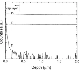
The samples grown at 420 and 435°C have mir-ror-like surfaces and still contain no Tl atoms ac-cording to the EDS results. It indicates that a high Tl/P ratio still cannot effectively prevent the Tl desorption. On the other hand, the surface of the sample grown at 450°C has a high density of tiny droplets and some larger droplets with tails, as shown in Fig. 2. The most remarkable finding is that unlike all the other previous grown samples for which only InP substrate peaks were observed in their DCXD rocking curves, this sample has an additional diffraction peak as can be seen in Fig. 3. The splitting angle between the additional peak and InP peaks is about 105 arcsec. This value is smaller than the reported value of 278 arcsec for TlP by Asahi et al. To further analyze the epilayer, SIMS was employed, and the SIMS profiling is shown in Fig. 4. The striking finding is that the expected TlP epilayer does not exist in this sample. As can be seen, Tl accumulates only in the surface
region and decays very fast in the epilayer. Note that the accumulation layer is in the cap InP layer. Such a profile clearly indicates the surface segrega-tion of Tl during the growth of both the nominal TlP layer and the following InP cap layer. The SIMS profiles of the samples grown at 420 and 435°C also show similar results. However, their surface counts are about one-hundredth of that of the sample grown at 450°C, and are beyond the detectivity of the EDS.
To confirm the finding from SIMS profiling, the 0.3-lm-thick cap layer of the sample grown at 450°C was etched away. The DCXD rocking curve 374 J.-S. Liu et al. / Journal of Crystal Growth 192 (1998) 372–375
Fig. 4. The SIMS profiles of the sample grown at 450°C.
Fig. 5. The 8.5 K PL spectra of the sample grown at 450°C.
of the etched sample was measured again. It was found that the additional diffraction peak dis-appears. The 8.5 K PL spectra for the as-grown and etched samples are shown in Fig. 5. As can be seen, the spectrum for the as-grown sample exhibits a red-shift of about 20 meV compared with that of the etched sample, which is similar to that of undoped InP grown in our system. Clearly, the red-shift results from the incorpo-ration of Tl atoms accumulated in the surface region.
Based on these results, only a low Tl content of InTlP surface layer exists in the sample. Because of no standard sample, our SIMS measurement could not provide absolute Tl content. A rough estima-tion can be made from the EDS measurement that shows the Tl content to be 0.17%. This result was used to convert the integrated SIMS counts ratio between In and Tl within the 1lm spot size of the EDS probe to estimate on absolute concentration. The derived surface Tl mole fraction ratio is about 0.2, which corresponds to a lattice-mismatch be-tween TlP and InP of 0.4%. However, our result is only a rough estimation; further measurements are needed.
4. Conclusions
In summary, a series of samples were attempted for the growth of TlP on InP substrates using GSMBE. When the growth temperature is lower than 420°C, Tl3P droplets were found on the InP surface. For higher growth temperatures, a thin accumulation Tl layer in the surface region of the sample was detected by SIMS. By increasing the Tl flux to 8 ML/s, a thin accumulation Tl layer in the surface region of the sample grown at 450°C was found by using SIMS. DXRD and 8.5 K PL of the layer are presented. A rough estimation suggests that the lattice mismatch between TlP and InP is about 0.4%.
Acknowledgements
This work was supported by the National Science Council, R.O.C. (NSC 87-2215-E-002-010).
References
[1] M.V. Schilfgaarde, A.B. Chen, S. Krishnamurthy, A. Sher, Appl. Phys. Lett. 65 (1994) 2714.
[2] M.J. Anotonell, Mater. Res. Soc. Symp. Proc. (1995) 379.
[3] H. Asahi, K. Yamamoto, K. Iwata, S. Gonda, K. Oc, Jpn. J. Appl. Phys. 35 (1996) L876.
[4] K. Yamamoto, H. Asahi, M. Fushida, K. Iwata, S. Gonda, J. Appl. Phys. 81 (1997) 1704.