薄膜機械特性及殘留應力之反算偵測(3/3)
計畫類別: 個別型計畫 計畫編號: NSC93-2212-E-002-001- 執行期間: 93 年 08 月 01 日至 94 年 07 月 31 日 執行單位: 國立臺灣大學應用力學研究所 計畫主持人: 朱錦洲 報告類型: 完整報告 處理方式: 本計畫可公開查詢中 華 民 國 94 年 10 月 20 日
Contents
Contents ...i
List of Figures...iii
List of Tables...vii
Chapter 1 Introduction ...1
1.1 Motivation ... 1 1.2 Literature Review ... 2 1.3 Research Scope... 4 References ... 5Chapter 2 Metrology Technoques ...8
2.1 Introduction of Phase Measurement ... 9
2.2 Reflection Moire... 12
2.3 Verification ... 15
2.4 Summary... 16
References ... 25
Chapter 3 Mechanical Properties of Sputtered Cu Film ...26
3.1 Mechanical Properties of Si Substrates ... 27
3.2 Analysis Method... 32 3.3 Experimental Procedure ... 35 3.4 Discussions ... 38 References ... 62
Chapter 4 Conclusion ...65
4.1 Conclusion ... 65 4.1.1 Optical Measurement... 65List of Figures
Figure 2.1.1. An illustration of various mechanisms for phase
shifting [1]...17
Figure 2.1.2. Schematic diagram of the relation between the
wrapped and the unwrapped phase [2]. ...18
Figure 2.1.3. Schematic diagram of shadow moiré...19
Figure 2.1.4. Shadow moiré fringes of TSOP with three-step
shifting. (a) The first-step fringe pattern, (b) the second-step fringe
pattern, (c) the third-step fringe pattern...20
Figure 2.1.5. The wrapped phase map of TSOP. ...21
Figure 2.1.6. The unwrapped phase map of TSOP. ...21
Figure 2.1.7. The topography of TSOP reconstructed from the
unwrapped phase. ...22
Figure 2.2.1. Schematic diagram of the experimental setup for
reflection moiré...23
Figure 2.2.2. (a) The deformed grating recorded by the CCD. (b)
The wrapped phase map. (c) The profile of the dashed line in Figure
2(b). (d) The continous distrubution of the phase: unwrapped phase
map...24
Figure 2.2.3. (a) The topography measured from the copper-film
surface with shadow moiré. (b) The wrapped phase map of the
copper-film/silicon sample with reflection moiré. ...25
Figure 3.1.1. The coordinate system of the unit cell of the crystal.
...49
Figure 3.1.2. Orientation of specimens on wafers...50
Figure 3.1.3. Setup of three-point-bending experiment for silicon
substrates...51
Figure 3.1.4. Strain vs. X of the silicon substrate calculated from
Euler Beam equation and FEM using ANSYS...51
Figure 3.1.5. Theoretical elastic moduli vs. orientation on (110)
silicon wafer...52
Figure 3.2.1. Slopes of a layered structure using element Shell99
and element Solid73. ...53
Figure 3.2.2. The fitness history during the searching process of
GA...54
Figure 3.3.1. Schematic diagram of the experimental setup of
reflection moiré for slope change measurement of film-on- substrate
samples...55
Figure 3.3.2. Slope change of 3.7 um sputtered copper film vs.
temperature on Day1 and Day 19. ...56
Figure 3.3.2. Slope change of 4.5 um sputtered copper film vs.
temperature after 2 months. ...56
Figure 3.4.1. Intensity vs. orientation of copper films with
different thickness determined by means of XRD. ...57
Figure 3.4.2. A texture map resulting from grain growth at
temperature
Tggin films of thickness h deposited at
Tdep. The
thermal strain scales with
∆T =Tgg −Tdep[9]...58
Figure 3.4.3. The illustration of structure of sputtered copper
films used in this study. ...59
Figure 3.4.4. Cross section view of 2.2 um thick copper film after
heated at 150°C for 0.5 hrs. ...59
Figure 3.4.5. Schematic cross-sectional views of possible grain
structures of thin films [8]. ...60
Figure 3.4.6(a) Plan-view SEM micrograph of 2.2um thick
copper after heated at 150°C for 0.5 hrs...60
Figure 3.4.6(b) Plan-view SEM micrograph of 3.7um thick
copper after heated at 150°C for 0.5 hrs...61
Figure 3.4.6(c) Plan-view SEM micrograph of 4.5um thick
List of Tables
Table 3.1.1. Theoretical and measured elastic moduli, and the
corresponding deviation for (100) and (110) wafers. ...46
Table 3.2.1. List of given and inversed elastic modulus and CTE,
and the corresponding errors of thin film for verification...47
Table 3.4.1. List of material properties of copper as thin film and
in bulk. ...47
Table 3.4.2. Summary of material properties of copper films in
literatures. ...48
Table 3.4.3. Intensity fraction of microstructures of copper films
with different thickness...48
Chapter 1
Introduction
1.1 Motivation
Flip chip bonding technology boomed because it offers packages a number of possible advantages such as smaller size, higher performance, greater I/O flexibility, and lower cost [1, 2]. Technologies are developed to increase the I/O density and reduce the pitch size of the packages to meet the requirement of smaller packages with higher performance that can sustain an extremely high temperature even under normal operating conditions. Mechanical issues become more responsible for the failure of packages. The coefficient of thermal expansion (CTE) mismatch between the chip and the carrier induces high thermal and mechanical stresses and strain, which eventually cause failure of packages. The reliability of flip chip packaging is partly dominated by the contact bumps. Numerical simulation such as finite element methods has been
employed in structure designs and analysis to predict and optimize the reliability of IC packages. Only if the inputs of material properties are correct, can the outcome be referable to its applications. Under bump metallization (UBM), which usually have thickness of thin-film order, are important parts in a contact bump. However, there are rare studies about the material properties of UBM.
Thin-film materials have been widely used in many applications. The mechanical properties of thin films may be markedly distinct with different processes and processing conditions, but usually difficult to obtain because the thickness of a few micrometers. Therefore, our goal is to develop a method to obtain the mechanical properties of materials with thickness of thin-film order. In this study, copper films are employed due to the emergence as an important material in IC packages in the last few years, which have higher electrical and thermal conductivity, and better resistance to electromigration than aluminum. In addition, the advent of copper-based chip interconnection metallurgy is expected to boost the flip chip technology. It will be possible to directly bond the copper pads with conductive adhesives. This simple processing ability would have a great impact on cost and infrastructure issues by possibly eliminating UBM and maybe the bumping step [3], if the high resistance problem is solved.
1.2 Literature Review
applications. The principal function of thin film components is generally not structural; therefore, the mechanical behavior may not be the major concern for material selection or design [4]. However, it is essential to acquire the knowledge of mechanical properties and responses of thin films such as the Young’s modulus, the coefficient of thermal expansion (CTE), and the stress, which usually dominate the stability and reliability of the devices.
The mechanical properties of thin films may be markedly dependent on the deposited condition, thickness, and the exposed environment. One category of the geometrical configuration for measuring mechanical properties of thin films is freestanding, such as the tensile test [5] and the bulge test [6], which can provide the stress-strain curve. Although measurements on freestanding films are straightforward to derive the intrinsic film properties, the samples require beforehand preparation and fabrication, and the geometrical definition of the film is more difficult. The other category is films on substrates, and the mechanical properties of silicon substrates need to be known in practice. X-ray diffraction is another tool to obtain Young’s modulus of the thin film [7]. Nevertheless, the use is restricted to crystalline thin films, and cost and safety issues are also of concern. Nanoindentor instrument is another popular tool [8], but it is also a destructive method. Literatures for CTE of thin films are very limited. For most foregoing methods, mechanical loading were applied, which didn’t deal with the CTE measurement in general. Radius-of-curvature
measurement with thermal load is adopted. By pairing a substrate with a single CTE with a substrate with anisotropic CTEs, such as Y-cut quartz, Ho et al obtained elastic modulus, Poisson ratio, and CTE of the films [9]. However, single value of each curvature has less resistance to errors, which might be caused from the measuring system such as small deviation of the position when scanning a laser beam over the sample, and the deviation of materials properties of substrates and might influence the result.
As for techniques of optical measurements, to quantify the interfering fringe patterns and to improve the resolution, phase stepping, phase unwrapping and image processing techniques were required and developed [10, 11]. Asundi used the computer generated logical moiré to both static and dynamic applications [12]. Chiang measured the stress in thin films by rotating the grating 90 degrees to form slope fringe patterns in the other orthogonal direction [13]. Yang adopted phase shifting of a cross grating for reflection moiré to simultaneously obtain the slopes of both directions [14]. However, rotating or shifting the grating might not be suitable for the real-time measurement under temperature change.
1.3 Research Scope
In this study, we have developed methods for determining mechanical properties of materials, which include anisotropic silicon wafers and sputtered
thin copper films on silicon substrates. The corresponsive results and phenomena are also discussed.
In Chapter 2, optical measurement techniques are mentioned. Two moiré methods, shadow moiré and reflection moiré, were adopted in this study. The techniques of phase extraction for the optical measurement are briefly introduced first. The implementation of the redeveloped reflection moiré and the verification are then illustrated. Finally, distinctive features of these two optical measurement techniques are summarized.
In Chapter 3, we present a method for obtaining mechanical properties of copper films on silicon substrates. The mechanical properties of silicon substrates are measured first in Section 3.1. The genetic algorithm (GA) with finite element analyses using ANSYS was used to optimally obtain the mechanical parameters of copper films such as elastic modulus and CTE. The analysis method is presented in Section 3.2, and Section 3.3 describes the sample preparation and the procedure of optical measurement. Finally, the results obtained are discussed with further examination in Section 3.4.
In Chapter 4, the conclusions of each topic are narrated respectively, which include the optical measurement and sputtered copper thin films.
References
1. G. A. Riley, “ Introduction to Flip Chip: What, Why, How,” FlipChips.com, 2000. http://www.flipchips.com/tutorial01.html
2. Flip Chip Packaging Technology Solution. http://www.amkor.com
3. K. Gilleo, “The coming of copper UBM,” 2002.
http://www.flipchips.com/tutorial26.html
4. L. B. Freund and S. Suresh, Thin Film Materials: Stress, Defect Formation and Surface Evolution, Cambridge University Press, 2003.
5. D. T. Read, “Young’s Modulus of Thin Films by Speckle Interferometry,” Meas. Sci. Technol., Vol. 9, pp. 676-685, 1998.
6. Y. Xiang, X. Chen and J. J. Vlassak, “The Mechanical Properties of Electroplated Cu Thin Films Measured by Means of the Bulge Test Technique,” Mat. Res. Soc. Symp. Proc., Vol. 695, pp. L4.9.1-L4.9.6, 2002. 7. M. Chinmulgund, R. B. Inturi, and J. A. Barnard, “Effect of Ar Gas Pressure
on Growth, Structure, and Mechanical Properties of Sputtered Ti, Al, TiAl, and Ti3Al Films,” Thin Solid Films, Vol. 270, pp. 260-263, 1995.
8. M. A. EI Khakani, M. Chaker, M. E. O’Hern, and W. C. Oliver, “Linear Dependence of Both the Hardness and the Elastic Modulus of Pulsed Laser Deposited a-SiC Films upon Their Si-C Bond Density,” J. Appl. Phys., Vol. 82, No. 9, pp. 4310-4318, 1997.
9. J. H. Zhao, Y. Du, M. Morgen, and P. S. Ho, “Simultaneous Measurement of Young’s Modulus, Poisson Ratio, and Coefficient of Thermal expansion of Thin Films on Substrates,” J. Appl. Phys., Vol. 87, No. 3, pp. 1575-1577, 2000.
10. K. Creath, “Phase-measurement Interferometry Techniques,” Progress in Optics Vol. XXVI, pp. 351-393, 1998.
11. I. Tsai, C. Z. Tsai, E. Wu, and C. A. Shao, “On Accurate Measurement of Warpage for Electronic Packages,” Proceedings of IMAPS Taiwan Technique
Symposium, pp. 290-297, 2001.
12. Asundi, “Novel Techniques in Reflection Moiré,” Experimental Mechanics, September, pp. 230-242, 1994.
13. F. P. Chiang, “A Whole-field Method for the Measurement of Two-dimensional State of Stress in Thin Films,” Experimental Mechanics, August, pp. 377-380, 1972.
14. J. D. Yang, “Identification of Thin-Film Mechanical Properties by Inverse Methods,” Ph D Dissertation, Institute of Applied Mechanics, National Taiwan University, Taipei, Taiwan, ROC, 2002.
Chapter 2
Metrology Techniques
Optical measurement techniques have been developed widely in various areas owing to their properties of non-contact, whole field, and high accuracy. Two moiré methods, shadow moiré and reflection moiré, were adopted in this study. Shadow moiré is a well-established optical technique for measurement of the out-of-plane displacement, and reflection moiré is used for the partial derivative (slope) of the out-of-plane displacement, in the principal direction of the grating. In Section 2.1, the techniques of phase extraction required for the optical measurement are briefly introduced. The implementation of the redeveloped reflection moiré is illustrated in Section 2.2, and verification is presented in Section 2.3. Distinctive features of these two optical measurement techniques are then summarized in Section 2.4.
2.1 Introduction of Phase Measurement
Fringes are generally the most primitive data recorded with optical measurement methods. The decisive factors in bringing the performance to the limit are automatic quantification of the recorded data and improvement of the resolution. Phase measurement, the theories for which were formed in the 1970s, is the quantitative technique for improving measuring resolution. With the improvement of computers and image recording systems, phase measurement became a more attainable and applicable method for enhancing the measuring precision in the 1980s.
The physical information we seek is usually implied by the intensity of the fringes. The intensity recorded is usually formulated as
( ) ( ) ( )
x y a x y b x y[
( )
x y]
I , = , + , cosφ , (2-1)
where the phase φ
( )
x,y is proportional to the desired information with some factor which relates to the optical setup, a ,( )
x y is the background intensity, and b ,( )
x y is the fringe modulation intensity. There are two categories of methods used to extract the phase from the intensity distribution. One category is image transformation, which usually requires only one image. However, transformation requires complicated calculations and human judgment. The other category, which includes phase shifting or phase stepping methods, is adopted in this study. From Equation (2-1), we can see that there are three unknowns: a ,( )
x y , b ,( )
x y , and φ( )
x,y in a fringe pattern. Therefore, at leastthree fringe images are needed to solve all the unknowns. Phase shifting methods compute the phase through the recording of multiple fringe images. The intensity, with phase shifting, can be expressed as,
( ) ( ) ( )
[
( )
]
(
)
n k k y x y x b y x a y x I r k k k , . 2 , 1 1 , cos , , , K = − = + + = α α α φ (2-2) where I is the intensity distribution of the k k step, th αk is the accumulative increment shifted of the phase for the k step, and th αr is a constant as the step size of each step. Phase shifting, an intention to introduce a modulation to the phase, can be accomplished with various shifting mechanisms, depending on the optical methods used, such as tilting a glass plate, rotating a half-wave plate, moving a mirror for different interferometry, or shifting a grating for moiré methods, as shown in Figure 2.1.1 [1]. The formulas adopted to calculate the phase depends on both the number of steps and the step size. For example, for four steps with a π 2 shift, the phase can be obtained by( )
− − = − 3 1 2 4 1 tan , I I I I y x φ (2-3)For three steps with a 2π 3 shift, the phase can be obtained by
( )
3 2 2 3 tan , 3 1 2 3 1 1 π φ + − − − = − I I I I I y x (2-4)The phase φ
( )
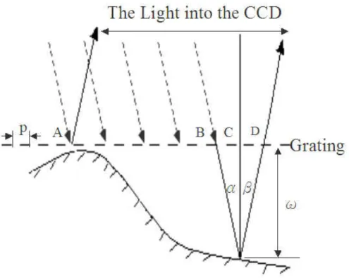
x,y is wrapped in −π ~π because of the trigonometric function employed, and is thus called the wrapped phase map. Phaseunwrapping is then performed to unwrap the −π ~π phase to a continuous phase map, which is related to the desired information. The schematic concept of unwrapping is illustrated in Figure 2.1.2 [2]. Next, we will illustrate the process of quantifying a fringe pattern from shadow moiré with phase shifting techniques mentioned above. The Schematic diagram of shadow moiré is illustrated in Figure 2.1.3. The relation between the phase and the out-of-displacement is as follows:
( )
( )
( ) ( )
π φ β α 2 , , , tan tan , , y x y x N p y x N y x w = + = (2-5)where N is the order of the interfering fringe, p is the grating pitch, α is the angle between the light source and the normal to the grating surface, β is the angle between the CCD and the normal to the grating surface, and φ
( )
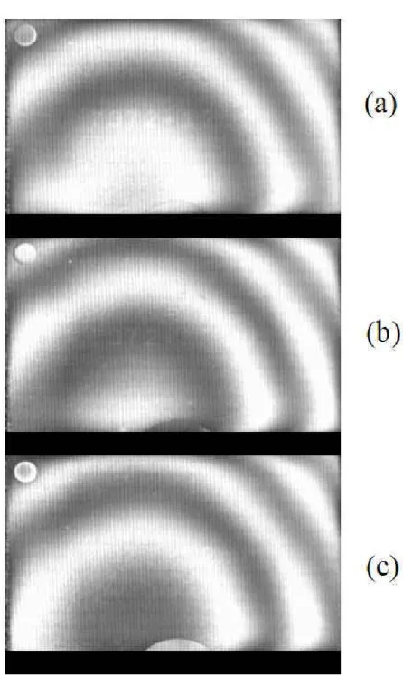
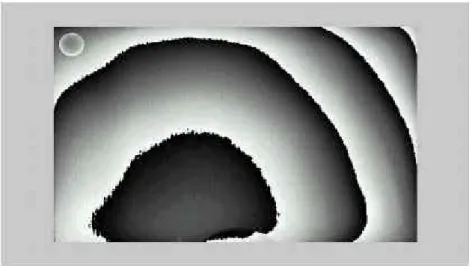
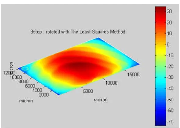
x,y is the unwrapped phase. The package used as the sample here is a TSOP. We make p=100 um, α =45° and β=0° in this application, which make a fringe equal a displacement of 100 um. Three-step phase shifting is adopted here, and each fringe pattern is recorded after a 2π shift, as shown in Figure 2.1.4. Intensity 3 distributions of these three images are substituted into Equation (2-4). The wrapped phase is then obtained by the calculation and shown in Figure 2.1.5. After employing the unwrapping algorithm, the unwrapped phase is obtained and shown in Figure 2.1.6. Through Equation (2-5), the out-of-plan displacement can be related to the unwrapped phase, and the topography of thesample can be obtained, as shown in Figure 2.1.7. In general, phase measurement can improve the accuracy from ten to one hundred times that of fringe intensity.
2.2 Reflection Moire
Numerical differentiation is known as an inaccurate process, and as such should be avoided if possible. In this regard, reflection moiré with slope as the prime experimental data is superior to displacement generating methods, such as shadow moiré and holography. The essentiality of the reflecting sample surface was regarded as the major limitation in its application. Nevertheless, it is favorable for our applications to shiny metallic IMCs and mirror-like surfaces, such as silicon substrates.
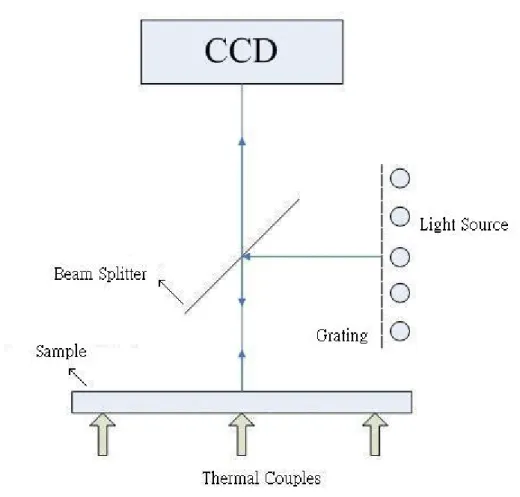
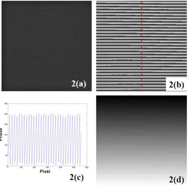
The key points in this section are focused on the implementation of the redeveloped reflection moiré. A schematic diagram of the experimental setup is shown in Figure 2.2.1. The sample used to demonstrate the measurement procedure is a 2.5 cm x 2.5 cm x 350 um (100) silicon substrate with a 2-um copper film deposited on the bottom surface. A white light was passed through the grating and the beam splitter and then reflected from the surface of the sample. The deformed grating was the reflection of the cross grating and recorded with a CCD, as shown in Figure 2.2.2(a). A cross grating was employed to measure the slope change of the two orthogonal directions. To
separate out the information of one direction, the grating of the second direction had to be removed. A 1-by-5 convolution kernel was used as an averaging filter [3], and the dimension of the kernel was determined by the number of pixels of one grating pitch recorded. The intensity of the filtered frame can be written as,
( ) ( ) ( )
x,y a x,y b x,y cos[
2 f0x( )
x,y]
,Ii = + π +φi (2-6)
where the phase φi
( )
x,y contains the desired information, a ,( )
x y is the background intensity, b ,( )
x y is the fringe modulation intensity, and f is the 0spatial-carrier frequency. To extract the phase from the intensity distribution, phase shifting was needed, and this was accomplished by numerically shifting a computer generated grating instead of using an optically shifting mechanism. Any step length can be achieved with numerical shifting, and we chose the Carré four-step formula with a π /2 shift, which is more stable and can cancel out nonlinear terms automatically [1]. The extracted term
[
2πf0x+φi( )
x,y]
can be shown as the wrapped phase map in Figure 2.2.2(b), and the profile of the dashed line is shown in Figure 2.2.2(c). After the wrapped phase was unwrapped, a continuous distribution of the phase could be obtained, as shown in Figure 2.2.2(d). If the sample was undergoing a temperature change, we could record the deformed grating at any temperature. With the same abovementioned procedure, another unwrapped phase[
2πf0x+φf( )
x,y]
can also be obtained. The phase of the slope under any temperature change: ∆φ =(
φf −φi)
, can be obtained by subtracting these two phase maps. The phase related to theexperimental setup is as follows: , 2L Np = ∆θ π φ 2 ∆ = N (2-7)
where ∆θ is the slope change, N is the order of the interfering fringe, p is the grating pitch, and L is the distance from the grating to the sample surface. With p=400 um and L=0.69 m in our case, the resolution is 2.9×10⁻⁴ rad/fringe.
Furthermore, the resolution can be enhanced to the order of 10−6 rad/pixel with
the phase shifting techniques mentioned above, which can be equivalently converted to a resolution of 0.2 um for warpage in a 2.5cm X 2.5cm area.
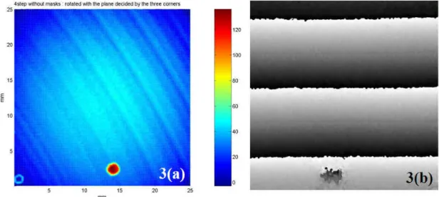
In addition to the extremely high resolution with a relatively coarse grating pitch needed, reflection moiré has the capability of visualizing the sample condition, which is usually not accessible with laser scanning measurement. An example of a bilayer structure, a 2 um copper film deposited on a silicon substrate, is illustrated in Figure 2.2.3. Partial delamination of the copper film caused a small bulge on the copper surface. The topography of the copper-film surface with the small bulge on it could be measured with shadow moiré, as shown in Figure 2.2.3(a). When we turned over the specimen and measured the silicon surface on the other side with reflection moiré, this high-resolution and whole-field measurement allowed the delamination to reveal even the bulge on the copper side, as shown in Figure 2.2.3(b).
2.3 Verification
Owing to the requirement of a mirror-like surface for the employment of reflection moiré, the verification was performed using a slender silicon substrate. The silicon was simply supported and loads of 150g, 175g, and 220g were then applied in turn at the middle of the span. The dimensions of the silicon were 80.0mm in length, 21.0mm in width, and 541.0um in thickness. From the responses of two strain gauges, the Young’s modulus of the silicon in the longitudinal direction was measured to be 165.5 GPa.
Reflection moiré was then applied to measure the slope change in the silicon with loading of 37g at the middle of the span. The CCD recorded the images of the grating from the silicon surface before and after the force was applied. The loading could not be excessively large; otherwise, the deflection would be too large for the deformed surface to stay in focus under this condition. With a grating pitch of p=600.0 um and L= 66.75 cm, the resolution is 4.5×10⁻⁴
rad/fringe, as per Equation (2-7). After the processing procedure described in Section 2.2, the phase change, ∆φ =
(
φf −φi)
, could be obtained by subtracting the loading and unloading phase maps. The slope change was measured to be3
10 57 .
2 × − rad, and the calculated slope change was 2.54×10⁻³rad. From the
results, we can see that the difference of the implementation of the reflection moiré with artificial cross grating developed here was small, only 1.2 %.
2.4 Summary
In this study, two moiré techniques, namely reflection moiré and shadow moiré, were developed to measure the deformation of layered composite structures subjected to thermal loading. An artificial cross grating was also developed for reflection moiré in order to overcome the problems of measurement under temperature change, while at the same time preserving the improved resolution and the two orthogonal slopes.
The techniques developed to quantify fringe patterns and to improve the resolution for reflection moiré include phase stepping, phase unwrapping, and image processing, and these can also be applied to shadow moiré, as has been described previously in detail elsewhere [4]. It is notable for shadow moiré that, for general application, it uses a grating pitch finer than 100 um to reach the resolution of 10 um. However, reflection moiré can bear a relatively coarse grating pitch, such as 400 um, to equivalently obtain the resolution of 0.2 um for warpage, which also efficiently lowers the cost of grating fabrication.
Figure 2.1.2. Schematic diagram of the relation between the wrapped and the unwrapped phase [2].
Figure 2.1.4. Shadow moiré fringes of TSOP with three-step shifting. (a) The first-step fringe pattern, (b) the second-step fringe pattern, (c) the third-step fringe pattern.
Figure 2.1.5. The wrapped phase map of TSOP.
Figure 2.1.7. The topography of TSOP reconstructed from the unwrapped phase.
Figure 2.2.1. Schematic diagram of the experimental setup for reflection moiré.
Figure 2.2.2. (a) The deformed grating recorded by the CCD. (b) The
wrapped phase map. (c) The profile of the dashed line in Figure 2(b). (d) The continous distrubution of the phase: unwrapped phase map.
Figure 2.2.3. (a) The topography measured from the copper-film surface with shadow moiré. (b) The wrapped phase map of the
copper-film/silicon sample with reflection moiré.
References
1. K. Creath, “Phase-measurement interferometry techniques,” Progress in Optics Vol. XXVI, pp. 351-393, 1998.
2. D. C. Ghiglia and M.D. Pritt, Two-dimensional Phase Unwrapping, 1998. 3. Image Processing Toolbox User’s Guide, The MathWorks, Inc., 1997.
4. I. Tsai, C. Z. Tsai, E. Wu, and C. A. Shao, “On Accurate Measurement of Warpage for Electronic Packages,” Proceedings of IMAPS Taiwan
Chapter 3
Mechanical Properties of Sputtered Cu Film
Thin films have been widely used in various technological applications. Though the principal function of thin film components is generally not structural, it is essential to acquire the knowledge of mechanical properties and responses of thin films, which usually dominate the stability and reliability of the devices.
For most methods, mechanical loading was applied, which didn’t deal with the CTE measurement in general. In this chapter, we present a method for obtaining mechanical properties of copper films on silicon substrates. The mechanical properties of silicon substrates also need to be known in practice, which are illustrated in Section 3.1 first. Finite element analyses with ANSYS were then performed, and the genetic algorithm (GA) was used to optimally obtain the mechanical parameters of copper films such as elastic modulus and CTE. The analysis method is presented in Section 3.2 to show how the
numerical algorithm works, and Section 3.3 describes the procedure of optical measurement in progress and the sample preparation. Reflection moiré developed in Chapter2 is adopted here for the mirror-like surface of silicon substrates. Finally, in Section 3.4, the results obtained are discussed with further examination.
3.1 Mechanical Properties of Si Substrates
To study the mechanical behavior of thin films, thin films on substrates are adopted most often. The most commonly used material for substrate is silicon, which has low CTE and is a prevalent semiconductor material. The theoretical values of elastic moduli of silicon were usually applied. However, the values might be different in practice. Before further study of thin-films, the actual mechanical properties of silicon substrates should be cautiously investigated first.
Silicon belongs to the cubic crystal class. In the original crystallographic orientation, there are three independent constants in elastic stiffness of silicon, which are C11=165.6 GPa, C12=63.9GPa, and C44=79.5 GPa [1]. For crystals
with cubic symmetry, the axes of the coordinate system are generally aligned with the edges of the unit cell of the crystal, as shown in Figure 3.1.1. The elastic constants in other coordinate systems are obtained using tensor transformations:
, mnpq ql pk nj mi ijkl a a a a s s′ = (3-1a) , mnpq ql pk nj mi ijkl a a a a c c′ = (3-1b)
where s′ijkl and c′ijkl are the compliance and stiffness tensors in the new coordinate system, and aij is the direction cosine in terms of the Eulerian angles of the crystal coordinate system with respect to the new coordinate system. The transformation law (3-1b) is for Cijkl, a fourth rank tensor. It requires tedious computation, and is not convenient for the 6x6 matrix Cαβ [2].
We introduce the simplified transformation for Cαβ. The 6x6 matrix Cαβ for
cubic materials can be written as follows,
= 44 44 44 11 12 12 12 11 12 12 12 11 0 0 0 0 0 0 0 0 0 0 0 0 0 0 0 0 0 0 0 0 0 0 0 0 c c c c c c c c c c c c C (3-2)
The compliance sαβ can be expressed analogously. The special case of the
transformation is the rotation about the z-axis through an angle θ , and the transformation laws are easily shown as:
,
T KCK
C′= s′=
( )
K−1 TsK−1, (3-3a) − − − − = 2 2 2 2 2 2 0 0 0 0 0 0 0 0 0 0 0 0 0 0 1 0 0 2 0 0 0 2 0 0 0 n m mn mn m n n m mn m n mn n m K − − − − = − 2 2 2 2 2 2 1 0 0 0 0 0 0 0 0 0 0 0 0 0 0 1 0 0 2 0 0 0 2 0 0 0 n m mn mn m n n m mn m n mn n m K (3-3b) where θ cos = m , n=sinθ.
After transferring the matrixes C and s to the new coordination, the elastic modulus (E) in the new coordinate system is then defined by [2]:
(
)(
)
11 12 11 12 11 12 11 2 1 s c c c c c c E ′ = ′ + ′ ′ + ′ ′ − ′ = (3-4)After the transformation conforming to the geometric orientation of (100) wafers with
4
π
θ = , the in-plane elastic moduli of (100) wafers calculated are E<100> = 130.0 GPa, E<110> = E<-110> = 168.9 Gpa following the process
mentioned above. To measure the elastic moduli of silicon substrates, (100) and (110) silicon wafers with both side polished were adopted. The different orientations of specimens cut form (100) and (110) wafers are shown in Figure
3.1.2. Each specimen was cut into 6.0 cm x 1.5 cm. Three slices of (100) wafers with different thickness were used, which were 255 um, 350 um, and 525 um. An ANSYS finite element model was used to examine whether the Euler beam equation is suitable for such specification with anisotropic material properties. The silicon was simply supported and load was applied at the middle of the span as shown in Figure 3.1.3. Euler beam was chosen because it relate strains to the elastic modulus with a very simple equation as:
( )
z Ebh px z x, = 6 2 ε (3-5)where p is the loading force, b and h are the width and height of the beam, and E is the elastic modulus along the longitudinal direction. The strains calculated from 3D FEM using ANSYS were compared with the strain calculated from Euler beam equation in Figure 3.1.4. We can see that near the location where the load and boundaries applied, the strains from Euler beam equation deviated a little from that from FEM because of stress concentration. Therefore, we choose to locate the strain gages at the middle of the load force and each support where the strains from beam equation fit that from FEM well. The result shows that with proper strain gage locations, the in-plane elastic moduli could be successfully obtained with general Euler beam equation (3-5), which were E<100>= 103.6 GPa, E<110>=140.7 GPa, E<-110>= 140.5 Gpa for the 255-um thick
wafer. The measurement agreed with the trend of theoretical values in each orientation. The results of <110> and <-110> directions only had 0.2%
difference. All the experimental data are listed in Table 3.1.1. The percentage of difference for each specimen cut from the same wafer was consistent to each other. The average difference increased from 7.2 % to 17.9 % with the thickness decreasing from 525 um to 255 um. The effect of defects became more obvious in thinner thickness of silicon wafer, and made the elastic moduli smaller than the theoretical values.
On the other hand, the theoretical elastics moduli of (110) wafers repeat every π rad., which is shown in Figure 3.1.5. The in-plane elastic moduli of (110) wafer were determined to be E<-111>= 170.1 GPa, E<1-12>=157.9 GPa with the
same method, which were also smaller but close to the theoretical values with the consistent percentage. The theoretical and measured data of (110) wafers are also listed in Table 3.1.1. Use of the anisotropic (110) wafer aims to make characterization of material properties of the deposited thin film successful because it has different curvatures in each orthogonal directions which can offer more information to determine the thin film material properties.
The applications with thin silicon substrates are gradually increasing. For example, 3D system integration with thin silicon substrates can overcome the performance bottleneck for next IC generation. According to the results above, besides the thin thickness causes the specimens more flexible, the effect of defects in thinner substrates also causes the elastic moduli more deficient, which makes the substrate even more flexible. Therefore, use of thinner wafers always
comes with larger deformation, which might cause other integration problems and should be handled with more consideration.
3.2 Analysis Method
Finite element analyses adopted to calculate the deformation of the film-on-substrate composite structure under thermal loading were performed with ANSYS. A composite element, Shell99 in ANSYS, was introduced because the films on the substrates were of the micrometer order and the selected (100) and (110) silicon substrates were 355 um and 306 um thick respectively. Shell99 that takes the stiffness change along the thickness direction into consideration based on the composite theory is an ideal element for thin film analysis such as our cases here. The results with Shell99 used have been proved to be the same as those with Solid73, an 8-node solid element in ANSYS, as shown in Figure 3.2.1. The model is a 2um thick film on a 250 um thick substrate under temperature change. The slopes from models using these two elements fit well, except for a deviation near the edge, which is because of the unavoidable singularity near the boundary, even using finer mesh. Therefore, when we select data as the input for the searching algorithm, we should leave out the peripheral area, also, the reflection image of which is often affected by chipping effect. The number of the element needed with Shell99 was several times smaller than that with Solid73. In this way, the excessive aspect ratio issues, which were usually
encountered in the thin film analyses, could be avoided. Computation time could also be appreciably saved.
Each case was begun with randomly generating sets of mechanical parameters. ANSYS was employed to calculate the slope of warpage under temperature change. The stiffness matrix of the film-on-substrate composite structure was generated according to the guessed mechanical parameters. The following quadratic objective function was used to find the degree of deviation between the calculated and measured warpage slopes:
∑
= − + − − = N i yi yi cal yi xi xi cal xi fit 1 2 exp exp 2 exp exp φ φ φ φ φ φ (3-6) where cal xi φ and cal yiφ are the calculated slope values in each iteration using the guessed mechanical parameters, exp
xi
φ and exp
yi
φ are the measured slope distributions, and N is the number of the measured data. The reason why the normalized form of the objective function is adopted is that we hope to make each measured point have the equal contribution to the fitness. Through the whole field optical method, we can obtain the points spreading all over the surface, which often have substantially different magnitude. We do not want the searching process to be dominated by some points with large magnitude only, so we choose to normalize the difference first. The ultimate goal was to reduce the deviation between the calculated and measured warpage slopes to its minimal value, and the minus sign was inserted in Equation (3-6) so that the objective
function can be fit to the algorithm set for searching maximum fitness. The genetic algorithm (GA) was adopted as the searching tool. Two mechanical constants, i.e., elastic modulus and coefficient of thermal expansion were then regenerated by GA and the loop repeated until a convergence criterion was satisfied. Use of the genetic algorithm assured convergence of the objective function to a globally maximum value, which was the critical part of this study as there were usually other local extreme values. A detailed description of the solution schemes for the inverse problem can be referred to [3, 4].
Verification of this searching algorithm was performed in imitation of the measurement for copper films on substrates. The specification used in the model is 2.5 cm squared for 350 um-thick (100) silicon substrate and 300 um-thick (110) silicon substrate with 3.7um-thick copper films on each top surface. Use of the anisotropic (110) wafer aims to offer more independent relations for determining the thin film material properties because its anisotropy resulted in different curvatures in each orthogonal directions. A noise of S/N ratio 10 was added to the slope of warpage under temperature change, which was calculated using ANSYS, to cover for the measured slope distributions, exp
xi
φ and exp
yi
φ , in Equation (3-6). Three mechanical parameters of thin films needed for the stiffness matrix of the finite element models are elastic modulus, CTE, and Poisson ratio, which are set as 96.6 Gpa, 38.8 ppm, and 0.19 respectively in this verification. The difficulty of GA in searching out the optimal solution is raised
with increasing number of variables. Since Poisson ratio is intrinsically less sensitive to the deformation than the other two parameters under such configuration, and has the clear and definite range in physics from –1 to 0.5, the value of Poisson ratio is man-made given with the increasing interval of 0.1 in each run with GA. With such certain noise, 9600 data points are needed to robustly obtain the result with Equation (3-6). Such a large amount of data can only be achieved easily with whole-field optical measurements as mentioned in Chapter 2. Best fitness was achieved with Poisson ratio from 0.19 to 0.2, and the optimally obtained elastic modulus is 95.1 GPa, and CTE is 39.1 ppm in average for thin film. We set the generation number as 250. If the best fitness happened at some generation, which is smaller than 20% away from the generation number we set, it is considered not stably converged yet. Then we will increase the generation number next time. With the condition in this case, the fitness converged at the 73rd generation as shown in Figure 3.2.2. The error is less than 2% for both elastic modulus and CTE, and the range of Poisson ratio also fits to the specified value that indicate the algorithm developed is stable and suitable for determining the material properties of thin film under such situation. The given and inversed parameters are all listed in Table 4.2.1.
3.3 Experimental Procedure
to 9600 points of slope are needed to make the searching algorithm stabilize for the signal with S/N ratio 10. In addition, mirror-like surfaces of silicon substrates also make the whole-field reflection moiré the most expedient choice.
In the first step experiment, copper thin films were sputtered on 4-inch (100) and (110) silicon substrates with three different sets of thickness, which are 2.2 um, 3.7 um and 4.5 um. The sputtering parameters were 250 standard cm3/min Ar flow with 5kW power. The wafer thickness was measured using a micrometer before and after sputtering. All the samples were cut into a 2.5-centimeter square area. Cross section images of the samples were also recorded to measure the thickness of both films and substrates after all the deformation measurements were done.
The samples were then heated on the hotplate at 150°C for 10 minutes, and then taken out of the hotplate and placed carefully on the tripod made up of three thermal couples. The experimental setup has been illustrated in Figure 3.3.1. During the measurement, thermal loading was applied as the samples cooled down from an elevated temperature, and the images of deformed cross grating were recorded by the CCD every ten seconds. The cross grating was employed to measure the slope change of the two orthogonal directions. With numerically phase shifting and image processing techniques presented in Chapter 2, the history of slope change of the samples due to temperature change was then obtained. Figure 3.3.2 shows the slopes of the curves of slope change
vs. temperature change are not the same for the 1st and 19th day measurements. That indicated the sample condition was not stable during the storage. The reason should be lack of an adhesive layer for copper and silicon substrate from the observation because most samples delaminated after long time storage. Therefore, there is usually an adhesive and barrier layer for copper and silicon in practical applications. In this study, thin copper films were sputtered onto silicon substrates with titanium less than 0.1 um thick. The thickness percentage of titanium is less than 2.7 % of the thinnest copper film, and the mechanical properties are similar such as elastic modulus of titanium is 117 GPa, which is close to that of copper when they are bulk. The effect of titanium on structural deformation can be reasonably neglected. Figure 3.3.3 shows the curves of slope change vs. temperature change remained the same even after two-month storage, which illustrates titanium as adhesive layer provides excellent adhesion for copper film to silicon substrates and stabilizes the specimen condition.
Since we can obtain stable and repeatable measurement data, we are finally relieved to use them as the measured slopes, exp
xi
φ and exp
yi
φ , in the object function for the searching algorithm demonstrated in Section 3.2. The algorithm was respectively operated for copper films with 2.2 um, 3.7 um and 4.5 um thickness. Best fitness was achieved for all three thickness with Poisson ratio from 0.35 to 0.4 using 0.1 increasing interval. For 2.2 um copper film, the optimally obtained elastic modulus is 105.8 GPa, and CTE is 32.5 ppm. For 3.7
um, the elastic modulus is 97.5 GPa, and CTE is 30.0 ppm. As for 4.5 um, the elastic modulus is 92.5 GPa, and CTE is 29.9 ppm. According to the verification test in previous section, the results obtained with the algorithm developed can be regarded reliable in these applications.
3.4 Discussions
In the pervious section, the material properties we obtained for sputtered copper film didn’t conform to that of copper in bulk, which is 110~126 GPa for elastic modulus and 16.6~17.6 ppm for CTE. Table 3.4.1 lists of material properties of copper as thin film and in bulk. For all these three copper film with different thickness, elastic moduli are less than that in bulk, but increase monotonically with decreasing thickness. However, CTE are larger than that in bulk, and decrease monotonically with decreasing thickness.
The related results of copper thin films in literatures are summarized in Table 3.4.2. We can see that the records of CTE are extremely limited so that the systematic comparison of CTE is not available. Most literatures focused on the measurement of elastic modulus, which, according to records listed in Table 3.4.2, varies with deposition methods and thickness. Most elastic moduli are close to 100Gpa except for Read’s 7.32 um electrodeposited film [5] and Koh’s 4 um nanocrystalline film [6]. Read imputed the deficient elastic modulus of electrodeposited copper film to defects in the microstructure such as porosity,
while nanocrystalline (nc) metals have been recognized as possessing some appealing mechanical properties with progress in the processing of materials, such as ultra-high yield and fracture strengths, decreased elongation and toughness. Koh et al. [6] employed nanoindentation techniques to characterize elastic modulus normal to the interface, which has high-modulus textures oriented, and increase the elastic modulus up to 138.7 Gpa. For the samples using sputtering deposition of relatively similar order of thickness, such as 2.2 um in this study, 0.99 um of Read, and 1.6 um of Ho et al., the corresponding elastic moduli are consistent with one another.
In order to interpret the feature of material properties of copper films obtained in this study, further investigation proceeded. The crystallographic texture of the copper films was determined by means of X-ray diffraction (XRD), and the grain structure was observed by scanning electron microscopy (SEM). The proportional intensity distribution of X-ray diffraction (XRD) for bulk copper in database and sputtered copper films with different thickness is shown in Figure 3.4.1 where the intensity distributions of sputtered copper thin films in this study differ from that in bulk. Stronger <111>-texture component is presented in all films, and the thinnest film has the strongest component. The values of each component are also listed in Table 3.4.3.
Grain Growth and Texture Evolution
grain size, grain orientation, and grain boundaries. Grain growth during film formation and annealing would dominantly define these microstructural characteristics, and in turn, the mechanical properties of films. Grain growth can be regard as a relief mechanism to lower the total energy accumulated in the film [8, 9].
The strain energy density in a grain under plane-stress conditions is given by
(
)
ε2 ε MhklF = (3-7)
where Mhkl is the biaxial modulus. For cubic materials, there are three independent constants in elastic stiffness matrix related to the original crystallographic orientation. For copper, they are C11=168.4 GPa, C12=121.4
GPa, and C44=75.4 GPa [7]. After the transformation with a rotation matrix,
which has be described in Section 3.1 for another cubic materials, silicon, theoretical M can be determined as a function of the grain surface normal hkl
(hkl) and the stiffness constants. Murikami and Chaudhari simplified the transforming process to a formula as [8]
(
)
K C K C K C C Mhkl 2 2 11 2 12 12 11 + − − + + = (3-8a) where(
)
(
2 2 2 2 2 2)
12 11 44 2C C C h k k l h l K = − + + + (3-8b) and 1 2 2 2 +k +l = h (3-8c)As texture evolves during grain growth, the average biaxial moduli will change. Grain growth can be driven by the change in strain energy density, and particularly favors the growth of grains with low M orientation, i.e. grains hkl
with <100> texture for copper. For all f.c.c. metals, M has a maximum for hkl
<111>-texture grains and a minimum value for <100>-texture grains. The theoretical M of textures with higher fraction for copper films in this study hkl
are also listed Table 3.4.3.
Driving forces for grain growth with specific grain orientation can arise from several sources. For a film on a substrate, the thin film has top surface that has an excessive free energy per unit area γs, and the bottom interface will have an excessive energy per unit area γi. For f.c.c. metals on amorphous substrates (e.g. oxidized silicon), both γs and γi are minimized for grain with <111> texture. That means growth of <111>-texture grain is usually favored over growth of grains with other orientations. Because the energy change related to grain-growth-induced reduction in the average surface and interface energy of a film is proportional to the reciprocal of h, and is the energy per volume, its
relative contribution to the total energy change with grain growth is higher for thinner film.
However, elastic strain energy minimization does not result in the same texture as surface and interface energy minimization. They compete in defining the final texture resulting from grain growth. For f.c.c. metals on amorphous
substrates, <100> textures are expected when strain energy minimization dominates, or otherwise <111> textures are expected when surface and interface energy minimization dominates. According to this, a “texture map” was predicted as illustrated in Figure 3.4.2, where the transition from <111> to <100> texture as a function of the film thickness h and ∆T =Tgg −Tdepwith T gg
being the temperature at which grain growth occurs and Tdep being the deposition temperature [10]. At low ∆ and h, surface- and interface- energy T
minimizing texture are favored. At high ∆ and h, strain-energy-minimizing T
texture are favored. In this study, the temperature we applied as thermal loading during measurement is 150°C which resulted in pretty small T∆ in Figure 3.4.2 and had the grain growth of the films locate in the surface/interface energy minimizing region even though the thickest film is 4.5 um in thickness. In addition, according to the results obtained from XRD in Table 3.4.3 and Figure 3.4.1, that the strongest <111>-texture component happened in the thinnest film also consists with that the effects of surface and interface energy minimization on grain growth and texture evolution are strongest in thinner films.
Microstructural Texture Effect on Elastic Moduli of Copper Films
The polycrystalline-average value of elastic modulus for copper is 110~126 Gpa. The value averages the different values in the high-symmetry crystal directions: 66.6 Gpa along <100>, 130.3 Gpa along <110>, and 191.1 Gpa along
<111> [5, 7]. Films are often textured that means the grains tend to have specific crystallographic planes parallel to the plane of the films. The illustration of structure of copper films in this study is shown in Figure 3.4.3. X-ray studies show the present sputtered copper films to have an extremely excess population of grains with their <111> direction perpendicular to the substrates. Also, in f.c.c. crystal symmetry, all directions perpendicular to <111> have the same elastic constant as occurs along the <110> direction, which is 130.3 Gpa [5]. Therefore, texture would not be the proper explanation of the deficient elastic moduli for the present sputtered copper films; however, it can reveal that the thinnest film, which is 2.2 um thick and extremely favorable for <111> texture, has larger in-plane elastic modulus than the other two films do. Sputter deposition usually leads to greater defect nucleation and damage at the deposition surface because of the high energy of the atoms; also, sputter-deposition films generally contain a higher concentration of impurity atoms than do films deposited by evaporation and are prone to contamination by the sputtering gas [11]. The cause of the deficient values has not been resolved, but porosity or some similar microstructural defect is suspected [5, 12].
CTE of Copper Films
The thermal expansion is isotropic for a single crystal with cubic lattice symmetry. Therefore, the explanation for elastic modulus using texture orientation is not suitable for CTE. The record of CTE for copper film obtained
is from Ho et al so far [12], but the value is similar to that of bulk copper and much smaller than that obtained in this study, which might originate from different thickness, deposition process, annealing history, and etc. Almost all the metallic films reported in literatures have CTE higher than those of their crystalline counterpart, such as Ag is 33 ppm and Al is 32 ppm [13] that is consistent with the trend of copper films in this study. There must be some other contributions to the increasing of CTE of copper films. A possible one could be crystalline size of the films, such as the CTE tends to increase when the grain size decreases for Pd based on the viewpoint of thermophysical properties of materials [14, 15]. In this study, the grain size of the sputtered copper films, observed using SEM after it was heated on the hotplate at 150°C for 0.5hrs for deformation measurement and then etched using an H2SO4 solution. The
cross-section micrograph of 2.2 um thick copper is presented in Figure 3.4.4, which belongs to type (a) in Figure 3.4.5 and shows that after heated at 150°C for 0.5hrs, the grain did not yet reach the stable microstructure consisting of columnar grains with sizes on the order of the film thickness such as type (c) in Figure 3.4.5 [8]. Figure 3.4.5 shows schematic cross-sectional views of possible grain structures of thin films with different deposition and annealing conditions by Thompson et al [8]. Plan view SEM micrographs are presented in Figure 3.4.6 (a), (b), and (c) for the 2.2 um, 3.7 um, and 4.5 um thick copper, respectively. The grain sizes increase to ~250 um, ~ 550 um, and ~800 um from
the thinnest film to the thickest. The CTEs obtained in this study conform to the trend that CTE increases when the grain size decreases such as Pd mentioned above. On the other hand, Klam et al [16] measured the thermal expansion of grain boundaries in copper by comparing the thermal expansion of copper polycrystals (same chemical composition) with small (17 um) and large (19 mm) grain sizes. From their measurements, the coefficient of thermal expansion of a grain boundary in copper was deduced to be 40 to 80 ppm/K, which is about 2.5 to 5 times the expansion coefficient of a copper crystal. Since the thermal expansion of a grain boundary in copper differs from the thermal expansion of a copper single crystal, the thermal expansion of a coarse-grained and fine-grained polycrystal is expected to be different. Therefore, it can explain that the CTE obtained of the present sputtered copper films are larger than that of copper in bulk because bulk copper usually has grain sizes from tens of micrometers to millimeters. Also, it can explain the thinnest film, usually having the smallest grain, will have largest CTE because of the relatively increasing fraction of grain boundaries.
Table 3.1.1. Theoretical and measured elastic moduli, and the corresponding deviation for (100) and (110) wafers.
Table 3.2.1. List of given and inversed elastic modulus and CTE, and the corresponding errors of thin film for verification.
Table 3.4.2. Summary of material properties of copper films in literatures.
Table 3.4.3. Intensity fraction of microstructures of copper films with different thickness.
Figure 3.1.3. Setup of three-point-bending experiment for silicon substrates.
Figure 3.1.4. Strain vs. X of the silicon substrate calculated from Euler Beam equation and FEM using ANSYS.
Figure 3.2.1. Slopes of a layered structure using element Shell99 and element Solid73.
Figure 3.3.1. Schematic diagram of the experimental setup of reflection moiré for slope change measurement of film-on- substrate samples.
Figure 3.3.2. Slope change of 3.7 um sputtered copper film vs. temperature on Day1 and Day 19.
Figure 3.3.2. Slope change of 4.5 um sputtered copper film vs. temperature after 2 months.
Figure 3.4.1. Intensity vs. orientation of copper films with different thickness determined by means of XRD.
Figure 3.4.2. A texture map resulting from grain growth at temperature T gg
in films of thickness h deposited at T . The thermal strain dep
Figure 3.4.3. The illustration of structure of sputtered copper films used in this study.
Figure 3.4.4. Cross section view of 2.2 um thick copper film after heated at 150°C for 0.5 hrs.
Figure 3.4.5. Schematic cross-sectional views of possible grain structures of thin films [8].
Figure 3.4.6(a) Plan-view SEM micrograph of 2.2um thick copper after heated at 150°C for 0.5 hrs.
Figure 3.4.6(b) Plan-view SEM micrograph of 3.7um thick copper after heated at 150°C for 0.5 hrs.
Figure 3.4.6(c) Plan-view SEM micrograph of 4.5um thick copper after heated at 150°C for 0.5 hrs.
References
1. Daniel Royer and Eugene Dieulesaint, Elastic Waves in Solids I, Springer Berlin, pp. 148, 2000.
2. T. C. T. Ting, Anisotropic Elasticity: Theory and Applications, Oxford University Express, 1996.
3. C. S. Yen and E. Wu, “On the Inverse Problems of Rectangular Plates Subjected to Elastic Impact, Part I: Method Development and Numerical Verification,” ASME Journal of Applied Mechanics, Vol. 62, pp. 692-698, 1995.
4. C. S. Yen and E. Wu, “On the Inverse Problems of Rectangular Plates Subjected to Elastic Impact, Part II: Experimental Verification and Further Applications,” ASME Journal of Applied Mechanics, Vol. 62, pp. 699-705, 1995.
5. D. T. Read, “Young’s Modulus of Thin Films by Speckle Interferometry,” Meas. Sci. Technol., Vol. 9, pp. 676-685, 1998.
6. S. Koh, R. Rajoo, R. Tummala, A. Saxena, and K. T. Tsai, “Material Characterization for Nano Wafer Level Packaging Application,” Electronic Components and Technology Conf., pp. 1670-1676, 2005.
7. G. Simmons and H. Wang, Single Crystal Elastic Constants and Calculated Aggregate Properties: A Handbook, The M.I.T Press, 1971.
Mech. Phys. Solids, Vol. 44, No. 5, pp. 657-673, 1996.
9. M. T. Perez-Prado and J. J. Vlassak, “ Texture Evolution of Cu Thin Films During Annealing,” Materials Science Forum Vols. 408-412, pp.
1639-1644, 2002.
10. R. Carel and C. V. Thompson Ph.D. Thesis, Department of Materials Science and Engineering, Massachusetts Institute of Technology, 1995. 11. L. B. Freund and S. Suresh, Thin Film Materials: Stress, Defect Formation
and Surface Evolution, Cambridge University Press, 2003.
12. J. H. Zhao, Y. Du, M. Morgen, and P. S. Ho, “ Simultaneous Measurement of Young’s Modulus, Poisson Ratio, and Coefficient of Thermal Expansion of Thin Films on Substrates,” J. Appl. Phys., Vol. 87, No. 3, pp. 1575-1577, 2000.
13. M. M. de Lima, Jr., R. G. Lacerda, J. Vilcarromero, and F. C. Marques, “ Coefficient of Thermal Expansion and Elastic Modulus of Thin Films,” J. Appl. Phys., Vol. 86, No. 9, pp. 4936-4942, 1999.
14. M. Inagaki, Y. Sasaki, and M. Sakai, “ Debye-Waller parameter of palladium metal powders,” J. Mater. Sci., Vol. 18, pp. 1803-1809, 1983. 15. J. A. Eastman, M. R. Fitzsimmons, and L. J. Thompson, “ The Thermal
Properties of Nanocrystalline Pd from 16 to 300 K,” Philosophical Magazine B, Vol. 66, No. 5, pp. 667-696, 1992.
boundaries,” Acta Metall., Vol. 35, No. 8, pp. 2101-2104, 1987.
17. S. L. Lehoczky, “ Strength Enhancement in Thin-layered Al-Cu Laminates,” J. Appl. Phys., Vol. 49, No. 11, pp. 5479-5485, 1978.
18. H. Huang and F. Spaepen, “ Tensile Testing of Free-standing Cu, Ag, and Al Thin Films and Ag/Cu Multilayers,” Acta Mater., Vol. 48, pp. 3261-3269, 2000.
Chapter 4
Conclusion and Future Research
In this study, methods for determining elastic moduli and coefficients of thermal expansion (CTE) of sputtered copper films are presented. In addition, two moiré techniques, namely reflection moiré and shadow moiré, were developed to measure the deformation of the laminate composite structures subjected to thermal loading. As for analysis methods, the genetic search algorithm with FEM using ANSYS was then used to inversely obtain the elastic modulus and CTE of thin films. In this chapter, the conclusions of each topic are narrated respectively, which include the optical measurement and sputtered copper thin films.
4.1 Conclusion
1. Feature of Reflection Moiré and Shadow Moiré
Shadow moiré measures the out-of-plane displacement, and is suitable for matt surfaces. For general application, it has to use the grating pitch finer than 100 um to reach the resolution of 10 um. Reflection moiré is for the partial derivative (slope) of the out-of-plane displacement, in the principal direction of the grating. Reflection moiré deals with reflective and mirror-like surfaces, which are not accept for general displacement generating methods, such as shadow moiré and holography. Reflection moiré can bear relatively coarse grating pitch, such as 400 um, to equivalently obtain the resolution of 0.2 um for warpage, which also efficiently lowered the cost of grating fabrication. However, reflection moiré can’t stand too large initial deformation because it has much less flexible depth of field (DOF) than shadow moiré. Therefore, it needs good judgment in deciding the appropriate measurement method for specific specimen condition.
2. Resolution
With p=400 um and L=0.69 m in our application, the original resolution of reflection moiré is 2.9×10⁻⁴ rad/fringe. The resolution can be enhanced to the
order of 10−6 rad/pixel, equivalently to 0.2 um for warpage in a 2.5-centimeter
square area, with phase measurement techniques, which is also adopted for shadow moiré to reach 10~100 times resolution of the original fringe.
The techniques developed for reflection moiré to quantify fringe patterns and to improve the resolution include phase stepping, phase unwrapping and image processing. To extract the phase from the intensity distribution, phase shifting was needed, which was accomplished by numerically shifting a computer generated grating instead of using an optically shifting mechanism. That also solved the problems of critical precision needed for shifting mechanism. Any step length can be achieved with numerical shifting, and Carré four-step formula with π/2 shifted is chosen, which is more stable and can cancel out nonlinear terms automatically. This artificial cross grating also overcome the problems of implementing shifting under temperature change or variation, and to preserve the improved resolution and the two orthogonal slopes at the same time.
4.1.2 Copper Thin Films
1. Elastic Moduli of Silicon Substrates
Film-on-substrate structure is adopted to study the mechanical properties of thin films. With proper strain gage locations, the in-plane elastic moduli of (100) silicon substrates could be successfully obtained with general Euler beam equation, which were E<100>= 103.6 GPa, E<110>=140.7 GPa, E<-110>= 140.5 Gpa
for the 255-um thick wafer. The measurement agreed to the trend of theoretical values in each orientation. The results of <110> and <-110> directions only had 0.2% difference, and the percentage of difference for each specimen cut from
![Figure 2.1.2. Schematic diagram of the relation between the wrapped and the unwrapped phase [2]](https://thumb-ap.123doks.com/thumbv2/9libinfo/8825443.233661/24.892.177.740.341.761/figure-schematic-diagram-relation-wrapped-unwrapped-phase.webp)