A Study of Optical Properties of InGaAs/GaAs Quantum Dots
Chih-Ming Lai, Fu-Yu Chang, Hao-Hsing Lin and Gwo-Jen Jan∗
Department of Electrical Engineering and Graduate Institute of Electro-Optical Engineering, National Taiwan University, Taipei 10764, Taiwan
The optical properties of InGaAs/GaAs quantum dots (QDs) were investigated by temperature-dependent photoluminescence (PL) and photoreflectance (PR) spectroscopies. The surface mor-phology and structure analysis of InGaAs QDs were also examined and characterized by a field emission scanning electron microscope (SEM) and an atomic force microscope (AFM). The In0.5Ga0.5As/GaAs self-assembled QDs specimens were grown with gas-source molecular beam
epi-taxy and migration enhanced techniques. The area density of the QDs is on an order of magnitude about 1× 10¹⁰
dots/cm2.
The measured PL results exhibited 5 major energy peaks, two of which are attributed to InGaAs QDs, one is attributed to the InGaAs wetting layer and the other two are attributed to GaAs band-gap transitions. Two of the low energy features are identified to the optical transitions of the ground state. They were originated from the two kinds of InGaAs QDs which might be formed with slight change of the indium composition. An inverted “S curve” shape of the temperature-dependent PL peak energies was observed. This abnormal behavior of the line-shape is attributed to carrier localization. The results of PR measurement which reveal energy features on the high energy side contributed by GaAs is also reported.
PACS numbers: 78.67
Keywords: InGaAs, Quantum dots, Photoluminescence, SEM, AFM
I. INTRODUCTION
Low dimensional semiconductor systems have been widely studied in many laboratories over the past two decades. These nanostructure materials and devices have attracted considerable attention during the last decade both from fundamental and technological points of view. Self-assembled quantum dots (QDs), one species of the nanoscale structures, provide three-dimensional confine-ment of the charge carriers and consequently have a dis-crete energy spectrum with δ-like density of states [1, 2]. These zero-dimensional systems can be employed for quantum device applications such as in lasers [3], sin-gle electron transistors [4], and optical memory struc-tures [5], which promise performance improvements of the devices compared to conventional technology. Self-assembled QDs can be formed and derived by strain in highly lattice-mismatched semiconductor materials via heteroepitaxy. The coherent islands appear beyond a critical thickness of the deposited layer during Stranski-Krastanow (SK) strained layer epitaxial growth mode [6–8]. Many workers have concentrated their efforts on the study of the structural [9–14], optical [15–19] and electronic properties [20–22] of the InAs/GaAs self-assembled QDs. However, the overall performance of devices has remained inferior to that of quantum wells
∗E-mail: [email protected]
(QWs) mainly because the size, shape, and composi-tion fluctuacomposi-tion that occur in QDs devices result in a broad photoluminescence (PL) line width of about 40∼ 60 meV at room temperature. To improve the device performance, it is clear that emission linewidth should be reduced below those QWs.
Recently, self-assembled QDs have extended the wave-length range of the InGaAs/GaAs system further into the infrared beyond 1.3 µm [15]. The InGaAs QDs have also been optimized with uniform, homogeneous and high area densities. High-power semiconductor laser diodes based on multiple InGaAs/GaAs QDs layers grown by metal-organic chemical-vapor deposition (MOCVD) technique are demonstrated [3]. However, high quality self-assembled QDs via the Stranski-Krastanow growth mode using gas-source molecular beam epitaxy (GS-MBE) still need more work to improve their uniformly in size and shape. The identification of the growth mecha-nisms that lead to a narrow size distribution is of great importance.
In this work, we report growth method and parame-ter optimization of InGaAs/GaAs self-assembled QDs, grown by GS-MBE system using migration enhanced epitaxy technique. Optical characterization is carried out by temperature-dependent PL and photoreflectance (PR) spectroscopies. Furthermore, the morphologic and structural analysis are carried out by field emission scan-ning electron microscopy (SEM) and atomic force
-S114-A Study of Optical Properties of InGa-S114-As/Ga-S114-As Quantum Dots – Chih-Ming Lai et al.
-S115-Fig. 1. Schematic diagram of InGaAs QDs sample struc-ture.
croscopy (AFM).
II. EXPERIMENTAL DETAILS
The samples were grown by a VG-80H GS-MBE sys-tem on n+-GaAs (100) substrates. Samples S
1 and S2 were made with migration enhanced epitaxy in a growth order sequence, In-Ga-As and In-As-Ga-As, respectively. The V/III ratio was 10 and the growth temperature was 500 ◦C. The sample structure is schematically shown in Fig. 1. It consists of 500 nm of a GaAs buffer layer fol-lowed by 12 periods of GaAs/AlAs short period superlat-tice (SPS) with a thickness of 2 nm /2 nm, respectively. Then an undoped GaAs epilayer with a thickness of 50 nm is grown. An In0.5Ga0.5As QD layer with a 10 mono-layers (MLs) nominal thickness was grown on top of it and covered by 510 nm of GaAs. In order to examine the morphology and perform the structure analysis, the second InGaAs QDs layer was grown on the top layer.
The morphology structure and surface density analy-sis of InGaAs QDs on the top layer was performed with a SEM. The height and diameter of the QDs as well as size distribution were roughly measured by AFM (high accurate measurement should use a high-resolution TEM with EDX [23]) on uncapped islands of InGaAs on the top layer. AFM measurements were carried out at am-bient environment with a DI (Digital Instrument Inc.) Nanoscope IIIr AFM (tapping mode).
Photoluminance measurements were carried out with a 25-mW He-Ne laser at 632 nm and focused on to the sample to a spot size of 1 mm2. The luminescence was dispersed by a 0.3-meter monochromator mounted with 1200 line/mm grating, and detected with a liquid-nitrogen-cooled InAs detector. The samples are mounted on a sample holder and cooled down to 10 K in a close-cycle He cryostat.
The basic PR experimental setup is described in the literature [24]. The PR measurements were carried out with a 200-W halogen-tungsten lamp, which was dis-persed by a monochromator similar to that of the PL measurement to serve as a probe beam. A line of 543.2 nm He-Ne laser with output power of 100 µW and spot size of about 2 mm2 was provided as a pumping beam. A mechanical chopper operated at a frequency of 265 Hz
Fig. 2. SEM images of InGaAs/GaAs QDs samples (a) S1,
and (b) S2.
to modulate the pumping light, which generated a mod-ulated electric field on the surface. The optical signal of the reflected light from the sample was passed through a long-pass filter with a cut-off wavelength at 650 nm, to suppress the pumping beam, and was detected by a liquid-nitrogen-cooled InAs detector. A lock-in amplifier was employed to amplify the modulated AC signal, and the DC signal is measured by a digital voltmeter (DVM). The AC signal was normalized by the DC signal (∆R/R) and the PR spectral data were processed and recorded by a personal computer (PC) system. In order to obtain accurate transition energies and the broadening param-eters, the PR spectra were fitted by the third derivative function form (TDFF) of Lorentzian line-shape function for the GaAs portion [24].
III. RESULTS AND DISCUSSION Fig. 2(a) and 2(b) show the SEM images of the In-GaAs QDs for samples S1 and S2. The images present the uniform QDs and dome (lens-like) QD shape as well as the particle size. The area density of the QDs for S1 and S2are 2.0× 1010cm−2and 1.8× 1010cm−2, respec-tively. The AFM images of samples S1and S2are shown in Fig. 3(a) and 3(b). The average of QD height and base length (diameters) for S1 and S2 are 15 nm × 17
Fig. 3. AFM images of InGaAs/GaAs QDs samples (a) S1, and (b) S2.
nm and 6 nm × 24 nm, respectively. The area densities of the QDs for S1 and S2 are 4.8× 1010 cm−2 and 1.9 × 1010 cm−2, respectively. However, the area density of QDs is the same order of magnitude (∼ 1.0 × 1010 cm−2) but the magnitude is a little different. It might be due to the probing of different area of the samples us-ing the SEM and AFM microscopes. The results confirm that the uniformity of QDs on S1 is better than S2, but the size of QD on S1 is larger than S2 (accurate QD size measurement will be verified with HR-TEM in advanced study) [25]. It seems to be that the growth sequential or-dering of In-Ga-As could improve better quality of QDs than In-As-Ga-As.
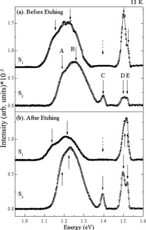
The PL spectra of un-etched samples S1 and S2 mea-sured at low temperature (11 K) are shown in Fig. 4(a). Spectra at same temperature of samples S1 and S2 af-ter etching the top-layer QDs are shown in Fig. 4(b). The energy features on PL for etching and un-etching cases spectra are a little different, but the major energy features are presented on both figures. The optical tran-sitions are labeled by symbols A, B, C, D and E, and
Fig. 4. Low temperature PL spectra of InGaAs/GaAs QDs with difference growth sequence ordering using migration en-hanced technique for samples S1 (In-Ga-As) and S2
(In-As-Ga-As). (a) Before removing the top QDs layer and (b) After removing the top QDs layer.
marked by arrows on peak positions shown in the fig-ures. Before etching the top-layer QDs of sample S1, the peak energy values EA and EB are 1.15 eV and 1.23 eV, respectively. The corresponding broadening parameters are 34 meV and 42 meV. After etching, the energy peak values EA and EB are 1.14 eV and 1.22 eV with broad-ening parameters 27 meV and 46 meV. The results show that the shape and particle size as well as the transition energy are slightly different. For un-etched sample S2, the energy peak values EA and EB are 1.19 eV and 1.25 eV with corresponding broadening parameters 23 meV and 51 meV. After etching, the transition energy values EA and EB are 1.19 eV and 1.25 eV with corresponding line-width parameters 23 meV and 47 meV. Like sample S1, the results of S2 show that the transition energy and broadening parameters are almost the same. It means the growth morphology of the QDs on top layer was less affected by the QDs grown on bottom layer covered with a 510-nm GaAs spacer. The average volume (particle size, height× diameter2) of the QDs on samples S
1 and S2measured with AFM are roughly to 4.3× 10³nm3and 3.5× 10³nm3. Thus the average particle size on sample S1is larger than that on sample S2. The results also show
A Study of Optical Properties of InGaAs/GaAs Quantum Dots – Chih-Ming Lai et al.
-S117-Table 1. Summary of the fitted results from PL spectra at low temperature (11 K). Symbols are denoted with UE (un-etched) and E (etched). The transition energy values in eV and broadening parameters in meV units.
Sample Transition energy features
EA ΓA EB ΓB EC ΓC ED ΓD EE ΓE UE 1.15 34 1.23 42 − − 1.50 11 1.52 4 S1 E 1.14 27 1.22 46 − − 1.51 14 − − UE 1.19 23 1.25 51 1.40 8 1.50 11 1.52 6 S2 E 1.19 23 1.25 47 1.40 8 1.50 15 1.52 6
that transition energy of S2 is higher than S1. We pro-pose that the EA and EB energy features are attributed to the optical transition of the ground state of the QDs with two kinds of QDs particle ensembles. The reason will be discussed in following next three paragraphs. The area density and homogeneity of S1 is better than S2.
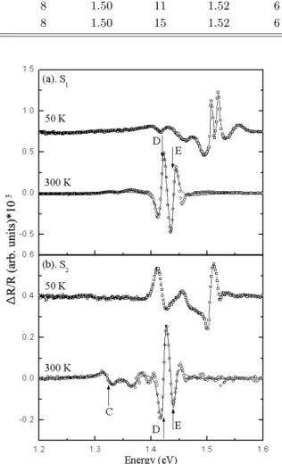
The energy value of the C peak is about 1.40 eV but is not present on sample S1. It is reasonable and consistent that sample S1 grew with higher average area density and larger average volume of the QD particle than those of sample S2. The energy feature of the InGaAs wetting layer on InGaAs/GaAs QD specimens was reported in the literature [22]. Therefore, the EC peak originates from the wetting layer. However, the peak disappears on sample S1due to the larger nano-particles (i.e. QDs). The energy values of the D and E peaks are about 1.50 eV and 1.52 eV for samples S1 and S2 without or with etching process. The broadening parameters are different and varied from 4 to 15 meV depending on the sample and etching process. The lower energy peak ED (1.50 eV) is attributed to the buffer layer and the higher energy peak EE (1.52 eV) originates from the GaAs cap layer. The fitted results are summarized and listed in Table 1. PR spectra carried out at room temperature and low temperature are shown in Fig. 5(a) for sample S1 and Fig. 5(b) for sample S2. The energy features are fit-ted by the third derivative function form (TDFF) with a Lorentzian line shape [24]. The energy peaks are labeled with the symbols C, D, and E corresponding to Fig. 4 and marked by an arrow notation on the peak position. Two energy values (D, E) fitted by a χ2 fitting method of TDFF Lorentzian line shape are 1.420 (1.423) eV and 1.439 (1.440) eV at room temperature for samples S1 (S2), respectively. The results summary is shown in Ta-ble 2. The energy features (D, E) are attributed to the
Table 2. Summary of TDFF fitted results from room-temperature PR spectra of un-etched samples S1and S2.
En-ergy values in eV and broadening parameters in meV units.
Transition energy features Sample
EC ΓC ED ΓD EE ΓE
S1 − − 1.420 9 1.439 10
S2 1.326 18 1.423 9 1.440 11
Fig. 5. PR spectra of InGaAs/GaAs QDs measured at room temperature (300 K) and low temperature (50 K) for samples (a) S1 and (b) S2.
buffer and cap layers of GaAs. The peak C originates from the InGaAs wetting layer. PR spectra measured at low temperature (50 K) display more energy features which are contributed to the InGaAs wetting layer, GaAs cap and buffer layers. These energy features could not be well fitted to the room-temperature PR spectra. The line shape of PR spectra also changed severely due to temperature cooling down below 50 K. PR spectra might provide more information after detailed line shape analy-sis which includes strain on GaAs layer. This needs more study in the future.
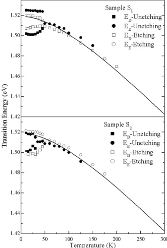
The transition energies measured with PL of low en-ergy portions (EA and EB) are plotted as a function of temperature for samples S1 and S2 (before etching) are
Fig. 6. Transition energies in the low energy portion mea-sured by PL experiment are plotted as a function of temper-ature on samples S1 and S2.
Table 3. Results summary of the fitted parameters using Varshni’s equation to fit the temperature-dependent transi-tion energy.
Sample Energy peak Parameters
S1 S2 Notes E (eV) 1.144 1.192 A α (×10−4eV/K) −5.9 −5.8 QDs1 β (K) 243 254 E (eV) 1.221 1.266 B α (×10−4eV/K) −8.7 −8.9 QDs2 β (K) 259 245 E (eV) − 1.401 C α (×10−4eV/K) − −3.5 WL β (K) − 253
shown in Fig. 6. The trends observed in EA (InGaAs QDs), EB(InGaAs QDs) and EC(InGaAs wetting layer) are different due to the temperature-dependent band-gap of InAs and GaAs materials. Because the wetting layer is an ultra thin InGaAs/GaAs quantum wells, the curve trend on the temperature will follow that of the host ma-terial of GaAs. However, the InGaAs QDs will be related to temperature behavior characteristic of the InAs and
Fig. 7. Transition energies in the high energy portion mea-sured by PL experiments is plotted as a function of temper-ature on samples S2 and S2.
GaAs materials. The optical properties of the InGaAs QDs and wetting layer were studied with the fitting pa-rameters using Varshni’s equation [26]. The summary of the fitting results are listed in Table 3. The argument of the peak identification was supported by this result. A slight abnormal behavior of the inverted ”S-curve” shape on temperature-dependent transition energies measured by PL spectra was observed. It has been explained by the carrier localization on potential minimum of In-rich island [27]. This effect could be studied by time-resolved PL spectroscopy in the future.
The transition energies of high-energy portion (ED and EE) for unetched samples S1 and S2 plotted as a functions of temperature are shown in Fig. 7. It clearly presents abnormal behavior in the inverted “S-curve” shape of the temperature-dependent PL transi-tion energy spectra. It shows that a red-shift then a blue-shift from the temperature range of 10 K to 50 K. This appears to be due to been the localization then de-localization of the charge carriers at on alloying local potentials [28,29]. This phenomenon happens commonly in III-V semiconductor alloys [30–32]. The spectra are difficult to fit using Varshni’s equation. However, a curve
A Study of Optical Properties of InGaAs/GaAs Quantum Dots – Chih-Ming Lai et al.
-S119-of the band-gap transition energy versus temperature for bulk GaAs material is plotted in the figure for reference.
IV. CONCLUSION
In0.5Ga0.5As/GaAs self-assembled QDs were grown with GS-MBE system by sequential and migration en-hanced epitaxial techniques. We analyzed these InGaAs QDs with SEM and AFM systems. The results show that the uniformity and density of QD sample S1 (In-Ga-As sequential growth ordering) is better than S2 (In-As-Ga-As). By AFM results, the QD size of S1 is greater than S2. The accurate particle size measurement would em-ploy with better accurate instruments (e.g. HR-TEM) in advanced study.
The major energy features of the PL spectra origi-nating from the a ground of the QD states and wetting layer as well as GaAs band-gap transitions have been identified and discussed. Two kinds of quantum dots, which are formed slightly different indium compositions, are proposed and interpreted corresponding to two peaks on PL spectra. An abnormal behavior of the inverted “S-shape” curve shown in the figure of the temperature-dependent transition energy is attributed to the carrier localization.
ACKNOWLEDGMENTS
The authors would like to thank Mr. C. H. Kao and Mr. C. W. Chang for their technical assistance to sup-port this study. This work was also supsup-ported finan-cially by the National Science Council (Taiwan) under the grant number NSC 90-2215-E-002-020 and NSC90-2215-E-002-021.
REFERENCES
[1] D. Bimberg, M. Grundmann and N. N. Leden-stov,Quantum Dot Heterostructures (Wiley, Chichester, 1998).
[2] Y. Toda, O. Moriwaki, M. Nishioka and Y. Arakawa, Phys. Rev. Lett. 82, 4114 (1999).
[3] F. Heinrichsdorff, Ch. Ribbat, M. Grundmann and D. Bimberg, Appl. Phys. Lett. 76, 556 (2000).
[4] N. Yokoyama, S. Muto, K. Imamura, M. takatsu, T. Mori, Y. Sugiyama, Y. Sakuma, H. Nakao and T. Adachihara, Solid State Electron. 40, 505 (1996). [5] G.Yusa and H. Sakaki, Appl. Phys. Lett. 70, 345 (1997). [6] I. N. Stranski and L. Krastanow, Akad. Wiss. Lit. Mainz
Abh. Math. Naturwiss. K1 IIb 146, 797 (1939). [7] D. Leonard, K. Pond and P. M. Petroff, Phys. Rev. B
50, 11687 (1994).
[8] D. Leonard, M. Krishnamurthy, C. M. Reaves, S. P. Denbaars and P. M. Petroff, Appl. Phys. Lett. 63, 3203 (1993).
[9] L. Goldstein, F. Glas, J. Y. Marzin, M. N. Charasse and G. Le Roux, Appl. Phys. Lett. 47, 1099 (1985). [10] S. Guha, A. Madhukar and K. C. Rajkumar, Appl. Phys.
Lett. 57, 2110 (1990).
[11] J. M. Moison, F. Houzay, F. Barthe, L. Leprince, E. Andre and D. Vatel, Appl. Phys. Lett. 64, 196 (1994). [12] A. Tackeuchi, Y. Nakata, S. Muto, Y. Sugiyama, T. Inata
and N. Yokoyama, Jpn. J. Appl. Phys. 34, L405 (1995). [13] P. B. Joyce, E. C. Le Ru, T. J. Krzyzewski, G. R. Bell, R. Murray and T. S. Jones, Phys. Rev. B 66, 75316 (2002). [14] A. A. Darhuber, V. Holy, J. Stangl, G. Bauer, A. Krost, F. Heinrichsdroff, M. Grundmann, D. Bimberg, V. M. Ustinov, P. S. Kop’ev, A. O. Kosogov and P. Werner, Appl. Phys. Lett. 70, 955 (1997).
[15] R. P. Mirin, J. P. Ibbetson, K. Nishi, A. C. Gossard and J. E. Bowers, Appl. Phys. Lett. 67, 3795 (1995). [16] S. Farfad, R. Leon, D. Leonard, J. L. Merz and P. M.
Petroff, Phys Rev. B 52, 5752 (1995).
[17] J. M. Garcia, G. Medeiros-Ribeiro, K. Schmidt, T. Ngo, J. L. Feng, A. Lorke, J. Kotthaus and P. M. Petroff, Appl. Phys. Lett. 71, 2014 (1997).
[18] Q. D. Zhuang, J. M. Li, H. X. Li, Y. P. Zeng, L. Pan, Y. H. Chen, M. Y. Kong and L. Y. Lin, Appl. Pys. Lett. 73, 3706 (1998).
[19] L. Chu, M. Zrenner, M. Bichler, G. Bohm and G. Ab-streiter, Appl. Phys. Lett. 77, 3944 (2000).
[20] P. W. Fry, I. E. Itskerich, D. J. Mowbray, M. S. Skolnick, J. J. Finley, J. A. Barker, E. P. O’reilly, L. R. Wilson, I. A. Carkin, P. A. Maksym, M. Hopkinson, M. Al-khafari, J. P. R. David, A. G. Gullis, G. Hill and J. C. Clark, Phys. Rev. Lett. 84, 733 (2000).
[21] J. J. Finley, M. Skalitz, M. Arzberger, A. Zrenner, G. Bohm and G. Abstreiter, Appl. Phys. Lett. 73, 2618 (1998).
[22] L. Chu, M. Zrenner, G. Bohm and G. Abstreiter, Appl. Phys. Lett. 76, 1944 (2000).
[23] P. D. Siverns, S. Malik, G. McPherson, D. Childs, C. Roberts, R. Murray and B. A. Joyce, Phys. Rev. B 58, R10127 (1998).
[24] F. H. Pollak, in Handbook on Semiconductors, edited by Balhanski (North-Holland, New York, 1993), Vol. 2. [25] S. M. Kim, S. H. Lee, H. W. Kim, J. K. Shin, J. Y. Leem,
J. S. Kim and J. S. kim, J. Korean Phys. Soc. 40, 119 (2002).
[26] S. H. Cho, Y. K. Choi and E. K. kim, J. Korean Phys. Soc. 37, 1030 (2000).
[27] K. L. Teo, J. S. Colton, P. Y. Yu, E. R. Weber, M. F. Li, W. Li, K. Uchida, H. Tokunaga, N. Akutsu and K. Matsumoto, Appl. Phys. Lett. 73, 1697 (1998).
[28] M. Kondow, S. Minagawa, Y. Inoue, T. Nishino and Y. Hamakawa, Appl. Phys. Lett. 54, 1760 (1989).
[29] M. Kondow and S. Minagawa, J. Appl. Phys. 64, 793 (1988).
[30] M. Kasu, T. Yamamoto, S. Noda and A. Sasaki, Jpn. J. Appl. Phys. 29, 828 (1990).
[31] F. A. J. M. Driessen, G. J. Bauhuis, S. M. Olsthoorn and L. J. Giling, Phys. Rev. B 48, 7889 (1993).
[32] U. H. Lee, J. S. Yim, D. Lee, H. G. Lee, S. K. Noh, J. Y. Leem and H. J. Lee, J. Korean Phys. Soc. 37, 593 (2000).