567 (Received August 14, 1998; accepted November 20, 1998)
Department of Electronics Engineering, National Chiao-Tung University, Hsinchu, Taiwan
Copper chemical vapor deposition from Cu(hexafluoroacetylacetonate)trimethyl-vinylsilane (Cu(hfac)TMVS) was studied using a low pressure chemical vapor deposition system of a cold wall vertical reactor. The Cu films deposited using H2 as a carrier gas revealed no impurities in the films within the detection limits of Auger electron spectroscopy and x-ray photoelectron spectroscopy. Using hydrogen as a carrier gas, the hydrogen not only acts as a reducing agent, but also reacts with the residual fragment of precursor. As a result, using H2 as a carrier gas for Cu(hfac)TMVS resulted in Cu films of lower resistivity, denser microstructure and faster deposition rate than using Ar or N2 as the carrier gas. Moreover, we found that N2 plasma treatment on the substrate surface prior to Cu deposition increased the deposition rate of Cu films.
Key words: Chemical vapor deposition (CVD), Cu films, H2 as carrier gas, resistivity
INTRODUCTION
With the continuing progress of ultra large scale integrated (ULSI) circuits, the feature sizes of vias and holes in multilevel metallization structures have decreased to sub-quarter micron, while the associated aspect ratios have increased to four and higher. Eventually, however, the continuing scale down of active devices becomes less profitable, as the limitations of the circuit speed and maximum functional density become more dependent on the characteristics of interconnects than on the scaled devices. Thus, the conventional physically vapor deposited, aluminum-based interconnect scheme faces various performance and reliability challenges.1–4
Hence, new interconnect metals and their processing techniques must be studied and developed. Chemical vapor deposition of copper has been one of the most promising approaches. Copper has a resistivity lower than aluminum (bulk resistivity of 1.7 vs 2.7µΩ-cm), which significantly reduces the RC time delay. The electro/stress migration resistance of copper has been reported to be two orders of magnitude better than that of aluminum, and thus higher reliability and improved performance can be expected by using copper interconnects.5–7 Moreover, it has been demonstrated
that the technique of chemical vapor deposition (CVD)
of copper possesses an intrinsic potential for void free filling of aggressive via and hole structures at near bulk resistivity and high growth rates.8,9
However, in spite of significant progress in the development of copper based metallization schemes, several key processing and reliability issues remain to be resolved before copper technology becomes an industrial reality. Among them, the development of a CVD process capable of depositing high purity and dense films of copper with controlled microstructure at relatively low temperatures with high deposition rates is of vital interest for practical applications.
In this work, copper chemical vapor deposition from Cu(hexafluoroacetylacetonate) trimethylvinylsilane (Cu(hfac)TMVS)10,11 was studied with emphasis on
the role of H2 as a carrier gas. The effects of substrate surface treatment by N2 plasma were also investigated.
EXPERIMENT
A cold-wall, low pressure CVD system of vertical reactor was employed to deposit Cu films using Cu(hfac)TMVS as the precursor. The Cu films were deposited on TiW substrates. A TiW layer of 100 nm thickness was deposited on p-type, (100)-oriented Si wafers by sputtering using a TiW (Ti 10 wt%) target in an Ar ambient at a pressure of 5 × 10⁻³ Torr and with
a deposition rate of 10 nm/min. The base pressure prior to the sputter deposition was 1.2 × 10⁻⁶ Torr. The
and then rinsed in deionized water for 5 min. The substrates were then dried with N2 gas and immediately loaded into a loading chamber before they were loaded in the CVD chamber. When the loading chamber was pumped down to a pressure of 10–7 Torr, which is nearly equal to the pressure in the
reaction chamber, the substrates were transferred to the substrate holder in the reaction chamber. The Cu
CVD was performed over a temperature range of 160 to 240°C and a pressure range of 70 to 1000 mTorr. In this study, the precursor was maintained at a temperature of 40°C, and the carrier gas (H2, Ar or N2) was bubbled through the liquid Cu(hfac)TMVS precursor to carry the Cu source into the reaction chamber via a delivery line kept at a temperature of 60°C. When the deposition was completed, the samples were cooled in the ambient of carrier gas at a pressure of 10 Torr.
The Cu film thickness was measured using a Dek-Tek profiler on a step created on the film and was further confirmed by the cross-sectional scanning electron microscope (SEM) examination. A four-point probe was employed to measure the sheet resistance. SEM was also used to observe the surface morphology of the Cu films. Both Auger electron spectroscopy (AES) and x-ray photoelectron spectroscopy (XPS) were used to analyze the impurity content in the Cu films. Transmission electron microscope (TEM) was used to examine the microstructure of the Cu films, and x-ray diffiaction (XRD) analysis was used for crystal phase identification.
RESULTS AND DISCUSSION
Copper films were deposited to thicknesses of 0.5 to 1.0 µm on TiW substrates with good adhesion; the thickness of the films deposited were measured using a Dek-Tek profiler on a step created on the film and were confirmed by SEM examination. The as-deposited Cu films revealed carbon (C) and oxygen (O) contamination on the surface regions, as shown in the XPS spectrum of as-deposited Cu films illustrated in
Fig. 1. XPS spectrum of as-deposited Cu films on TiW substrates.
Fig. 4. XPS spectrum of Cu films showing Cu(2p1/2) and Cu(2p3/2) peaks.
Fig. 2. XPS spectrum of Cu films on TiW substrates after removal of about 25 nm thick surface layer by Ar-ion sputtering.
Fig. 3. Typical differential AES spectrum of Cu films on TiW substrates after removal of about 25 nm thick surface layer by Ar-ion sputtering.
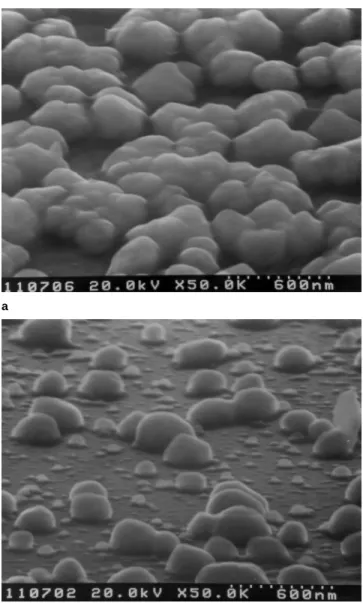
deposition were minimal. The contamination of C and slightly different characteristics, such as the rate of nucleation, film resistivity, impurity content, and microstructure. Figure 5 shows the SEM micrographs of Cu films deposited using two different carrier gases, H2 and Ar. Both were deposited on TiW substrates at a temperature of 200°C and a pressure of 500 mTorr using a carrier gas flow rate of 20 sccm and a deposition time of 10 min. The nucleation rate of Cu with H2 as the carrier gas was faster than that with Ar as the carrier gas. Table I shows that different carrier gases resulted in different resistivities and deposition rates. The film resistivity was determined by sheet resistance measurement and film thickness measurement, while the deposition rate was determined by averaging the thicknesses of the films deposited with the deposition time. Hydrogen can react with the by-product of the Cu precursor in the following way
H2 + Cu(hfac)2→ 2Hhfac+Cu
Thus, the deposition rate of Cu films using H2 as the carrier gas is faster than using an inner gas such as Ar and N2. Moreover, since H2 can react with the residual fragment of precursor, the impurity content in Cu films was reduced significantly. The carrier gas H2 will not only act as a reducing agent,13–15 thus leading
to an increase in deposition rate, but also react with the residual precursor fragments, thereby leading to reduced impurity contents in Cu films.13,14 This in
turn causes lower resistivity in Cu films. It is obvious that H2 plays a role of promoter as well as cleanser.16,17
Figure 6 shows the TEM micrographs of Cu films deposited using three different carrier gases, H2, Ar, and N2. All were deposited on TiW substrates at 200°C and 500 mTorr using a carrier gas flow rate of 100 sccm. Using different carrier gases resulted in Cu films with different microstructures. Copper films deposited using H2 as a carrier gas have a denser microstructure with smaller grain size, while the Cu films deposited using Ar or N2 as a carrier gas displayed much bigger grains which appear to be agglomerated from many smaller grains. Figure 7 shows SEM micrographs of Cu films deposited using Ar as a carrier gas, indicating that Cu tended to nucleate on the Cu nuclei. Thus, the big grains shown in Fig. 6b and 6c are likely accumulation of Cu nuclei. From residual gas analysis conducted during deposition, we have found different hydrogen levels depending on the substrate used. We presume that hydrogen may be attracted to the surfaces of conductor substrates from a chemical mechanism, with subsequent
Fig. 5. SEM micrographs of Cu films deposited on TiW at 200°C and 500 mTorr using (a)H2 and (b)Ar as the carrier gas; the flow rate of carrier gas is 20 sccm and the deposition time is 10 min.
Table I. Deposition Rate and Electrical Resistivity of Cu Films Deposited
using Different Carrier Gases
Carrier Gas H2 Ar N2
Resistivity (µΩ-cm) 2.85 4.5 3.3 Deposition Rate (Å/min) 162 128 145 b
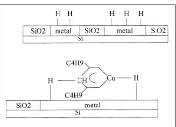
chemisorption of the β-diketonate precursor through direct bonding between the surface H and the CH radical in the precursor. This forms CH2,18 as
illustrated in Fig. 8. The precursor then decomposes, yielding a Cu-H thin layer which proceeds with
Fig. 7. SEM micrographs of Cu films deposited on TiW at 200°C and 500mTorr with 100 sccm carrier gas flow rate of Ar for a deposition time of (a)5 and (b)10 min.
desorption of the precursor byproducts. The copper layer then grows on this “seed” CuH layer. It is this hydrogen adsorption effect that allows Cu films deposited using H2 as a carrier gas to have a denser microstructure (Fig. 6). The hydrogen causes formation of denser Cu nuclei on the substrates from the initial nucleation stage (Fig. 5). Without this “seed” Cu-H layer, the preferential nucleation of Cu on the Cu nuclei results in agglomeration, bigger grains, and lower deposition rate as observed when using Ar or N2 as a carrier gas. In fact, preferential adsorption of hydrogen to conductor substrates, but not to insulator substrates, is the key factor in the selective growth of Cu CVD.18
Figure 9 shows the XRD spectrum of a 1 µm thick Cu film deposited on TiW substrate at a pressure of 500 mTorr, indicating a polycrystalline structure. We found from the XRD analysis that all Cu films deposited in this work, regardless of deposition temperature, have a structure of the fcc Bravais lattice. We also found that Cu films deposited at higher temperatures contain a more porous microstrucure. These pores have the effect of increasing the resistivity of Cu films.
Since the substrate surface conditions play an
Fig. 6. TEM micrographs of Cu films deposited on TiW at 200°C and 500mTorr with 100sccm carrier gas flow rate of (a) H2, (b) Ar, and (c) N2.
Fig. 8. Effects of hydrogen adsorption on the copper deposition (a) adsorption of hydrogen to the conductor substrate surfaces, and (b) adsorption of precursor to the substrate surfaces through a direct bonding with the surface hydrogen.
a b c
important role in CVD of Cu films, it is anticipated that a plasma treatment on the substrate surfaces prior to the Cu deposition should have beneficial effects on the deposition of Cu films.19 In this work, N
2
plasma was used for substrate surfaces treatment. Figure 10 shows the Cu film thickness as a function of deposition temperature for the TiW substrates with and without N2 plasma treatment. The N2 plasma was performed ex situ, in a reactor (ULVAC ERA 1000S) at a power of 100 W with an N2 flow rate of 80 sccm. It is obvious that the N2 plasma treatment modified the substrate surfaces, resulting in an increase in nucleation rate and growth of Cu films.
surface substantially increased the deposition rate of Cu films.
REFERENCES
1. A. Jain, T.T. Kodas, R. Jairath and M. J. Hampden-Smith, J.
Vac. Sci. Technol. B 11, 2107 (1993).
2. A.F. Burnett and J.M. Chech, J. Vac. Sci. Technol. A 11, 2970 (1993).
3. N. Awaya and Y. Arita, J. Electron. Mater. 21, 959 (1992). 4. Y. Arita, Mater. Res. Soc. Symp. Proc. VLSI V (Pittsburgh,
PA: Mater. Res. Soc., 1990), p. 337.
5. P.L. Pai and C.H. Ting, IEEE Electron Device Lett. EDL-10, 423 (1989).
6. The Chemistry of Metal CVD, ed. T.T. Kodas and M. J. Hampden-Smith (VCH Weinheim, 1994).
7. A. Jain, K.M. Chi, H.K. Chi, J. Farkas, T.T. Kodas and M.J. Hampden-Smith, Semicond. Int., 16 (June 1993), p.128. 8. W. Lee and R. Reeves, J. Vac. Sci. Technol. A 9, 653 (1991). 9. J. Halstead, P. Locke and R. Reeves, Mater. Res. Soc. Symp.
Proc. 260 (Pittsburgh, PA: Mater. Res. Soc., 1992), p. 647.
10. J.C. Chiou, Y.J. Chen and M.C. Chen, J. Electron. Mater. 23, 383 (1994).
11. J.A. T. Norman, B.A. Murator, P. N. Dyer, D.A. Roberts and A.K. Hochberg, J. Phys. IV, Colloque, C2, 271 (1991). 12. J. Li, Y. Shacham-Diamand and J. Mayer, Mater. Sci. Rep. 9,
1 (1992).
13. N. Awaya and Y. Arita, 1989 Symp. VLSI Technol. (IEEE Electron Device Society, Kyoto, Japan, 1989), p. 103. 14. Y. Arita, N. Awaya, K. Ohno and M. Sato, IEDM Tech. Dig. 39
(1990).
15. A.E. Kaloyeros, A. Feng, J. Garhart, K.C. Brooks, S.K. Ghosh, A.N. Saxena and F. Luehrs, J. Electron. Mater. 19, 271 (1990).
16. N. Awaya and Y. Arita, Thin Solid Films 262, 12 (1995). 17. W.W. Lee, and P.S. Locke, Thin Solid Films 262, 39 (1995). 18. A.E. Kaloyeros, C. Dettelbacher, E.T. Eisenbraun, W.A. Lanford and P.J. Toscano, Mater. Res. Soc. Symp. Proc. 229 (Pittsburgh, PA: Mater. Res. Soc., 1991), p.123.
19. G. Braeckelmann, D. Manger, A. Burke, G. G. Peterson and A. E. Kaloyeros, J. Vac. Sci. Technol. B 14, 1828 (1996).
Fig. 10. Cu film thickness as a function of deposition temperature for the TiW substrates with and without N2 plasma treatment.