3B-3
Performance of MOCVD Tantalum Nitride Diffusion Barrier for
Copper Metallization
S.C.
Sun,
M.H. Tsai, C.E. Tsai*,
and
H.T.
mu*
National Nan0 Device
Laboratory
and
Departmentof Electronics Engineering
*Instituteof
Applied
ChemistryNational
ChiaoTung
University,Hsinchu, Taiwan,
R.O.C.
Abstract
A low-resistivity and low carbon concentration CVD TaN film has been realized by using a new precursor terbutylimido-tris-diethylamido tantalum W T D E T ) . Results show that CVD TaN as a diffusion barrier for Cu has higher thermal stability up to 500 "C than CVD TiN of 450 "C.
Introduction
Refractory metal nitrides such as
TiN
and TaN have beenstudied to establish thermally stable and adhesive metallization schemes with low resistivity [ 1,2]. However, these metal nitride materials have been deposited via reactive sputtering of Ti and Ta targets in an Ar-N, atmosphere where the step coverage degrades rapidly as the aspect ratio of the features becomes greater than one. Accordingly, there has been a growing interest in developing CVD processes for deposition of refractory metal nitride thin films. One recent investigation of interdiffusion in Cu/CVD TIN thin-film structures found that the LPCVD TiN was stable up to 450 "C
for 30 minutes only, after which Cu started to diffuse into the TiN layer [3]. Our interest is to develop an alternative CVD metal nitride which can withstand Cu diffusion at a higher sintering temperature. An attempt to grow CVD TaN by using Ta(NMe2)5 and ammonia chemistry has resulted tetragonal phase T%N, film, which is known as a dielecmc material with very high resistivity (>lo6 p a - c m ) [4]. Such high resistivity hampers its usefulness as diffusion barrier for advanced metallization. In this work, low-resistivity TaN thin films are deposited by LPCVD method using a new metal-organic precursor
TBTDET.
Experimental
Fig. 1 shows the molecular structure of TBTDET Ta=NBu (NEt,),. Strong Ta=N double bond has preserved the "TaN" portion of the precursor and results in a cubic phase TaN film during the pyrolysis process. The depositions were carried out in a cold-wall low pressure reactor with the base pressure of lo-, torr. The source was vaporized at 40 to 50 OC. Typical deposition pressure was 20 mtorr.
t
Results
and
DiscussionFig. 2 shows the dependence of deposition rate and film resistivity on the wafer temperature. The deposition rate was largely independent of the substrate temperature possibly indicating a source-limited reaction. Higher deposition temperatures yield lower resistivities. The lowest resistivity obtained was 600 p a - c m at a source temperature of 45 O C and
substrate temperature of 600 "C. These values are in the range of sputtered TaN (200-1000 pLR-cm). Fig. 3 shows the XRD
pattems of CVD TaN deposited at various temperatures. The
major Cu K, peaks are comparable to those of cubic TaN, i.e.
( l l l ) , (200), (220), (311) reflections at 35.84, 41.59, 60.40
and 72.22', respectively [ 5 ] . The XRD peaks for 500 "C deposited films were broad, presumably due to the presence of small grain microstructures or carbon impurities. Fig. 4 shows the XPS depth profiles of TaN films deposited at 600
"C. It revealed 10 at.% carbon and 5 at.% oxygen in the film.
The T a 4f5,, and 4f7,2 peak shifts in the Ta 4f region were consistent with published stoichiometric TaN data [6].
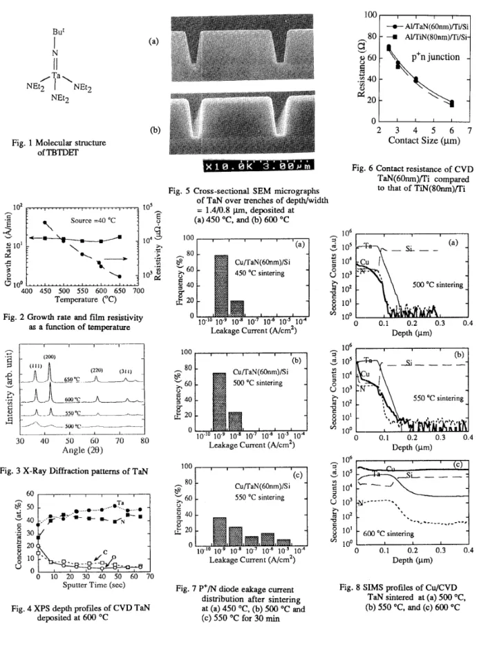
Fig. 5(a) and (b) show the SEM micrographs of 60-nm
TaN deposited at 450 and 600 "C. The 450 "C film had nearly 100% step coverage and no obvious grain structures. At 600
"C the coverage was reduced to 40%, but still demonstrated an excellent continuity around comer region of the bottom of the contact. The film also showed grain boundary with columnar structures.
By using Ti as an ohmic contact layer, we measured contact resistance of Al/T'aN/Ti with reference to AfliN/T'i. As shown in Fig. 6, TaN (60 nm) displayed equivalent contact resistance compared to sputtered TiN (80 nm). This is because CVD TaN has better bottom coverage than reactive-sputtered TiN.
In order to fiid the thermal stability of CVD TaN as a barrier layer against Cu diffusion, leakage current was measured as the wafers were stressed sequentially at 450, 500
and 550 OC in vacuum for 30 min at each temperature.
As
shown in Fig. 7, leakage current remains stable up to 500 "C. For samples sintered at 500°C, Cu appears to have stayed within the TaN film as indicated in the SIMS profiles of Fig.
8. The
breakdown of TaN occurs at 600 "C. It is plausible that the nitrogen impurities in TaN grain boundaries and nitrogen atoms located at interstitial sites of cubic TaN structure block the diffusion paths of Cu and Si, resulting in a higher interdiffusion temperature.
C o n c l u s i o n s
We have demonstrated that MOCVD TaN is an excellent barrier material with a good step coverage, low resistivity, low leakage current and high thermal stability.
T h e experimental results indicate that TaN film prevents the interdiffusion of Cu and Si up to 500 "C for 30 min, which is more improved than the previous report on a CVD TiN diffusion barrier.
At 550 OC Cu begins to intrude through TaN.
References
[l] M. Wittmer, J .
VUC.
Sci, Technol. A 3, 1797 (1985)[Z] M.A. Faroo, et al., J . Appl. Phys., 7 0 , 1369 (1991) [3] J.O. Olowolafe et al., J . Appl. Phys.. 72, 4099 (1992) [4] R. Fix et al., Chem. Muter., 5, 614 (1993)
[5] JCPDS, Powder Diffraction File No. 32-1283 (1982) [6] K. Sasaki et al., Jpn. J . Appl. Phys., 29, 1043 (1990)
But
N
I
II
/a\ NEt21
NEt2 NEt2Fig. 1 Molecular structure
O f T B T D E r
."
400 450 500 550 600 650 700
Temperature ("C) Fig. 2 Growth rate and film resistivity
as a function of temperature
I I 1
-1'.A 500 "C
30 40 50 60 70 80
Angle (28)
3 X-Ray Diffraction patterns of TaN
$
so
____ *
... .-T a.....
J....*..;
t- 3 40 ,...p' . 'c 30 J o--
- - D - - O J__
v o
;U
$
10 0 * * 10 - - 20 30 40 SO 60 70Sputter Time (sec) Fig. 4 XPS depth profiles of CVD TaN
deposited at 600 OC L 00 I I I I -e- Al/TaN(60nm)/Ti/Si
p+n junction
.\
2 3 4 5 6 7Contact Size
(pm)
Fig. 6 Contact resistance of CVD TaN(60nm)ni compared to that of TiN(80nm)ni Fig. 5 Cross-sectional SEM micrographs
of TaN over trenches of dem.h/width = 1.410.8 pm, deposited at (a)
450
"C, and @) 600 "C Cu/TaN(60nm)/S i 1 Leakage Current (~/cm') Cu/TaN(60nm)/S i 0 0.1 0.2 0.3 0.4 Depth(k"
106.
10'i
3
104S
103 U9
10'8
10' 1 v1v,
IO0 Leakage Current ( A h 2 ) CuRaN(60nm)/S i SS0 "C sinteringFig. 7 P+/N diode eakage current distribution after sintering at (a) 450 O C , (b) 500 O C and (c) 550 "C for 30 min
v.---..
600 ' C sinteringi
'"-L
A
0 0.1 0.2 0.3 0.4 Depth (PIFig. 8
SIMS
profiles of Cu/CVDTaN sintered at (a) 500 OC, (b) 550 OC, and (c) 600 'C