IEEE PHOTONICS TECHNOLOGY LETTERS, VOL. 20, NO. 2, JANUARY 15, 2008 141
One-Shot Exposure for Patterning Two-Dimensional
Photonic Crystals to Enhance Light Extraction of
InGaN-Based Green LEDs
Mei-Li Hsieh, Kuo-Chang Lo, Yi-Sheng Lan, S. Y. Yang, C. H. Lin, H. M. Liu, and
H. C. Kuo, Senior Member, IEEE
Abstract—To promote the feasibility of using photonic crystals
to enhance light extraction of light-emitting diodes (LEDs) for industrial applications, the request for the high-yield and simple exposure process to pattern two-dimensional photonic crystals (2DPCs) becomes rather urgent. In this work, we developed a one-shot three-beam laser interference system to fabricate a 2DPC on an InGaN-based green LED to address its performance for backlight display applications. Using the current exposure system we develop here, a submicro-patterned area of 6 mm in diameter can be achieved. The experimental results show that the operating voltage of a1 2 1 mm2in-area LED incorporated with the 2DPC is around 4 V, and the light extraction efficiency is enhanced by a factor of 2.1.
Index Terms—Holography, light-emitting diode (LED), photonic
crystal.
I. INTRODUCTION
A
NEW era in illumination technology has been unleashed since Nakamura succeeded in creating the first blue GaN-based light-emitting diode (LED) in 1993. In the past decade, enhancements in the efficiency and reliability of LEDs with dif-ferent colors, as well as effective reductions in LED manufac-turing costs, have continued to be exciting areas of research and development. This is especially true, given that the demand for white LEDs continues to accelerate, because of the wide use of white LEDs in a multitude of consumer electronics, including televisions, hand-held devices, and various indoor and outdoor lighting displays.There are currently several ways of producing white LEDs. In the case of the red–green–blue LED method, the potential of generating white light with a wider color gamut, especially for liquid-crystal-display back-lighting and projector applications, is rather promising. However, the main challenge remains the
Manuscript received June 5, 2007; revised September 12, 2007. This work was supported by the NSC under Grant NSC 94-2622-E-003-004-CC3, Grant 95-2221-E-003-015, and Grant 95-2112-M-003-017-MY2.
M.-L. Hsieh, K.-C. Lo, Y.-S. Lan, and S. Y. Yang are with the Institute of Electro-optical Science and Technology, National Taiwan Normal University, Taipei 116, Taiwan, R.O.C. (e-mail: [email protected]).
C. H. Lin is with Mesophotonics Limited, Southampton, SO16 7NP, U.K. H. M. Liu is with Epistar Corporation, Hsinchu 300, Taiwan, R.O.C. H. C. Kuo is with the Institute of Electro-Optical Engineering, National Chiao Tung University, Hsinchu 300, Taiwan, R.O.C.
Color versions of one or more of the figures in this letter are available online at http://ieeexplore.ieee.org.
Digital Object Identifier 10.1109/LPT.2007.912510
performance of green LEDs because of the inherent lower ef-ficiency of InGaN-based green LEDs, as compared to the effi-ciency of red and blue LEDs.
Photonic crystals have been the subject of a great deal of attention in the LED industry because of their promising effect on enhancing the extraction efficiency of LEDs [1]–[3]. Several groups have incorporated two-dimensional photonic crystal (2DPC) structures on LED surfaces to effectively extract light out of high dielectric LED materials [4]–[8]. In those groups’ re-ports, e-beam lithography has been the most popular technology used to fabricate submicrometer structures for 2DPC on LED surfaces. Recently, Kim et al. developed a 2DPC with rectangular arrays of holes on GaN-based LEDs using two-step holographic exposure technology to rotate LED samples by 90 [9]. How-ever, it is preferable that 2DPCs with triangular arrays of holes are fabricated on LED wafers, since the multifold symmetry of 2DPC geometry enhances LED light extraction [10]. It is well known that the pattern of 2-D triangular arrays can be achieved via three-beam-interference technology [11], [12]. Therefore, in this work, we developed a one-shot laser holographic exposure involving three-beam-interference technology for patterning a triangular-arrayed 2DPC on InGaN-based LED, and investigated the characteristics of the formed 2DPC green LED.
II. EXPERIMENTALDETAILS
The InGaN-based green LED structure, from bottom to top, consisted of a 50-nm-thick GaN nucleation layer on a sapphire substrate, a 3- m-thick Si-doped n-GaN buffer layer, an un-intentionally doped InGaN–GaN multiple quantum-well active region, a 50-nm-thick Mg-doped p-AlGaN electron blocking layer, a 0.25- m-thick Mg-doped p-GaN contact layer, and a Si-doped n-InGaN–GaN short-period superlattice structure. To efficiently transfer the 2DPC pattern from the photoresist to p-GaN layer, a SiO layer was deposited on the p-GaN layer. Then, photoresist Shipley S-1805 was spread on the SiO layer. The schematic diagram of the three-beam interference system developed in this work is shown in Fig. 1. An expanded laser beam, 6 mm in diameter, passed through two beam splitters to be divided into three coherent beams. These three beams were aligned to intersect symmetrically and generate a 2-D interfer-ence pattern on the wafer [13]. The three incident beams had the same polarization orientation, and the intensities of the incident beams were equal. For the periodic pattern, the period d can be manipulated by adjusting the angle between any two incident beams and the wavelength of the incident beam via
(1)
142 IEEE PHOTONICS TECHNOLOGY LETTERS, VOL. 20, NO. 2, JANUARY 15, 2008
Fig. 1. Schematic diagram of the laser interference system with three beams.
To extract green light (wavelength 540 nm) from the top layer, i.e., p-GaN, of LED, the minimum value for is 253 nm for air-hole photonic crystals with a filling factor around 0.3 according to photonic-band-structure calculation (not shown here). Here, for easy alignment in the holographic exposing system, the was designed to be from 400 to 450 nm. In that case, the green light is extracted by leakage modes when the light propagates along the 2-D air-hole photonic crystal.
To achieve as 400–450 nm, a 355-nm wavelength laser was used, with the angle set at 57 . As a result, 430 nm can be expected to be the period via (1). Remarkably, an area triangular 2DPC that is 6 mm in diameter can be generated on the coated photoresist via our one-shot exposure system.
Due to the finite volume of each constructive interference spot, the exposed depth may be less than the thickness of the photoresist layer. This may lead to the existence of residual pho-toresist at constructive interference spots, which would in turn suppress the etching of the SiO layer beneath the photoresist layer. To remove such residual photoresist at constructive inter-ference spots, a wafer covered with patterned 2DPC photoresist was treated with Ar-mixed O plasma for a few seconds. Gases composed of 30 sccm of CHF and 2 10 sccm of O were then used to etch the SiO layer under the conditions of 100-W induc-tive coupled plasma (ICP) power and 50-W reacinduc-tive-ion-etching (RIE) power. Before GaN etch, the photoresist removal was per-formed by acetone. The GaN etch was processed in use of the main etch gases of chlorine, methane, and CH together with an RF power of 125-W ICP and 100-W RIE. The etching ratio of p-GaN to SiO could be over 10, therefore, a thin SiO layer should be enough to achieve a deep p-GaN etch. Finally, the remaining SiO was removed by steeping it in 1 : 5 BOE. The depth of etched hole is about 120 nm from the cross section of the image taken with a scanning electron microscope [(SEM) not shown here].
For white light display applications, we processed the submicro-structured LED wafer into high-power chips, of which each had areas of mm . To improve current spreading, cross-finger-type electrodes were defined by stan-dard photolithography. A 300-nm-thick indium–tin–oxide (ITO) layer was subsequently evaporated at 300 C onto the LED wafer to serve as a transparent conducting layer. A layer of SiO with a thickness of 250 nm was then deposited on the ITO layer for passivation. Finally, Cr–Au contact was deposited onto the sample to serve as electrodes.
In the electroluminescence measurement, a continuous cur-rent was injected into the device at room temperature. A
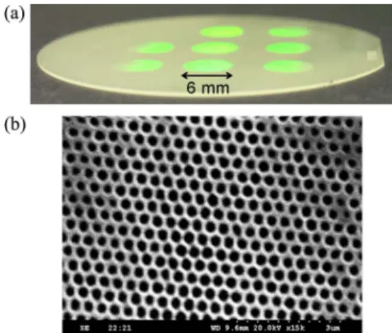
cal-Fig. 2. (a) Macroscopic view of eight spots with 2DPC on a 2 GaN wafer. (b) Typical SEM image of the microstructure of the 2DPC on the p-GaN layer.
ibrated area Si photodiode placed 5 mm above the device de-tected the light output. This detection setup captured almost all the power emitting from the LED.
III. RESULTS ANDDISCUSSION
Fig. 2(a) shows the macroscopic view for eight spots of quarter-inch-in-diameter 2DPC on a wafer. The spots became green due to the diffraction of the incident white light by the 2DPC. It is clear that the diameter of the each 2DPC spot was about 6 mm. A typical magnified image of the microstructure of a 2DPC spot taken by an SEM is shown in Fig. 2(b). Although the diameter of each spot achieved with the one-shot exposure is 6 mm, a large-area 2DPC can be obtained by step-and-repeat over the whole wafer, as shown in Fig. 2(a).
Through the photonic-band-structure calculation for a hole-type 2DPC p-GaN slab, the longest wavelength for the omni-directional leakage modes of the 2DPC was estimated around 1100 nm. Thus, the green light—540 nm in wave-length—emitted by the LED was in leakage mode when propa-gating along the 2DPC in the p-GaN layer. This demonstrates that there is a possibility of extracting more green light from the InGaN-based LED with the help of the 2DPC on the p-GaN surface. In comparison, a regular LED, with an area of 1 mm , (denoted as “LED”) and a 2DPC-integrated LED (denoted as “PCLED”) were chosen from the chips located spatially close to each other on the same wafer and were then packaged onto TO cans for electric and optical characterizations.
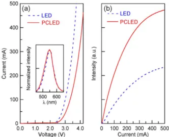
To get the extraction improvement, the sampling rule was picking up PCLEDs inside the interference spot and LEDs just outside that chosen spot. Five samples with the same wavelength for each type from two different spot locations were chosen in this study. Then the samples packaged onto TO-cans were put inside an integration sphere; therefore, the total power of the samples was measured. Fig. 3(a) shows the averaged current–voltage characteristics of LED and PCLED. At a driving current of 350 mA, the working voltages for the LED and PCLED were 3.55 and 4.03 V, respectively. The higher voltage of PCLED was due to the poor ITO step cov-erage on the submicro-patterned p-GaN surface. However, the working voltage of around 4 V is still acceptable for practical applications and can be improved by tuning the ITO deposit rate and temperature. Fig. 3(b) plots the current dependent illuminant intensity ( – curve) for both the LED and PCLED.
HSIEH et al.: ONE-SHOT EXPOSURE FOR PATTERNING 2DPCs TO ENHANCE LIGHT EXTRACTION 143
Fig. 3. (a) Current–voltage characteristics and (b) current dependent illuminant intensity of LED (dashed line) and PCLED (solid line) chips. The inset shows the emitting spectra of LED and PCLED chips at driving current of 350 mA.
Fig. 4. Normalized light–output radiation patterns of LED (dashed line) and PCLED (solid line) chips at driving current of 350 mA.
Obviously, the – curve of PCLED moved to the region having a larger illuminant intensity. This reveals the fact that the light extraction from LED was definitely enhanced via the fabricated 2DPC on the top p-GaN layer. At the driving current of 350 mA, compared with the LED, the illuminant intensity of PCLED was increased by a factor of 2.1. It is worth noting that, in the inset of Fig. 3(a), the emitting spectrum of PCLED biased with 350 mA shares the same characteristics with the LED, which implies that the fabricated 2DPC mainly works to enhance light extraction from the LED. In terms of milliwatts, the optical power of PCLED at driving current of 350 mA is 105 mW.
To further investigate the optical influence of 2DPC on the light–output of LEDs, we also measured the far-field light–output radiation patterns of the LED and PCLED at a driving current of 350 mA. Those two measured radiation patterns were then normalized at strongest intensity at normal direction for beam shape comparison. As shown in Fig. 4, the normalized radiation patterns of LED and PCLED are Lam-bertian-type, but a more collimated beam pattern is resulted for PCLED. It is worthy noting that the far-field beam pattern of PCLED is not very highly collimated because period of the 2DPC is large enough to have many diffraction orders in the green light regime resulting in light leakage along many directions. However, since the leakage bands located above the
light cone have different leakage strength, more light leaks in the out-of-plane direction. Hence, the final far-field pattern of PCLED is more collimated compared with that of the reference LED.
IV. CONCLUSION
A one-shot exposure system utilizing three-beam holography to pattern a triangular-arrayed 2DPC has been presented. At a driving current of 350 mA, the light extraction efficiency of our InGaN-based green LED incorporated with the formed 2DPC was enhanced by a factor of 2.1, and the corresponding light–output radiation pattern was remarkably collimated. Notably, the voltage of the PCLED, biased with 350 mA, was around 4 V which is acceptable for many current LED applications.
REFERENCES
[1] M. Boroditsky, R. Vrijen, T. F. Krauss, R. Coccioli, R. Bhat, and E. Yablonovitch, “Spontaneous emission extraction and purcell enhance-ment from thin-film 2-D photonic crystals,” J. Lightw. Technol., vol. 17, no. 11, pp. 2096–2112, Nov. 1999.
[2] A. A. Erchak, D. J. Ripin, S. Fan, P. Rakich, J. Joannopoulos, E. P. Ippen, G. S. Petrich, and L. A. Kolodziejski, “Enhanced coupling to vertical radiation using a two-dimensional photonic crystal in a semi-conductor light-emitting diode,” Appl. Phys. Lett., vol. 78, no. 5, pp. 563–565, Jan. 29, 2001.
[3] C. H. Lin, C. F. Lai, T. S. Ko, H. W. Huang, H. C. Kuo, Y. Y. Hung, K. M. Leung, C. C. Yu, R. J. Tsai, C. K. Lee, T. C. Lu, and S. C. Wang, “Enhancement of InGaN–GaN indium-tin-oxide flip-chip light-emitting diodes with TiO –SiO multilayer stack omnidirectional re-flector,” IEEE Photon. Technol. Lett., vol. 18, no. 19, pp. 2050–2052, Oct. 1, 2006.
[4] H. Y. Ryu, J. K. Hwang, Y. J. Lee, and Y. H. Lee, “Enhancement of light extraction from two-dimensional photonic crystal slab structures,” IEEE J. Sel. Topics Quantum Electron., vol. 8, no. 2, pp. 231–237, Mar. 2002.
[5] H. Ichikawa and T. Baba, “Efficiency enhancement in a light-emitting diode with a two-dimensional surface grating photonic crystal,” Appl. Phys. Lett., vol. 84, no. 4, pp. 457–459, 2004.
[6] J. Shakya, K. H. Kim, J. Y. Lin, and H. X. Jiang, “Enhanced light ex-traction in III-nitride ultraviolet photonic crystal light-emitting diodes,” Appl. Phys. Lett., vol. 85, pp. 142–144, 2004.
[7] A. David, C. Meier, R. Sharma, F. S. Diana, S. P. DenBaars, E. Hu, S. Nakamura, C. Weisbush, and H. Benisty, “Photonic bands in two-di-mensionally patterned multimode gan waveguides for light extraction,” Appl. Phys. Lett., vol. 87, no. 10, p. 101107, 2005.
[8] T. Kim, P. O. Leisher, A. J. Danner, R. Wirth, K. Streubel, and K. D. Choquette, “Photonic crystal structure effect on the enhancement in the external quantum efficiency of a red LED,” IEEE Photon. Technol. Lett., vol. 18, no. 17, pp. 1876–1878, Sep. 1, 2006.
[9] D. H. Kim, C. O. Cho, Y. G. Roh, H. Jeon, Y. S. Park, J. Cho, J. S. Im, C. Sone, Y. Park, W. J. Choi, and Q. H. Park, “Enhanced light extraction from GaN-based light-emitting diodes with holographically generated two-dimensional photonic crystal patterns,” Appl. Phys. Lett., vol. 87, p. 203508, 2005.
[10] Z. S. Zhang, B. Zhang, J. Xu, K. Xu, Z. J. Yang, Z. X. Qin, T. J. Yu, and D. P. Yu, “Effects of symmetry of GaN-based two-dimensional photonic crystal with quasi-crystal lattices on enhancement of surface light extraction,” Appl. Phys. Lett., vol. 88, p. 171103, 2006. [11] H. H. Solak, C. David, J. Gobrecht, L. Wang, and F. Cerrina,
“Multiple-beam interference lithography with electron “Multiple-beam written gratings,” J. Vac. Sci. Technol. B: Microelectr. Nanometer Struc., vol. 20, p. 2844, 2002.
[12] H. M. Su, Y. C. Zhong, X. Wang, X. G. Zheng, J. F. Xu, and H. Z. Wang, “Effects of polarization on laser holography for microstructure fabrication,” Phys. Rev. E, vol. 67, p. 056619, 2003.
[13] L. Z. Cai, X. L. Yang, and Y. R. Wang, “All fourteen bravais lattices can be formed by interference of four noncoplanar beams,” Opt. Lett., vol. 27, pp. 900–903, 2002.