Nanorod epitaxial lateral overgrowth of a -plane GaN with low dislocation density
Shih-Chun Ling, Chu-Li Chao, Jun-Rong Chen, Po-Chun Liu, Tsung-Shine Ko, Tien-Chang Lu, Hao-Chung Kuo, Shing-Chung Wang, Shun-Jen Cheng, and Jenq-Dar Tsay
Citation: Applied Physics Letters 94, 251912 (2009); doi: 10.1063/1.3158954 View online: http://dx.doi.org/10.1063/1.3158954
View Table of Contents: http://scitation.aip.org/content/aip/journal/apl/94/25?ver=pdfcov Published by the AIP Publishing
Articles you may be interested in
Epitaxial lateral overgrowth of a -plane GaN by metalorganic chemical vapor deposition J. Appl. Phys. 102, 053506 (2007); 10.1063/1.2773692
Defect reduction in ( 11 2 ¯ 0 ) a -plane GaN by two-stage epitaxial lateral overgrowth Appl. Phys. Lett. 89, 262105 (2006); 10.1063/1.2423328
Defect reduction in nonpolar a -plane GaN films using in situ Si N x nanomask Appl. Phys. Lett. 89, 041903 (2006); 10.1063/1.2234841
Improvement of microstructural and optical properties of GaN layer on sapphire by nanoscale lateral epitaxial overgrowth
Appl. Phys. Lett. 88, 211908 (2006); 10.1063/1.2207487
Correlation of strain, wing tilt, dislocation density, and photoluminescence in epitaxial lateral overgrown GaN on SiC substrates
J. Appl. Phys. 96, 3666 (2004); 10.1063/1.1784617
This article is copyrighted as indicated in the article. Reuse of AIP content is subject to the terms at: http://scitation.aip.org/termsconditions. Downloaded to IP: 140.113.38.11 On: Wed, 30 Apr 2014 15:01:03
Nanorod epitaxial lateral overgrowth of a-plane GaN with low
dislocation density
Shih-Chun Ling,1,a兲Chu-Li Chao,2,3Jun-Rong Chen,1Po-Chun Liu,2Tsung-Shine Ko,1 Tien-Chang Lu,1,b兲 Hao-Chung Kuo,1,b兲Shing-Chung Wang,1Shun-Jen Cheng,3 and Jenq-Dar Tsay2
1Department of Photonics and Institute of Electro-Optical Engineering, National Chiao Tung University, 1001 University Road, Hsinchu 300, Taiwan
2
Electronics and Optoelectronics Research Laboratories, Industrial Technology Research Institute, 195 Chung Hsing Rd., Sec. 4 Chu Tung, Hsinchu 310, Taiwan
3
Department of Electrophysics, National Chiao Tung University, 1001 University Road, Hsinchu 300, Taiwan
共Received 20 February 2009; accepted 26 May 2009; published online 26 June 2009兲
The crystal quality of a-plane GaN films was improved by using epitaxial lateral overgrowth on a nanorod GaN template. The investigation of x-ray diffraction showed that the strain in a-plane GaN grown on r-plane sapphire could be mitigated. The average threading dislocation density estimated by transmission electron microscopy was reduced from 3⫻1010 to 3.5⫻108 cm−2. From the
temperature-dependent photoluminescence, the quantum efficiency of the a-plane GaN was enhanced by the nanorod epitaxial lateral overgrowth共NRELOG兲. These results demonstrated the opportunity of achieving a-plane GaN films with low dislocation density and high crystal quality via NRELOG. © 2009 American Institute of Physics.关DOI:10.1063/1.3158954兴
Due to the existence of spontaneous and piezoelectric polarization fields, spatial separation of the electron and hole wave functions in conventional c-plane nitride-based quantum wells restrict the carrier recombination efficiency.1 To avoid such polarization effects, growth along the 关112¯0兴-oriented direction has been explored for planar a-plane GaN on r-plane sapphire.2Recent studies of InGaN/ GaN multiquantum wells demonstrate that it is possible to eliminate such polarization fields along the nonpolar orientation.3However, the difficulty to utilize nonpolar GaN is not a suitable substrate for heteroepitaxial a-plane GaN growth. In general, the threading dislocation共TD兲 density of ⬃3⫻1010 cm−2 and a basal stacking fault density of ⬃3.5
⫻105 cm−1 were commonly observed in a-plane GaN
grown on r-plane sapphire.2The TDs in GaN act as nonra-diative recombination centers which are responsible for poor internal quantum efficiency 共IQE兲. Therefore, the reduction in TD density is essential to improve the a-plane device per-formance. Lateral epitaxial overgrowth 共LEO兲 techniques have been employed to achieve defect reduction in nonpolar GaN. Previous LEO methods include SiNxnanomask LEO,4
single-step LEO,5 selective area LEO 共SALE兲,6 sidewall LEO,7 and so on. However, the regrowth thickness of these LEO techniques is usually larger than 20 m to achieve a better coalescence surface, causing the difficulty in layer uni-formity control. In this letter, we propose an approach of lateral overgrowth on nanorod a-plane GaN template to re-alize the defect reduction and quality improvement in the subsequently grown a-plane GaN layer. Compared with the above-mentioned LEO techniques, the nanorod epitaxial lat-eral overgrowth共NRELOG兲 is highly advantageous for
thin-ner coalescence thickness, lower cost, and easier realization of a high-quality GaN template.
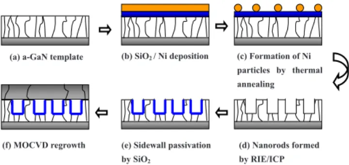
The process of NRELOG is schematically shown in Fig.
1. First, a 1.5-m-thick a-plane GaN layer was grown on r-plane sapphire by metal-organic chemical vapor deposition 共MOCVD兲. Then, a SiO2film with a 200 nm thickness and a
Ni film with a 10 nm thickness were deposited in sequence to act as the etching mask. Subsequently, the thermal annealing treatment was utilized to obtain nanoscale Ni masks. The diameter of the Ni mask is 300–500 nm and the mask density is estimated to be around 6⫻108/cm2as shown in Fig.2共a兲.
The Ni masks exhibit a random distribution with arbitrary geometries. After that, the GaN nanorods were etched through the nanomask openings by reactive ion etching 共RIE兲/inductively coupled plasma etching 共ICP兲 until the height of these nanorods is 0.5 m. The etchants for RIE were SF6 and Ar, and the etchants for ICP etching were Ar, BCl3, and Cl2. Then, the SiO2 films were deposited on the
nanorods. Since the etching rate of RIE is anisotropic 共the vertical etching rate is faster than horizontal etching rate兲, we can control the RIE parameters to remove the SiO2on top of a-plane nanorods and simultaneously leave residual SiO2on
sidewalls of rods, as shown in Fig.2共b兲. We can observe that sidewalls of GaN nanorods are passivated by a 10-nm-thick
a兲Electronic mail: [email protected].
b兲Electronic addresses: [email protected] and
(a) a-GaN template (b) SiO2/ Ni deposition (c) Formation of Ni particles by thermal annealing
(d) Nanorods formed by RIE/ICP (e) Sidewall passivation
by SiO2 (f) MOCVD regrowth
FIG. 1. 共Color online兲 Flowchart of a-plane GaN NRELOG process.
APPLIED PHYSICS LETTERS 94, 251912共2009兲
0003-6951/2009/94共25兲/251912/3/$25.00 94, 251912-1 © 2009 American Institute of Physics
This article is copyrighted as indicated in the article. Reuse of AIP content is subject to the terms at: http://scitation.aip.org/termsconditions. Downloaded to IP: 140.113.38.11 On: Wed, 30 Apr 2014 15:01:03
SiO2 film and the top of nanorods exhibit the flat a-plane
surface. Because the nanorods were fabricated via Ni masks, the shape and homogeneities of nanorods was similar to that of Ni masks. Finally, the GaN regrowth was performed on the nanorod template by MOCVD.
Figures2共c兲and2共d兲show the scanning electron micros-copy 共SEM兲 images of initial regrowth on a-plane GaN na-norods in 45° and 90° angle of view, respectively. The inset of Fig. 2共c兲 illustrates a GaN seed grown on the a-plane nanorod. Because of the sidewall passivation, the GaN re-growth along the side facets of rods was suppressed and GaN seeds only deposit on the top of nanorods. Since the growth rate in the Ga face 共+c direction兲 was tenfold magnitude higher than that in N face 共−c direction兲,5 the Ga face be-came the arrowlike shape. The morphology of the N face became a half of hexagon and maintained mirrorlike flatness as shown in Fig.2共d兲. As a result, the shape of the GaN seed was similar to that of the lying hexagonal pyramid. These GaN seeds combined with each other and finally became a fully coalesced GaN film. Figure 2共e兲 shows the cross-sectional SEM image of the fully coalesced GaN film. The NRELOG coalesced process can be completed within the thickness of 10 m in comparison to the fully coalescence
thickness of over 20– 40 m obtained in previous LEO techniques. Figure 2共f兲exhibits the magnified picture of the black circular dotted line in Fig. 2共e兲. We observed that the NRELOG epilayer was suspended on the GaN nanorods due to the sidewall passivation by SiO2. Figures 2共g兲 and 2共h兲
show the 5 m2atomic force microscopy共AFM兲 images of
the as-grown sample and the NRELOG sample, respectively. These two samples were grown under the same growth con-ditions 共the growth temperature, pressure, and V/III ratio were 1180 ° C, 200 mbar, and 800–900, respectively兲. Com-pared with the as-grown sample, the NRELOG sample ap-parently had the superior surface quality and less surface pits, which are believed to be originated from the TD termi-nations with the surface.2 Therefore, the less surface pits show the possibility of dislocation reduction. The rms rough-ness of the NRELOG sample was approximately 1.9 nm, which was smaller than that of the as-grown sample共nearly 4.1 nm兲.
A high-resolution x-ray diffractometer共Bede D1兲 with a Cu target was employed to investigate the crystalline quality of GaN epilayers. All data are collected at 40 KV, 50 mA using a line focus x-ray source with 10 arc sec per step. The omega x-ray rocking curves共XRCs兲 on-axis 共112¯0兲 and off-axis 共11¯01兲 reflections for the as-grown 共1.5/10 m thick-ness兲 and NRELOG a-plane GaN samples were measured as shown in Figs.3共a兲and3共b兲, respectively. It revealed that the on- and off-axis full width at half maximum共FWHM兲 were narrowed with increasing layer thickness due to the inclina-tion in bulk epitaxial GaN growth. Moreover, the XRC FWHMs of the NRELOG sample on-axis and off-axis reflec-tions were further reduced from 903 to 430 arc sec and from 1821 to 1148 arc sec with respect to the as-grown sample with 10 m thickness. In comparison with the FWHMs of the as-grown and NRELOG samples grown to similar thick-ness, it is evident that the crystal quality of the a-plane GaN epilayer indeed could be improved with the NRELOG tech-nique. On the basis of previous literature,4–7 the on-axis FWHM value of NRELOG samples 共430 arc sec兲 is even narrower than that of the SiNxnanomask LEO共900 arc sec兲/
single-step ELOG sample 共612 arc sec兲 and is comparable to that of either SALE or sidewall LEO sample 共⬃324 arc sec兲.
The typical bright-field cross-sectional transmission electron microscopy 共TEM兲 image near 关11¯00兴 zone axis of the NRELOG sample is shown in Fig. 4共a兲 共acceleration voltage= 120 kV兲. Inset presents the corresponding electron diffraction pattern. The yellow dotted lines represent the con-tour of GaN nanorods. Regions I and II show the nanorod template and the GaN regrowth epilayer, respectively. From
500nm Ni masks
Sidewall SiO2film a-plane GaN nanorod
500 nm +C -C +C -C GaN seed 10.0 nm 20.0 nm 0.0 nm N-face of GaN
(c)
2μm(e)
(a)
(b)
(g)
(h)
SNRELOG layer Nanorods GaN template 1μm(d)
Nanorods(f)
10μm 1μm 2μm 2μmFIG. 2. 共Color online兲 SEM images of 共a兲 nanoscale Ni masks. 共b兲 Fabri-cated GaN nanorods.共c兲 Initial MOCVD regrowth on a-plane GaN nano-rods in 45° angle of view and共d兲 in 90° angle of view, and 共e兲 fully coa-lesced a-plane GaN films in cross-sectional view.共f兲 The magnified picture of the black circular dotted line in共e兲. 共g兲 and 共h兲 5 m2AFM images of
the as-grown sample and the NRELOG sample, respectively.
FIG. 3. 共Color online兲 XRCs 共a兲 on-axis共112¯0兲 reflections and 共b兲 off-axis 共11¯01兲 reflections for as-grown 共1.5/10 m兲 and NRELOG a-plane GaN films.
251912-2 Ling et al. Appl. Phys. Lett. 94, 251912共2009兲
This article is copyrighted as indicated in the article. Reuse of AIP content is subject to the terms at: http://scitation.aip.org/termsconditions. Downloaded to IP: 140.113.38.11 On: Wed, 30 Apr 2014 15:01:03
the TEM image, it is obvious that TD density in region II is much lower than that in region I. The mechanism of TD reduction by NRELOG is similar to the previous LEO methods.4–7 The GaN seeds initially grown on the a-plane nanorods are the windows, and the subsequent lateral over-grown GaN are the wings. We can observe that the disloca-tion lines from region I penetrated into region II via the nanorods共windows兲. In contrast, the GaN wing between two nanorods was essentially free of dislocations. The average TD density in region II was estimated to be 3.5⫻108 cm−2, which was about two orders of magnitude lower than that in region I共3⫻1010 cm−2兲. In addition, the stacking fault 共SF兲
was observed from the plan-view TEM image near 关112¯0兴 zone axis as shown in Fig. 4共b兲. The SF density was esti-mated to be 2⫻105 cm−1, which was decreased by a factor of 2–3 compared to that of as-grown sample. We believe that the TD and SF density could be further decreased while the optimization of nanorod parameter is performed.
Temperature-dependent photoluminescence 共PL兲 was utilized to investigate the quantum efficiency of the grown samples. In general, the temperature-induced quenching of luminescence involves the thermal activation of excitons to nonradiative defect states.8In other words, a slower intensity decline with the temperature increasing means a lower defect density in the grown sample. The normalized inte-grated PL intensity ratio obtained at 20 and 300 K 关IPL共300 K兲/IPL共20 K兲兴 could represent the IQE of the GaN
samples. Figure4共c兲shows the normalized integrated PL in-tensity of GaN emission as a function of 1000/T for the as-grown sample and the NRELOG sample. The IQE ob-tained from关IPL共300 K兲/IPL共20 K兲兴 value for the NRELOG
GaN has a 3.4-fold increase compared to that of the as-grown GaN. The reduction in the TD density in case of NRELOG samples as compared to as-grown samples can contribute to the enhancement in the quantum efficiency and thermal activation energy.9
In conclusion, we have grown high-quality and fully coalesced a-plane GaN films by using NRELOG. The fully coalesced thickness 共10 m兲 of NRELOG sample was
de-creased by a factor of 2–4 with respect to the previous re-ported LEO techniques, such as ELOG, SALE, and sidewall LEO.5–7 According to the result of TEM, the average TD density can be apparently reduced from 3⫻1010 to ⬃3
⫻108 cm−2. The XRC FWHMs on- and off-axis reflections
were decreased from 1308 to 430 arc sec and from 2420 to 1148 arc sec, respectively, demonstrating the strain mitiga-tion and the improvement of the crystal quality by NRE-LOG. Additionally, the temperature-dependent PL result showed the 3.4-fold increase in IQE compared with the as-grown GaN, which could be attributed to the TD density reduction. A series of experiments demonstrated the feasibil-ity of using NRELOG technique to achieve the TD reduc-tion, crystal quality improvement and the enhancement in luminescence performance in a-plane GaN.
This work was supported by the Ministry of Economic Affairs of the Republic of China共MOEA兲 and in part by the National Science Council of Taiwan under Contract Nos. NSC 96-2221-E009-094-MY3. The Grant No. of the MOEA project was 7301XS1G20 for the nonpolar GaN epitaxy and MOVPE part.
1T. Takeuchi, S. Sota, M. Katsuragawa, M. Komori, H. Takeuchi, H.
Amano, and I. Akasaki,Jpn. J. Appl. Phys., Part 2 36, L382共1997兲.
2M. D. Craven, S. H. Lim, F. Wu, J. S. Speck, and S. P. DenBaars,Appl. Phys. Lett. 81, 469共2002兲.
3A. Chakraborty, B. A. Haskell, S. Keller, J. S. Speck, S. P. DenBaars, S.
Nakamura, and U. K. Mishra,Appl. Phys. Lett. 85, 5143共2004兲.
4A. Chakraborty, K. C. Kim, F. Wu, J. S. Speck, S. P. DenBaars, and U. K.
Mishra,Appl. Phys. Lett. 89, 041903共2006兲.
5B. A. Haskell, F. Wu, M. D. Craven, S. Matsuda, P. T. Fini, T. Fujii, K.
Fujito, S. P. DenBaars, J. S. Speck, and S. Nakamura,Appl. Phys. Lett.
83, 644共2003兲.
6C. Chen, J. Zhang, J. Yang, V. Adivarahan, S. Rai, S. Wu, H. Wang, W.
Sun, M. Su, Z. Gong, E. Kuokstis, M. Gaevski, and M. A. Khan,Jpn. J. Appl. Phys., Part 2 42, L818共2003兲.
7B. Imer, F. Wu, S. P. DenBaars, and J. S. Speck, Appl. Phys. Lett. 88,
061908共2006兲.
8Y.-h. Wu, K. Arai, and T. Yao,Phys. Rev. B 53, R10485共1996兲. 9J. S. Hwang, A. Gokarna, and Y,-H. Choa,J. Appl. Phys. 102, 013508
共2007兲. 500 nm Ⅰ Ⅰ Ⅱ Ⅱ 500 nm Ⅰ Ⅰ Ⅱ Ⅱ [1120] [0001] [1100] [1120] [0001] [1100] (a) 500 nm [1100] [1120] [0001] [1120] [1100] [0001] (b) 200 nm (a) 0 10 20 30 40 50 1 N o rm a li z e d P L inte n sity (a .u .) 1000/T (K-1) NRELOG a-plane GaN As-grown a-plane GaN (c)
FIG. 4. 共Color online兲 共a兲 Typical bright-field cross-sectional TEM image near 关11¯00兴 zone axis of the NRELOG sample. Inset shows the corresponding electron diffraction pattern. The yellow dotted lines represent the contour of GaN nanorods.共b兲 The plan-view TEM image near 关112¯0兴 zone axis of the NRELOG sample.共c兲 Arrhenius plots of the normalized integrated PL intensity over the temperature range of 20–300 K for the as-grown GaN and NRELOG GaN.
251912-3 Ling et al. Appl. Phys. Lett. 94, 251912共2009兲
This article is copyrighted as indicated in the article. Reuse of AIP content is subject to the terms at: http://scitation.aip.org/termsconditions. Downloaded to IP: 140.113.38.11 On: Wed, 30 Apr 2014 15:01:03