A Novel Memory Architecture for Video Signal Processor
Jen-Sheng Hung. Chia-Hsing Lw and Chein-Wel Jen National Chiao lung University, Institute of ElectronicsHsinchu. Taiwan. ROC
ABSTRACT
An on-chip memory architecture for video signal processor (VSP) is proposed. This memory structure is a
two-level design for the different data locality in video applications. The upper level --Memory A provides enough storage capacity to reduce the impact on the limitation of chip I/O bandwidth, and the lower level --Memory
B provides enough data parallelism and flexibility to meet the requirements of multiple
re-configurable pipeline function units in a single VSP chip. The needed memory size is decided by the memory usage analysis for video algorithms and the number of function units.Both levels of memory adopted a dual-port memory scheme to sustain the simultaneous read and write operations. Especially, Memory B uses niultiple one-read-one-write memory baaks to emulate the real
multi-port memory. Therefore, one can change the configuration of Memory B to several sets of memories with variable read/write ports by adjusting the bus switches. Then the numbers of read ports and write ports in
proposed memory can meet requirement ofdata flow patterns in different video coding algorithms.
We have finished the design of a prototype memory design using 1.2-ini SPDM SRAM technology and will fabricate it through TSMC, in Taiwan.
1. INTRODUCTION
As the rapid development of VLSI technology, it is possible to embed multiple processing units in a single chip to solve computation-intensive problems such as the diverse complex video coding algorithms. Especially. the same data are often repeatedly used in most video applications like motion estimation and DCT, etc. Therefore, parallel processing scheme, such as a video signal processor (VSP) with multiple processing units working concurrently, is very suitable for the real-time video applications. However, the chip I/O bandwidth will limit the utilization of processing units if it cannot meet with the computation rate. On facing the fact, an on-chip storage with adequate size and structure is heavily used as an important embedded element in VSP to meet the requirement ofnuiltiple processing units and release the chip from high I/O bandwidth"23 demand.
Capacity and parallelism are the major considerations for on-chip memory structure in order to reduce the impact on the limitation of chip I/O bandwidth and to meet the access demands of multiple re-configurable pipeline function units in a single chip VSP. The on-chip memory design in VSPs designed by Yamauchi4, Murakami5, and Tamitani6, which adopted dual-port scheme, may meet the capacity requirements; however, it is difficult for multiple processing units to access the data in the same location without introducing processor stalls if VSP doesn't provide complex routing and addressing scheme. On the other hand. a multi-port memory structure could may be a candidate to provide enough parallelism. However, as the number of ports increases, the area growths make it is hard to provide enough storage capacity. Therefore, an on-chip memory structure should be able to make trade-offhetveen size and parallelism for on-chip memory.
In this paper, we proposed a two-level memory structure to fit the considerations of on-chip memory. The upper level --MemoryA provides enough storage capacity to reduce the impact on the limitation of chip I/O
bandwidth, and the lower level --Memory B provides enough data parallelism to meet the requirements of multiple re-configurable pipeline function units in a single VSP chip. In Section 2, we will analyze the source
coding algorithms to decide the required size of on-chip memory. In Section 3, We will discuss the
implementation difficulty of real multi-port memory and present a more feasible and flexible alternative. We will also describe the proposed two-level memory architecture. A prototype design of 3.5-kbyte that applied the two-level concept will be presented in Section 4. The conclusions are summarized in Section 52. ANALYSIS OF MEMORY SIZE IN VIDEO CODING ALGORITHMS
--BLOCK
MATCHING
Because of the random access characteristic indiversealgorithms, and the relatively huge data amount in a
search block, the size of on-chip memory is actually decided by the requirement of motion vector detection. We here compute the size of required on-chip memory for the motion vector calculation under different constraints of I/O bandwidth, and study the impact of memory size one the realization of algorithms.
Assume the maximum motion vector displacement is D, and a macroblock has an edge EMB. To simplify this calculation, here we choose the fundamental memory unit as a size of S —(2D+EMB) EMB, which is one row or one column of macroblocks in a search block.
First, let we consider the case that on-chip memory size is smaller than a search block. In the simplest case where the sequence of block matching is predicable as that in full-search algorithm, the data to be loaded vhile searching for the current motion vector is
(2D +EMB)2 - N*S= (2D
-
(N1)*EMB)*(2D+EMB) (1)Here we assume the memory size is a multiple of S. that is, N*S. The term (2D +EMB)2 isthe size of a
search block. Fig. 1 shows the relation of on-chip memory size and the required input pixels for each motion vector calculation while the size of on-chip memory is less than that of search blocks.
With a fixed macroblock size, from (1) we could find that there are two ways to reduce the requisite data
bandwidth: to lower the support of displacement D or to increase the on-chip memory size. However, to
increase N is not definitely able to reduce I/O bandwidth. because most of the algorithms do not personate a predicable data sequence in block matching. While searching for a motion vector, data in a search block may be repeatedly read from outside because it is used by different on-matching macroblocks across the margin of
loaded and non-loaded data. Besides, it takes time to load the following search block if it depends on the
current result ofblock niatching.
To reduce D may be a more reasonable approach since D actually dominates the outcome of (1). With
smaller D, the same iuemory size can cover more ofa search block. Fig.2 shows the relation between D and the corresponding search block size.
On the other hand, in the case that oii-chip memory is larger than a search block, it is possible to store
used pixels that will be again accessed later. Fig.3 shows the relation ofthe on-chip memory size (larger than a
search block) and the required input pixels with a frame I 125 lines, macroblock size 16 by 16, and D=64.
Furthermore, if there is extra memory capacity available, processor could also load the data belonging to the
next search block that is not used in the current motion vector calculation to avoid unnecessary stall. This
further storage requirement is EM.B *(2D + EMB)and is equal to (the required input data bandwidth for
motion vector calculation) K: K is the nuiiiber of clocks to find a motion vector.
On the basis of this consideration, a reasonable on-chip memory for motion vector calculation of divergent
algorithms with D —64and B = 16would be
(2D +EMB)2 + EN'tB (2D+EMB)=22.5K (bytes). (2)
From the above discussion. we see that to keep a nrnderate I/O bandwidth, there is a lower bound for the size of chip memory in order to facilitate the implementation of diverse algorithms. yet the increase of on-chip memory size inay not proportionally reduce the I/O bandwidth when it excesses a constant. because of the
limitation of data access sequence.
3. MEMORY ORGANIZATiON
3.1 TheIdealMemory Model and The Difficulty of RealizationWhen several processing units are embedded in a single chip VSP. an ideal on-chip memory should also provide enough parallelism for the concurrent data requirements of multiple processing units to prevent processor stall, in addition to have enough capacity. Derived from the frequently met block operations and different data locality in video processing, we proposed a two-level memory structure: The upper level
--Memory-B represents a moving window capable of offering large data parallelism. This memory structure is well suitable for blocking-matching algorithm. Furthermore, there is also no need of extra routing mechanism
to perform bit-reverse, butterfly, or transpose if memory B has sufficient read ports and write ports. Thus,
algorithms like DCT, FFT, and filtering are also well performed.
It seems that multi-port RAMs are necessary to support heavy data consumption rate in B and to keep
enough bandwidth between both levels. However, problems involved in the realization of multi-port memory are: (i) To concurrently enable different cells of a memory bank, it must duplicate the decoder, and therefore the word lines as well. (ii) It must duplicate both bit lines and sense amplifiers while the number of read ports increases. (iii) Each cell should have adequate driving capability to cope with the worst case situation, which occurs at a time that one cell read by all ports simultaneously'. (iv) There needs at least one more transistor as control for each additional port.
Since both word lines and bit lines are duplicated, the increase of chip area owed to these two parts is
expected to be 0(N2), where N is the number of ports. That is, the area cost will become high if the required number of ports is large, which in turn worsen the cycle time of memory.
3.2 TheProposedMemory
On the basis of the above discussion of the difficulty in the realization of real multi-port memory, we use one-read-one-write memory banks to emulate such memory. The basic methodology is to duplicate all possibly used
items into the corresponding memory banks. Fig. 4 and Fig. 5show the applications of this architecture in
butterfly-style memory access and blocki ug-matchi ng, respectively.
In Fig. 4, data xl through x4 are copied into all eight bank-B's, and the butterfly style operation can be
finished without the need of special routing.
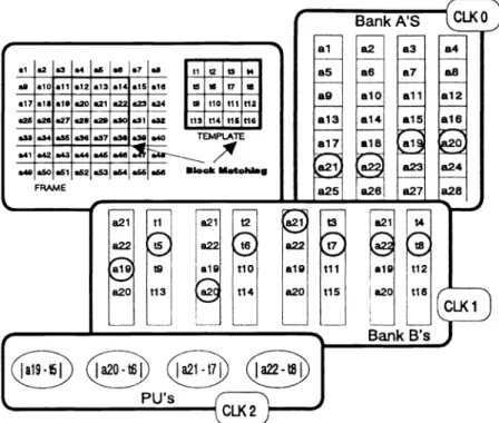
In Fig. 5 we are going to match 2 blocks (This procedure may be occurred quite frequently in vector quantization or motion vector calculation). At clock 0, the frame pixels are loaded into bank-A's, which is
constituted offour one-read-one-vrite memory banks (al, a5, a9, a13, ...inone bank, a2, a6, alO, ...inanother bank, and so on) and the template pixels from U to t16 are scattered into four of the eight bank-B's. Assume we are now calculating the absolute-difference values of the second row of both blocks: at clock 1 pixel a19 to
a22 are duplicated into the other four of bank-B's, and four absolute-difference operations can be executed
simultaneously at the following clock (clock 2).
The proposed memory for four functional units is shown in Fig.6. Tvo storage levels --MemoryA and Memory B constitute this niemory. Each level consists of multiple one-read-one-write memory banks that are organized to be a quit flexible multi-port structure. The Memory A, which provides enough storage capacity,
behaves as the input buffer memory. On the other hand, the memory B, which provides enough data
parallelism, can offer up to sixteen 8-bit parallel read ports alone with four 16-bit parallel write ports for four function units. Those two levels are communicated by four 32b buses to support the computation rate. Several bus switches are used to connect-disconnect different buses for more flexibility. Thus, through different setting ofbus switches, the Memory B can be further divided into two independent 8-read-2-write or four independent 4-read-l-write memories vith equal size, and each has the same size as the original 16-read-4-write structure. This memory can be organized as a 16-one-read-4-one-svrite structure, too, and the total size is sixteen times the 16-read-port-4-write-port case.
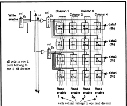
Fig.7 shows the details of one memory bank B. SEL2's decide the data writing pattern of bank-B's.
Table. 1 lists the enable line(s) chosen by SEL2. By way of proper writing sequence as well as the setting of SELl's and SEL2's. this memory can be organized with fair elasticity. Table.2 lists some ofthe examples.
Switches in Fig. 6 decide the break or concatenation ofbuses, which can divide bank B's up to four groups.
Data fron bank A's. direct input or function units (FUs) are written to bank B's according to the setting of SELl's and SEL2s. If the configuration is chosen that each input data will appear in all selected N read columns, those N columns compose an N-read-M-write memory, where M may vary from one to four
depending on how those columns are arranged.
The memory we proposed can be used for video signal processor with embedded multiple re-configurable pipeline function units to fit data flow patterns in algorithms. We may choose the (read ports)/(write ports) ratio and data precision according to the average input/output ratio and accuracy requirement. Compared with
the memory structure that uses shared bus's structure and explicitly routing mechanism4, the niemon we
proposed is more changeable under different considerations. There is also no need of explicit output buffer
memory'6 and of extra routing mechanism because of the flexibility of Memory-B. The area growth ratio of this memory structure is 0(N) instead ofO(N2) like real multi-port memory.
4. A PROTOTYPE MEMORY DESIGN
The memory structure we proposed has been designed and simulated with 1 .2 jtSPDMtechnology and will be
fabricated by TSMC, in Taiwan. The structure consists of eight-transistor, two-port, static-RAM cells and occupies 7.2 x 9.3 mm2 chip. With the limitation in die size, we only implemented the half the required
memory size for D : 16and B = 16.that is, 1.5K (bytes) for Memory-A and 2K (bytes) for Memory-B. Each Memory-B bank consists of sixteen l6bytes' sub-banks like Fig. 7. However, we place those sub-banks to be a
sixteen-by-one linear array instead of a four-by-four mesh in actual layout so that we could eliminate unnecessary global routing and to share the write word line. The penalty of that is the need of additional
column decoders and more heavy word line loading. By separating the read-write circuitry, the required
one-read-one-write memory banks can be implemented. The simulation results using SPICE is shown in Fig.8,
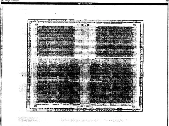
where four cycles: Write 'I'. Read '1'. Write '0'. Read '0' are performed. The layout of the core circuit is shown in Fig.9.
5. CONCLUSION
Observing the requirement in the size and parallelism of on-chip memory in video signal processor with
multiple functional units, 'e proposed a two-level memory with multiple banks for those applications and used duplication of data to emulate the real hard-to-implemented multi-port storage. The memoty organizes one-read-one-write dual port modules to configure a quit flexible structure that can fully support VSP application.
The conflict of capacity and flexibility shown in traditional on-chip memory design is moderated by the
proposed two-level scheme.
A prototype 3.5-kbyte memory with two-level structure was designed and will be fabricated with 1.2-rim CMOS technology.
6. REFERENCES
1. R. D. Jolly, "A 9-ns, 1.4-Gigabyte/s. 17-Ported CMOS Register File." IEEE JSSC, Vol. 26, NO. 10, pp.1407-1412. Oct. 1991.
2 K-I. Endo T. Matsuniura, J. Yamada, "A Flexible Multiport RAM Compiler for Data Path." IEEE
Jssc, Vol. 26, NO. :3, pp. 343-348, Mar. 1991.
3. K-I. Endo, T. Mastumura. J. Yamada. "Pipelined, Time-Sharing Access Technique for an Integrated Multiport Memory." IEEEJSSC, Vol. 26. NO 4. pp. 549-554, Apr. 1991.
4. H. Yarnauchi, Y. Tashiro, T Minanu. Y. Suzuki, "Architecture and Implementation of a Highly
Parallel Single-Chip Video DSP." IEEE Trans. Circuit and sv.v(e/1lp)rJic/eo Technology, Vol. 2, NO. 2, pp. 207-220, Mar. 1992.
5. T. Murakami, K. Kamizawa, M. Kameyama, S.I. Nakagawa, "A DSP Architectural Design for Low
Bit-Rate Motion Video Codec." IEEE Trans. Circuit.Sv.vt.,vol. 36, NO. 10, pp. 1267-1274, Oct. 1989.
6. I. Tanutani, H. Harasaki, T. Nishutani. Y. Endo, "A Real-Time HDTV Signal Processor: HD-VSP."
IEEE Trans. Circuitand SYSte111.Ir I'idea TL'chnulogv, vol. 1, NO. 1, pp. 35-41 Mar. 1991.
7. H. B. Bakoglu, "Circuit. Interconnections, and Packaging for VLSI". Chap. 4, Addison-Wesley, 1990. 8. J. S. Hung, "A Datapath Design For Video Signal Processor". Master thesis. Institute of Electronics. NCTU, 1992.
274 ISPIE Vol. 1976 High-Definition Video (1993) 25000 20000 15000 Bytes 10000 5000 0 1 2 3 4 5 6 7 8 9 N
Figure 1. Input data vs.on-chipmemory size for on-hip size<search block size.
On-chip Memory Size (Byte
4 8 1216202428323640444852566064
D: Displacement (Pixek
Input Data (Bytes)
Figure 3. Input data vs. on-chip memory sizeforoti-hip size>search block size.
x2Lx2
X3 X3
L\
ii1
Xl op X4 Bank B'sx2H2
X3 X3
X4
X4 op XlFigure 4. Butterfly-style memory access 2500 2000 1500 1000 500 0
I
15 --Di[______
0 20000 40000 6000080000 100000 120000 140000 ló0000
On-chipMemory Size (Bytes)
Xl X2 X3 X4
Using Bank-B's to realize special routing such as Butterfly or Bit-reverse
XlopX4 X3opX2 X2opX3 X4opXl X2
X2!
X3 X3
X3)X3
X4 X4
X4 X4
X2opX3 X3opX2276 /SPIE Vol. 1976 High-Definition Video (1993)
Figure 5. Blocking Matching for ME or VQ
Single B A N K As 32b l6b r"ii Muxs
iJ*l6b.
l6 16b IJux B A N K BsFigure 6. The Proposed Memory Organization
e read co1um
ItI
uI1
tki1f4
1tT1LiI
Read Read Read Read enable enable enable enable
1
2
4eachcolumn belongs to one read decoder
I1 GENEROT(O IROPI SPICE.1.MG BY MG!C'S SPICE GENERTOR
29-SEP92 2147 3 : MEM ro V 40 .
\ .— WWL
/ EWteWordLtne MONt ro 4.0 — RWL::
_
Ij
I:ttne
N 2 0 - Input U ..I .. . . Mr P:
: r
_____I -
I
0 50 ON 100 ON 150 ON 200.ON 0. T1ME(LIN) 240.ONFigure8. SPICE simulation results --Fourcycles: Write 1, Read 1, Write 0, Read 0 areshownrespectively
Write Sd enable Colurrvi 1 Column 3 H se 2b Column 2 Comn 4
DML1
datal (8b).!:I:I II I
sel Ii1Ji LJ.l
]ji1ll:1
I±
I Iall cells in one B.
Bank beloong to one 4—bit decoder
LJ.1
V L (8b)riI
r
data4
(8b)column (s) selected 1 2 3 4
SEL2=OO
0
0
0
0
SEL2=O1
Q
Q
SEL2=lO
Q
QSEL2=l1
Q
Table. 1 The enabled column(s) in a B memory hank corresponding to different control signals of SEL2
setting sequence of SEL2
resulted data in columns
column! coluinn2 column3 column4
OO—*O1---—>1O-—>11 data4 data3 data2
datal
00—>01 data2 data2 datal
datal
00—> 10 data2 data I data2 data 1
00—> 11 data2 data 1 data 1 data 1
Tahle.2 Final results in the four columns of a B memory hank while control signal of SEL2 is changed sequentially, and has a duration 1 clock.
278ISPIE Vol. 1976 High-Definition Video (1993)