The increase of resistance-capacitance (RC) time delays resulting from the smaller feature size devices fabricated on large dies, longer transmission lines, and more closely spaced interconnects will con-tinue to bring further challenges in the semiconductor industry. Device integrated with lower dielectric constant material and lower resistance Cu film is capable of improving its performance and reducing the interconnection delay. Currently, Cu and hydrogen silsesquioxane (HSQ) are the leading candidates for metal and dielectric, respectively. However, the diffusivity of Cu in HSQ is rather high. The degradation and transport of copper is through its oxidation and diffusion/migration of ions. Cu interconnects need a barrier layer around them to prevent the diffusion into the interlayer dielectric. The diffusion of Cu will cause the dielectric to fail; name-ly, it can lead to a significant increase in leakage current. The goal of this work is to reduce the diffusion of Cu into the dielectric.
The HSQ has the following characteristics: carbon free, reflowa-bility, low dielectric constant, and a good gap-filling capability. If we want to replace the commonly used SiO2 with the organic low-k material, a number of process compatibility and reliability issues have to be addressed. Among them, the most important ones include electrical characteristics, thermal properties, and moisture absorp-tion. Various materials have been studied as diffusion barriers be-tween Cu and SiO2interface. The conductive barriers Ta, Ti, W, and their alloys such as TiN, TiW, WN, TaSi, and TaSiN were investi-gated successfully.1,2However, the barrier metal-free structure can specially reduce the resistance in fine patterns.3,4An excellent barri-er capability is obtained by forming a thin barribarri-er laybarri-er of SiON on the surface of SiOF film.3 Gardnes et al.5 also demonstrated that using a thin SiN film as a barrier layer was better than using a refrac-tory metal in lowering device RC delay time.
Flowable oxide (FOx-16), a type of spin-on HSQ, is a low-k material used in this study. It is shown that the H2annealing and H2 plasma treatment of low-k materials are capable of reducing the device’s leakage current.6However, their barrier capability against Cu is still unsatisfactory. A thin nitride film formed on the surface of HSQ by NH3plasma treatment can result in very successful results. In other words, the capability of suppressing Cu using an additional plasma treatment is much better than the as-cured sample.
Experimental
A dilute fluid of HSQ (FOx-16:FOx-1 5 1:3) was spun on (100) 4-7 V-cm p-type Si wafers. Its thickness was approximately 100 nm after curing at 3508C for 60 min. The process steps used in this study are listed as follows:
1. An 100 nm HSQ was spun on the Si substrate.
2. HSQ was treated with a NH3or H2plasma by plasma enhanc-ed chemical vapor deposition (PECVD) technique. The substrate tem-perature was 3008C, the pressure was 40 Pa, the flow rate for NH3or H2was 300 sccm, and the RF power was 300 W.
3. A Cu film of 200 nm was deposited on the different samples by sputtering and then formed a metal oxide semiconductor (MOS) capacitor structure.
Several different measurement techniques were used to measure the various properties of all as-deposited and annealed samples. Fourier transform infrared (FTIR) spectra can help us understand the molecular structure of the material. The atomic concentrations of Cu ion in HSQ film were examined by secondary ion mass spectrome-try (SIMS). The percentage of nitrogen in HSQ is measured by X-ray photoelectron spectroscopy (XPS) technique. The dielectric constant was calculated from capacitance-voltage (C-V) plots using MOS structure. The leakage current was measured by precision semiconductor parameter analyzer (HP 4156A).
Results and Discussion
Figures 1a and b show the FTIR spectra of cured FOx-16 after NH3and H2plasma treatment with different exposure times. These figures indicate that the HSQ structure starts to convert to Si-O stretch network structure after its being treated by NH3or H2 plas-ma, i.e., HSQ film becomes denser after plasma treatment. The high density of this HSQ structure implies that it has larger refractive index and dielectric constant. The dielectric constant varies with dif-ferent plasma exposure times as shown in Fig. 2. The initial as-cured value of HSQ is 2.7, and it increases slightly as the exposure time increases. This result agrees with the fact that the HSQ film becomes denser after plasma treatment. The slightly higher dielectric constant implies that the thin nitride film was formed only on the surface of SOG after NH3plasma treatment.
SIMS analysis shows that the thickness of nitride film is about 35 nm on the surface of HSQ after NH3plasma treatment for 10 min as shown in Fig. 3a. The nitride film is the best material to be used as a barrier to guard against the impurity diffusion/migration. Loke
et al.7 showed that Cu1 penetration can be prevented by 75 nm nitride layer. As shown in Fig 3b, the HSQ film demonstrated an obvious improvement after its being treated by NH3 plasma for 10 min. From this figure, we found that copper can diffuse into the as-cured HSQ at 5008C. On the other hand, after NH3plasma treat-ment for 10 min, the HSQ film demonstrated better characteristics than the cured sample. In addition, the Cu depth profile of an as-cured sample is almost the same as the one having a 5008C
anneal-Using NH
3
Plasma Treatment to Improve the Characteristics of
Hydrogen Silsesquioxane for Copper Interconnection Application
Kow-Ming Chang, I-Chung Deng,* Sy-Jer Yeh, and Yao-Pin Tsai
Department of Electronic Engineering and Institute of Electronics, National Chiao Tung University and National Nano Device Laboratory, Hsinchu, Taiwan
Hydrogen silsesquioxane, a material with low dielectric constant, can successfully suppress Cu diffusion without using a barrier metal by implementing a NH3plasma treatment. Lower leakage current and better barrier capability can be achieved by hydrogen silsesquioxane film after NH3plasma treatment. Having been treated with different plasma exposure times, this film can still main-tain its original dielectric constant with few changes. The decrease in leakage current with increasing exposure time can be attrib-uted to the following mechanisms: dielectric film becomes denser, dangling bonds are passivated, nitride film is formed on the hydrogen silsesquioxane, and the bulk damage of hydrogen silsesquioxane is annealed out. A thin layer of nitride formed on the dielectric is the cause for having better capability. The thickness of the nitride layer on hydrogen silsesquioxane is about 35 nm, and it can prevent the Cu diffusion/migration into the underlying dielectric. The role of our nitride film is to act as a passive dif-fusion barrier.
© 2000 The Electrochemical Society. S0013-4651(99)10-093-4. All rights reserved. Manuscript received October 24, 1999.
ing for 60 min. This directly proves that the NH3 plasma-treated HSQ has successfully blocked the Cu diffusion. From XPS analysis, we found a strong peak of N1Sat 398 eV and a weak peak of N1Sat
403.5 eV as shown in Fig. 4. The lower binding energy of N1S is attributed to the electron transfer from Si to nitrogen atom. In other
Figure 1. FTIR spectra of cured HSQ after (a, top) NH3plasma treatment,
(b, bottom) H2plasma treatment for different exposure times.
Figure 2. The variation of dielectric constant after different plasma treatment conditions.
Figure 3. (a, top) SIMS depths profile of as-cured HSQ. (b, bottom) Com-paring the Cu penetrated into HSQ after annealing at 5008C for 60 min.
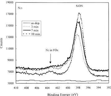
Figure 4. N1SXPS spectra of HSQ after NH3plasma treatment for different
words, the role of our nitride should act as a passive diffusion barri-ers.8,9The passive barrier is considered to be probably the best dif-fusion barrier.10It causes a significant improvement in the dielectric characteristics. Figure 4 shows that the strength of N1Speak increas-es with increasing the plasma treatment time. The percentage of nitrogen atoms in HSQ film also increases with increasing the NH3 plasma treatment time as shown in Table I. The increasing percent-age of nitrogen atoms implies that the barrier effect is improved after longer plasma treatment time. The percentage of nitrogen atoms increases rapidly first and then reaches to a saturation point after a 7 min NH3plasma treatment. The nitrogen concentration only in-creases 2% between 7 and 10 min NH3plasma treatment.
Figure 5a shows the leakage current density of MOS capacitors. A decrease in leakage current after NH3plasma treatment can be observed. The leakage current decreased further with increasing plasma exposure time. This result is similar to the samples after H2 plasma treatment in Fig. 5b. The reasons for reducing the leakage current can be attributed to the following: (i) the HSQ film becomes denser after plasma treatment; (ii) the passivated dangling bonds in the SOG cause a decrease in leakage current with increasing plasma exposure time. Hydrogen being passivated plays a major role of pas-sivation; while the previous work6found an increase in leakage cur-rent after N2plasma treatment; (iii) thin nitride film of 35 nm on the HSQ can effectively block the electrical field which could otherwise induce Cu ion drifting into the HSQ; (iv) the plasma damage is only on the surface of the HSQ film and the damage in the bulk of HSQ film is annealed out during plasma treatment.
Figures 6a and b reveal the leakage current for both as-cured HSQ film and its having been treated by NH3plasma, respectively. In Fig. 6a, the capacitor remained intact up to 4008C annealing for 60 min. This arises from the fact that the damage in HSQ is annealed out after annealing at 4008C comparing with the HSQ at room tem-perature of which it has a higher leakage current. The capacitor suf-fered significant degradation with high leakage current after anneal-ing at 5008C for 60 min. After NH3 plasma treatment shown in
Table I. The composition percentage of the surface of FOx with NH3plasma treatment for different times.
Element O 1S N1S C1S Si2P Time (%) (%) (%) (%) No plasma 47.066 10111. 19.377 43.557 13 min 39.214 12.825 13.435 34.526 17 min 30.423 21.369 12.117 34.241 10 min 27.006 23.182 14.099 35.713
Figure 5. The leakage current density of HSQ after (a, top) NH3plasma
treatment, (b, bottom) H2plasma treatment for different exposure times.
Figure 6. The leakage current density of (a, top) as-cured HSQ and (b, bot-tom) NH3plasma-treated HSQ after annealing at 400 and 5008C for 60 min.
Fig. 6b, the leakage current level is of three orders lower than those of as-cured samples at 1 MV/cm electric field. Even after annealing at 5008C for 60 min the leakage current density remains almost the same as the as-treated samples.
Figure 7a shows the breakdown electric field (EBD) distribution of the samples with Cu gate after NH3and H2plasma treatments. HSQ shows a great improvement of breakdown voltage after NH3plasma treatment. We also measured the electric field of the Al gate as shown in Fig 7b. In this case, all of the samples show the same level of breakdown electric field. As the electrode was replaced by Cu, the as-cured sample demonstrated significant degradation. Therefore, Cu is expected to be a major cause of leakage current. The formation of a nitride film on the surface of SOG results in a higher breakdown volt-age and better barrier capability.
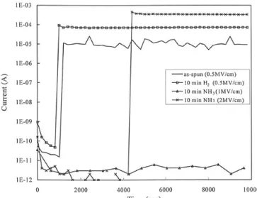
The time to failure (TTF) stress can be used as an indicator to examine the barrier quality. The effect of electric field on copper transport was conducted when the temperature was measured at 1508C. As shown in Fig. 8, the initial decrease in the leakage current is similar to the samples of Cu on oxide or nitride.11,12This decrease in leakage current is due to the injection of mobile ions of Cu into the dielectric. The injection of ions leads to the charge buildup in the dielectric and to oppose further injection. It can be seen that the
leak-age current reduces continuously until it balances with the electron injection from the back-side electrode. In Fig. 8, it was found that the SOG sample with a NH3plasma treatment shows a better integri-ty than the as-cured one after TTF stress test. After applying four times the magnitude of the electric field to the NH3plasma-treated sample, its TTF time is still much longer than those of the as-cured and H2 plasma-treated ones. Finally, at the breakdown stage, the NH3plasma-treated sample shows an abrupt breakdown without a gradual increase in leakage current, which is similar to oxynitride in the other reports.5The “self-healing” phenomena (the leakage cur-rent spikes up and down) are sometimes observed in TTF testing. These phenomena are due to the nonuniform diffusion of copper.11 Based on the above data, the NH3plasma treatment is an excellent method for improving the quality of HSQ.
Conclusion
NH3plasma treatment provides an efficient method for improv-ing the quality of FOx-16, a flowable low-k material. After NH3 plasma treatment, the leakage current shows three orders of magni-tude lower than that of as-cured sample at an electric field of 1 MV/cm. We have found that FOx-16 has capabilities for prevent-ing Cu diffusion after its beprevent-ing treated by NH3plasma. This was due to a 35 nm nitride film formed on the HSQ surface and the overall dielectric constant was not changed. This nitride film offers a dra-matic improvement in terms of barrier characteristics. After anneal-ing in NH3ambient at 5008C for 1 h, no increase in leakage current was observed in the Cu/HSQ/Si structure. The function of nitride film acts as passive diffusion barriers. This thin nitride film can also improve the breakdown voltage of HSQ. As the experimental results indicate, the NH3 plasma treatment is an excellent approach for improving the characteristics of HSQ.
Acknowledgments
This work is supported by the National Science Council under grant NSC88-2215-E-009-046.
National Chio Tung University assisted in meeting the publication costs of this article.
Reference
1. Y. S. Diamand, A. Dehhia, D. Hofstetter, and W. G. Goldham, in Proceedings of the VLSI Multilevel Interconnection Conference, VMIC, p. 109 (1991).
2. S. Hirao, M. Satake, H. Kamada, M. Sekiguchi, T. Tamaki, and S. Mayumi, in Symposium on VLSI Technology, Digest of Technical Papers, p. 57 (1997). 3. K. Mikagi, H. Ishikawa, T. Usami, M. Suzuki, K. Inoue, N. Oda, S. Chikaki, I.
Sakai, and T. Kikkawa, Tech. Dig. Int. Electron Devices Mtg., p. 365 (1996). 4. G. M. Adema, L. T. Hwang, G. A. Rinne, and I. Turlik, IEEE Trans. Comp.,
Hybrids, Manuf. Tech., 16, 53 (1993).
Figure 7. Weibull plot of (a, top) Cu/HSQ/Si and (b, bottom) Al/HSQ/Si structures’ breakdown electric field (EBD) distribution after different plasma
treatment conditions.
Figure 8. Influence of time to failure of Cu/HSQ/Si structure after different plasma treatment conditions.
5. D. S. Gardner, J. Onuki, K. Kudoo, Y. Misawa, and Q. T. Vu, Thin Solid Films, 262, 104 (1995).
6. P. T. Liu, T. C. Chang, S. M. Sze, F. M. Pan, Y. J. Mei, W. F. Wu, M. S. Tsai, B. T. Dai, C. Y. Chang, F. Y. Shih, and H. D. Huang, Thin Solid Films, 332, 345 (1998). 7. A. L. S. Loke, J. T. Wetzel, C. Ryu, W. J. Lee, and S. S. Wong, in Symposium on
VLSI Technology, Digest of Technical Papers, p. 26 (1998). 8. M-A. Nicolet and M. Bartur, J. Vac. Sci. Technol., 19, 786 (1981).
9. M. Nagai and K. Kishida, Appl. Surf. Sci., 70/71, 759 (1993).
10. S. Wolf, in Silicon Processing for the VLSI Era, Vol. 2, p. 123, Lattice Press, Sun-set Beach, CA (1990).
11. G. Raghavan, C. Chiang, P. B. Ander, S. M. Tzeng, R. Villasol, G. Bai, M. Bohr, and D. B. Fraser, Thin Solid Films, 262, 168 (1995).
12. M. Vogt, M. Kachel, M. Plotner, and K. Drescher, Microelectron. Eng., 37/38, 181 (1997).