A Strategic Buffer Layer of Polythiophene
Enhances the Efficiency of Bulk
Heterojunction Solar Cells
Hung-Yu Wei,
†Jen-Hsien Huang,
‡Kuo-Chuan Ho,*
,†,§and Chih-Wei Chu*
,‡,⊥Department of Chemical Engineering and Institute of Polymer Science and Engineering, National Taiwan University, Taipei, Taiwan 10617, Department of Photonics, National Chiao-Tung University, Hsinchu, Taiwan 30010, and Research Center for Applied Sciences, Academia Sinica, Taipei, Taiwan 11529
ABSTRACT We have developed polymer solar cells featuring a buffer layer of polythiophene (PT) sandwiched between the active
layer and the poly(3,4-ethylenedioxythiophene):poly(styrenesulfonate) (PEDOT:PSS) layer. We attribute the improvement in power conversion efficiency of these polymer solar cells, relative to that of those based on poly(3-hexylthiophene):[6,6]-phenyl-C61-butyric
acid methyl ester (P3HT:PCBM), to a reduction in the degree of carrier recombination at the junction interface. Because the conductivity and the energy level of PT can be tuned simply by applying a bias to it in an electrolytic solution, we also investigated the effect of the energy level on the devices’ performances. The power conversion efficiency of a solar cell containing a PT buffer layer reached 4.18% under AM 1.5 G irradiation (100 mW/cm2).
KEYWORDS: buffer layer • bulk heterojunction • electrochemistry • energy level tuning • photovoltaic • polythiophene
INTRODUCTION
S
olar cells have become increasingly attractive as sources of renewable energy. Since the bulk hetero-junction (BHJ) structure was first reported in 1995 (1), polymer solar cells have been the subject of intense research interest because of their processing advantages and me-chanical flexibility (2, 3). In such systems, the electron donor (typically a conjugated polymer) and acceptor (typically a fullerene derivative) are simply blended to create an inter-penetrating network on the nanoscalesone that provides large junction interfaces for exciton dissociation (4-10). Despite their high exciton dissociation efficiencies, a signifi-cant fraction of carriers recombine within the active layer before they can be extracted from the device (11, 12). Hence, the ability to control the nanoscale morphology, with both large junction interfaces and continuous pathways for carrier transport, is a critical aspect of optimizing the ef-ficiencies of the devices. Thermal and solvent annealing have both been employed to improve the external quantum efficiency (EQE) and power conversion efficiency (PCE) of polymer-based solar cells; these techniques create continu-ous pathways for the charges to reach their respective electrodes, resulting in minimal charge recombination withinthe active layer (13-18). Nevertheless, the continuous pathways in the active layers are not always connected to the correct electrodes; if the acceptor contacts the anode or the donor contacts the cathode, charge recombination may occur at the junction interface.
A self-organized buffer layer containing a fullerene derivative with a fluorocarbon chain (F-PCBM) has been proposed to prevent contact between the donor and the cathode, thereby minimizing the degree of hole/electron recombination at the active layer-cathode interface and the leaking current at the organic layer-cathode interface (19). Addition of a poly(3-hexylthiophene) (P3HT) buffer layer between the poly(3,4-ethylenedioxythiophene):poly-(styrenesulfonate) (PEDOT:PSS) layer and the active layer can minimize unfavorable vertical composition gradients (20). Unfortunately, the P3HT buffer layer is readily washed away during the solution processing of the active layer. In this letter, we describe the development of solar cell devices featuring a PT buffer layer sandwiched between the PEDOT: PSS layer and the active layer. This PT buffer layer is insoluble in all solvents; furthermore, it prevents the contact between the electron acceptor and the hole-collecting elec-trode, thereby eliminating carrier recombination at the active layer-anode interface (21, 22). To prevent a cross-talk effect from occurring after adding the PT layer, we used aluminum foil to define the working area during measure-ments (23).
EXPERIMENTAL SECTION
The inset to Figure 1a displays the structure of the polymer photovoltaic devices we investigated in this study. Commercially available indium tin oxide (ITO)-coated glass (<10 Ω/sq, RiTdisplay Corporation) was used as substrate. After performing a routine cleaning process, PEDOT:PSS * Corresponding author. E-mail:[email protected] (K.-C.H.);
[email protected] (C.-W.C.). Telephone: +886-2-23660739 (K.-C.H.); +886-2-27898000, ext. 270 (C.-W.C.). Fax: +886-2-23623040 (K.-C.H.); +886-2-27826680 (C.-W.C.).
Received for review January 28, 2010 and accepted May 5, 2010 †
Institute of Polymer Science and Engineering, National Taiwan University. ‡
Academia Sinica. §
Department of Chemical Engineering, National Taiwan University. ⊥National Chiao-Tung University.
DOI: 10.1021/am100076a 2010 American Chemical Society
(Baytron P, 40 nm) was spin-coated onto the ITO substrate. A thin layer of PT was then deposited electrochemically, from a bath solution of 0.01 M thiophene in boron trifluoride diethyl etherate, using the three-electrode system of a CHI 611C electrochemical analyzer and applying a constant potential of 1.5 V (vs. Ag/Ag+); the thickness of the elec-trodeposited PT thin film depended on the charge density. Subsequently, the active layer was spin-coated from a solu-tion containing P3HT:PCBM (1:1, w/w) in 1,2-dichloroben-zene. Finally, 30 and 60 nm thick layers of calcium and aluminum, respectively, were thermally evaporated through a shadow mask under a vacuum at a pressure of less than 6 × 10⁻⁶ Torr. The active area of the device was 0.1 cm2.
Testing of the solar cell was performed inside a glove box under simulated AM 1.5G irradiation conditions (100 mW/ cm2) using a Xe lamp-based solar simulator (Thermal Oriel
1000W). Ultraviolet photoemission spectroscopy (UPS) was performed using a PHI 5000 VersaProbe (ULVAC-PHI, Chi-gasaki, Japan).
RESULTS AND DISCUSSION
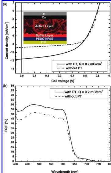
Figure 1a displays the illuminated current density-voltage (J-V) characteristics of the polymer solar cells fabricated with and without the PT layer inserted between the PEDOT: PSS layer and the active layer. The control device (ITO/ PEDOT:PSS/P3HT:PCBM/Ca/Al) exhibited an open circuit voltage (VOC) of 0.60 V, a short-circuit current density (JSC)
of 8.77 mA/cm2, and a fill factor (FF) of 66.5%, thereby
providing a PCE of 3.50%. After inserting the PT film through electrochemical deposition at an applied charge density of 0.2 mC/cm2, we observed an improvement in the value of JSC, thereby resulting in a PCE of 4.01%. Further improve-ment in PCE occurred after optimizing the thickness of the PT film. The best device performance (VOC) 0.59 V; JSC)
12.32 mA/cm2; FF ) 56.5 %; PCE ) 4.11%) was achieved
when the PT film was deposited at an applied charge density of 0.4 mC/cm2. The corresponding external quantum
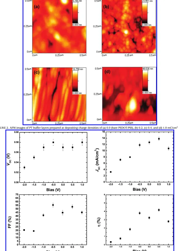
ef-ficiency (EQE) was shown in Figure 1b. Figure 2 presents atomic force microscopy (AFM) topographic images of the PEDOT:PSS film and the PT films grown at various charge densities. The topography of the PEDOT:PSS film was featureless, with a root-mean-square (RMS) roughness of 1.0 nm (Figure 2a). Electrochemical deposition of the PT film onto the PEDOT:PSS film resulted in significant changes in the surface morphology. When the deposition charge density was 0.2 mC/cm2, the surface of the PEDOT:PSS film was not
fully covered by the PT; instead, it was covered by PT islets. When the deposition charge density was 0.4 mC/cm2;
however, the surface was fully covered by the long grains of PT. The RMS surface roughness in this case was the lowest among those of all the samples featuring a PT layer, because the PT film filled up all the uncovered spaces on the surface. Higher charge densities (e.g., 1.0 mC/cm2) led to thicker
films, grainier morphologies, and larger RMS roughnesses. These AFM images confirmed that PT films could fully cover the PEDOT:PSS surface. Although the FF was lower when the devices featured an inserted PT film, the photogenerated current increased accordingly, presumably because the PT buffer layer blocked the n-type PCBM domain from directly contacting the PEDOT:PSS layer, thereby eliminating carrier recombination at the active layer-PEDOT:PSS interface. Moreover, the PT film behaved as an absorbed layer to generate a photocurrent. Therefore, elimination of carrier recombination at the active layer-PEDOT:PSS interface im-proved the photocurrent, consistent with our experimental data in panels a and b in Figure 1. Table 1 shows each character of devices with different deposition charge
densi-Table 1. Performances of Solar Cells Incorporating Buffer Layers of Various Thicknesses, Controlled by Varying the Charge Density during Electrodeposition Q (mC/cm2) V OC(V) JSC(mA/cm2) FF (%) η (%) Rs(Ω cm2) control 0.60 8.77 66.5 3.50 27.48 0.2 0.59 11.61 58.6 4.01 35.37 0.4 0.59 12.32 56.5 4.11 37.50 0.6 0.58 12.14 55.1 3.88 39.87 0.8 0.60 12.51 44.0 3.31 47.82 1.0 0.58 11.74 40.8 2.78 54.36
FIGURE 1. (a) J-V curves of solar cells prepared with and without a PT buffer layer. The depositing charge density (Q) was 0.2 mC/cm2. Inset: Device structure and relative position of the PT buffer layer. (b) EQEs of solar cells prepared with and without a PT buffer layer (Q ) 0.2 mC/cm2).
FIGURE 2. AFM images of PT buffer layers prepared at depositing charge densities of (a) 0.0 (bare PEDOT:PSS), (b) 0.2, (c) 0.4, and (d) 1.0 mC/cm2.
FIGURE 3. Variations in the values of (a) VOC, (b) JSC, (c) FF, and (d) PCE for solar cells incorporating buffer layers treated under various biases.
ties; we can see that the series resistances of the control device is 27.48 Ω cm2. When we introduce the buffer layer,
the overall thickness of the devices was increased leading to higher series resistance (Rs). The Rsvalue was increased
from 35.37 (0.2 mC/cm2) to 54.36 Ω cm2(1.0 mC/cm2). The
increasing resistance causes a decrease in FF (24). Because PT is an electrochromic material, the state of its films can be changed by applying a bias (25-28). To further optimize the device performance, we applied different biases (from -2.0 to +1.0 V, for 5 s) to the PT films in a solution of 0.1 M lithium perchlorate in acetonitrile prior to coating the active layers. Figure 3 presents the dependence of the device performance on the applied bias. We found that the cell performance varied considerably upon changing the treated bias. For example, the value of VOCwas quite low
when the PT film existed in its reduced state, but it increased upon increasing the treated bias from -0.2 to -0.5 V. Further increases in the treating bias did not affect the value of VOCappreciably, maintaining a value of ca. 0.57-0.58 V.
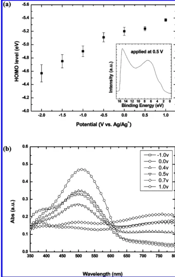
Figure 4 presents the HOMO energy levels of PT films treated under various applied biases; these values were obtained from UPS spectra. In the reduced state, the HOMO energy level of the PT film was lower than that in its natural state,
resulting in an increased energy barrier for carrier collection and, therefore, decreases in all of the device parameters. Upon increasing the treating bias, the HOMO energy level increased. In the oxidized state, the HOMO energy level of the PT film was ca. 5.1 eV, close to the reported values for P3HT (4.8-5.1 eV) (29, 30). Because oxidation can be regarded as the extraction of electrons from a material, the energy required to withdraw further electrons from PT increased, thereby increasing the HOMO energy level and improving the device parameters. The value of JSC of the
device increased upon increasing the treating bias from -0.2 to +0.5 V, but it decayed suddenly when increasing the treating bias further to +1.0 V (Figure 3b). The absorption spectrum in Figure 4b reveals that when the treating bias was +0.4 V, the PT film behaved as a semiconductor having an optical band gap of 1.85 eV (Eg) 1240/λ). Upon
increas-ing the applied bias, the PT film became more conductive. The absorption onset vanished when the treating bias increased to +0.7 V, suggesting that the PT film had become completely oxidized. Although the PT film possessed a higher HOMO energy level (Figure 4a) after it had been treated at a bias of greater than 0.7 V, it was no longer a semiconductor, but rather had become a conductor that could not prevent hole-electron recombination and could not absorb incident light to generate a photocurrent. The optimal cell performance occurred at a treating bias of +0.5 V, which provided a PT film existing in a transition state between a conductor and a semiconductor. This transition state en-sured that the characteristics of the buffer layer were between those of P3HT and PEDOT:PSS; thus, the buffer layer could finely connect each side and successfully block the PCBM layer from contacting the hole-transfer layer. This cell (prepared with a treating bias of +0.5 V) exhibited values of VOC, JSC, FF, and PCE of 0.57 V, 13.8 mA/cm2, 53%, and
4.18%, respectively.
In summary, we have improved the performance of a polymer solar cell by inserting a PT buffer layer between the active layer and the PEDOT:PSS layer. The PT buffer layer increased the photocurrent remarkablysand, therefore, the PCEsby reducing the degree of carrier recombination at the active layer-PEDOT:PSS junction. An innovative feature of this approach is that we can further tune the HOMO energy level by applying a bias to the buffer layer. The PCEs of these devices reached as high as 4.18% under illumination at 1 sun.
Acknowledgment. We thank the National Science Council
(NSC) of Taiwan (NSC 98-2221-E-001-002, NSC 96-2628-E-007-030-MY2) and Academia Sinica, Taiwan, for financial support.
REFERENCES AND NOTES
(1) Yu, G.; Gao, J.; Hummelen, J. C.; Wudl, F.; Heeger, A. J. Science
1995, 270, 1789 –1791.
(2) Krebs, F. C. Sol. Energy Mater. Sol. Cells 2009, 93, 394 –412. (3) Helgesen, M.; Sondergaard, R.; Krebs, F. C. J. Mater. Chem. 2010,
20, 36 –60.
(4) Kim, Y.; Coulis, S. A.; Nelson, J.; Bradley, D. D. C.; Cook, S.; Durrant, J. R. Appl. Phys. Lett. 2005, 86, 063502.
(5) Yu, B. Y.; Lin, W. C.; Huang, J. H.; Chu, C. W.; Lin, Y. C.; Kuo, C. H.; Lee, S. H.; Wong, K. T.; Ho, K. C.; Shyue, J. J. Anal. Chem.
2009, 81, 8936 –8941. FIGURE 4. (a) HOMO energy levels of PT films prepared under various
treating biases. (b) Relationship between the treating bias and the absorptions of the PT thin films.
(6) van Bavel, S.; Sourty, E.; de With, G.; Veenstrabd, S.; Loos, J. J. Mater. Chem. 2009, 19, 5388 –5393.
(7) Tromholt, T.; Gevorgyan, S. A.; Jørgensen, M.; Krebs, F. C.; Sylvester-Hvid, K. O. ACS Appl. Mater. Interfaces 2009, 1, 2768 – 2777.
(8) Tang, W.; Chellappan, V.; Liu, M.; Chen, Z. K.; Ke, L. ACS Appl. Mater. Interfaces 2009, 1, 1467–1473.
(9) Shi, J.; Peng, S.; Pei, J.; Liang, Y.; Cheng, F.; Chen, J. ACS Appl. Mater. Interfaces 2009, 1, 944 –950.
(10) Masuda, K.; Ikeda, Y.; Ogawa, M.; Benten, H.; Ohkita, H.; Ito, S. ACS Appl. Mater. Interfaces 2010, 2, 236 –245.
(11) Bertho, S.; Oosterbaan, W. D.; Vrindts, V.; D’Haen, J.; Cleij, T. J.; Lutsen, L.; Manca, J.; Vanderzande, D. Org. Electron. 2009, 10, 1248 –1251.
(12) Ayzner, A. L.; Tassone, C. J.; Tolbert, S. H.; Schwartz, B. J. J. Phys. Chem. C 2009, 113, 20050 –20060.
(13) Padinger, F.; Rittberger, R. S.; Sariciftci, N. S. Adv. Funct. Mater.
2003, 13, 85–88.
(14) Li, G.; Srotriya, V.; Huang, J.; Yao, Y.; Moriarty, T.; Emery, K.; Yang, Y. Nat. Mater. 2005, 4, 864 –868.
(15) Huang, J. H.; Yang, C. Y.; Ho, Z. Y.; Kekuda, D.; Wu, M. C.; Chu, C. W.; Ho, K. C. Org. Electron. 2009, 10, 27–33.
(16) Huang, J. H.; Chien, F. C.; Chen, P. L.; Ho, K. C.; Chu, C. W. Anal. Chem. 2010, 82, 1669 –1673.
(17) Krebs, F. C.; Gevorgyan, S. A.; Alstrup, J. J. Mater. Chem. 2009, 19, 5442–5451.
(18) Krebs, F. C. Org. Electron. 2009, 10, 761–768.
(19) Nishizawa, T.; Wei, Q.; Tajima, K.; Hashimoto, K. Adv. Mater.
2008, 20, 2211–2216.
(20) Liang, C. W.; Su, W. F.; Wang, L. Appl. Phys. Lett. 2009, 95, 133303.
(21) Bjerring, M.; Nielsen, J. S.; Nielsen, N. C.; Krebs, F. C. Macromol-ecules 2007, 40, 6012–6013.
(22) Gevorgyan, S. A.; Krebs, F. C. Chem. Mater. 2008, 20, 4386 –4390. (23) Huang, J. H.; Kekuda, D.; Chu, C. W.; Ho, K. C. J. Mater. Chem.
2009, 19, 3704 –3712.
(24) Kim, M. S.; Kim, B. G.; Kim, J. ACS Appl. Mater. Interfaces 2009, 1, 1264 –1269.
(25) Ruiz-Hitzky, E. Adv. Mater. 1993, 5, 334 –340. (26) Hyodo, K. Electrochim. Acta 1994, 39, 265–272.
(27) Galal, A.; Karago¨zler, A. E.; Shabana, R.; Amer, A.; Zimmer, H.; Mark, H. B., Jr. Sol. Energy Mater. Sol. Cells 1992, 25, 339 –348. (28) Kroon, R.; Lenes, M.; Hummelen, J. C.; Blom, P. W. M.; de Boer,
B. Polym. Rev. 2008, 48, 531–582.
(29) Huang, J. H.; Yang, C. Y.; Hsu, C. Y.; Chen, C. L.; Lin, L. Y.; Wang, R. R.; Ho, K. C.; Chu, C. W. ACS Appl. Mater. Interfaces 2009, 1, 2821–2828.
(30) Scharber, M. C.; Mu¨hlbacher, D.; Koppe, M.; Denk, P.; Waldauf, C.; Heeger, A. J.; Brabec, C. J. Adv. Mater. 2006, 18, 789 –794. AM100076A