國 立 交 通 大 學
電 子 工 程 學 系 電 子 研 究 所
碩 士 論 文
低功率指令快取記憶體之架構設計
Low-Power Instruction Cache
Architecture Design
研 究 生:程士祐
指導教授:黃俊達 博士
低功率指令快取記憶體之架構設計
Low-Power Instruction Cache Architecture Design
研 究 生:程士祐 Student: Shi-You Cheng
指導教授:黃 俊 達 博士 Advisor: Dr. Juinn-Dar Huang
國立交通大學
電子工程學系 電子研究所
碩士論文
A Thesis
Submitted to Department of Electronics Engineering & Institute of Electronics College of Electrical Engineering and Computer Science
National Chiao Tung University in Partial Fulfillment of the Requirements
for the Degree of Master in
Electronics Engineering July 2006
Hsinchu, Taiwan, Republic of China
低功率指令快取記憶體之架構設計
研究生:程士祐 指導教授:黃 俊 達 博士 國立交通大學 電子工程學系 電子研究所摘 要
近來,顯著的VLSI製程的進步已經不斷地提升處理器的速度以及DRAM的容量。 然而,這樣的進步也在處理器和主記憶體間產生了一個明顯且不斷增加的效能差 距。在處理器晶片上使用的快取記憶體為了就是替這主記憶體與處理器間的效能 差距搭起一座橋樑。為了更進一步改善記憶體系統的效能,最直觀的方法就是增 加快取記憶體的容量,以便增加快取記憶體命中的機率。然而這個方法也增加了 存取快取記憶體可觀的功率消耗。有鑒於此,低功率消耗的快取記憶體架構成為 了近來重要的課題之一。 在這個論文裡,我們提出一個低功率指令快取記架構,主要使用了四項技巧, 包括,記憶體次槽化、雙相位式快取記憶體、前置標籤確認以及為了略過存取標 籤記憶體所增加的循序訊號 "seq" 。藉由這些技巧,我們可以盡可能地排除不 必要的標籤記憶體以及資料記憶體的存取以達到低功率消耗的目標。實驗結果顯 示,相對於一個傳統的二路集合關聯式快取記憶體,我們提出的指令快取記憶體 可以減少大約54%的功率消耗。Low-Power Instruction Cache Architecture Design
Student: Shi-You Cheng Advisor: Dr. Juinn-Dar Huang
Department of Electronics Engineering & Institute of Electronics National Chiao Tung University
Abstract
Recent remarkable advances of VLSI technology have been increasing processor speed and DRAM capacity. However, the advances also have introduced a large, growing performance gap between processor and main memory. Cache memories have long been employed on processor chips in order to bridge the processor-memory performance gap. In order to improve the performance of the memory system further, the most straightforward approach is to increase the cache size, and then increase the cache-hit rates. However, this approach also increases the power dissipated in cache accesses significantly. Therefore, the low-power cache architectures have become one of the most important issues.
In this thesis, we propose a low-power instruction cache architecture by utilizing the four techniques, including memory sub-banking, two-phased cache, pre-tag checking, and signal “seq” for tag-memory access skipping. By these techniques, we can eliminate as many unnecessary tag-memory and data-memory accesses as possible to achieve the goal of low power consumption. Experimental results show that the proposed instruction cache can reduce about 54% power consumption compared to the conventional two-way set associative cache.
誌 謝
首先我要感謝我的指導教授 — 黃俊達博士,這兩年多來給我的支持與鼓勵, 讓我在研究上能自由發揮,每當遭遇到瓶頸以及困難時,老師也總會抽空與我詳 談,給予我適時的鼓勵及指導,感激之情,非隻字片語所可以形容。 也要感謝我的口試委員,清大資工—林永隆教授,交大電子—張添烜教授,在 百忙之中蒞臨指導,因為你們的寶貴意見讓我在研究上能更上一層樓。 也要感謝我一群實驗室的好伙伴,維聖、宏光、翊展、孝恩以及學弟們,因為 你們讓我在學習的道路上不孤單。相信我們更是一輩子的好朋友。 最後我很感謝我的父母親,由於他們辛勤的工作、無怨無悔的付出,讓我在研 究的這條道路上,能無後顧之憂,勇往直前。Contents
中文摘要 ...i
英文摘要 ... ii
誌謝 ... iii
Contents ...iv
Lists of Tables ...vi
Lists of Figures ... vii
Chapter 1 Introduction...1
1.1 Motivation ...1
1.2 Previous works for low-power consumption...2
1.3 Overview of the proposed low-power I-cache ...3
1.4 Thesis organization...3
Chapter 2 How A Conventional Cache Works...5
2.1 Block placement...5
2.2 Block identification...7
2.3 Block replacement...9
2.4 Write strategy ...10
2.5 An example of the cache architecture ...12
2.6 Power consumption of the cache...14
Chapter 3 Way-Predicting Set Associative Cache ...15
3.1 Concept ...15
3.2 Way prediction ...17
3.3 Organization...18
3.4 Conclusions ...20
Chapter 4 History-Based Tag-Comparison Instruction Cache...21
4.1 Concept ...21
4.3 Operation...24
4.4 Conclusions ...26
Chapter 5 Proposed Low-Power Instruction Cache ...27
5.1 Memory sub-banking ...27
5.2 Two-phased cache...30
5.3 Pre-tag checking ...33
5.4 Signal “seq” for tag-memory access skipping ...38
Chapter 6 Experimental Results ...41
6.1 Experiment setup...41
6.2 EDA environment ...42
6.3 Experimental results ...43
Chapter 7 Conclusions...45 Bibliography ...R-1
List of Tables
Table 2.1: Miss rates comparison for three replacement strategies ...10
Table 5.1: Power consumption of the memory sub-bank in an 8KB cache ...30
Table 5.2: Power consumption of the memory sub-bank in a 32KB cache ...30
Table 5.3: The ratio of WC I and WC II (part1) ...38
Table 5.4: The ratio of WC I and WC II (part2) ...38
Table 6.1: The cache types in the experiment ...42
Table 6.2: The technology and the EDA tools ...43
Table 6.3: Experimental result I ...43
Table 6.4: Experimental result II...44
List of Figures
Figure 2.1: This example cache has eight block frames and memory has 32 blocks...7
Figure 2.2: Block identification...8
Figure 2.3: Block identification of the example cache...13
Figure 2.4: The organization of the conventional cache ...13
Figure 3.1: Phased set associative cache ...16
Figure 3.2: Way-predicting set associative cache ...17
Figure 3.3: Organization of way-predicting four-way set associative cache ...19
Figure 4.1: Block diagram of a 4-way SA HBTC cache ...23
Figure 4.2: Operation-mode transition of HBTC cache ...25
Figure 5.1: The concept of memory sub-banking ...28
Figure 5.2: The address space partition for the memory sub-banking ...29
Figure 5.3: Example of memory sub-banking ...29
Figure 5.4: The cache hit in the two-phased two-way set associative cache ...32
Figure 5.5: The cache miss in the two-phased two-way set associative cache ...32
Figure 5.6: The address space partition for the pre-tag checking ...33
Figure 5.7: The architecture of a two-phased cache with pre-tag checking...34
Figure 5.8: Better case I of the two-phased case with pre-tag checking ...36
Figure 5.9: Better case II of the two-phased case with pre-tag checking...36
Figure 5.10: Worse case I of the two-phased case with pre-tag checking ...37
Figure 5.11: Worse case II of the two-phased case with pre-tag checking ...37
Figure 5.12: Sequential access graph and example ...40
Chapter 1
Introduction
1.1 Motivation
VLSI technologies have been increasing processor speed and DRAM capacity
dramatically. However, they also have introduced a large, growing performance gap
between processors and main memory (DRAM). By improving not only the clock speed
but also instruction level parallelism (ILP), the processor performance has been
improving at a rate of 60% per year. On the other hand, the access time to DRAM has
been improving at a rate of less than 10% per year [1]. Moreover, current memory
systems suffer from a lack of memory bandwidth caused by I/O pin bottleneck. This
problem is known as “Memory Wall” [2], [3]. The inability of memory systems causes
poor overall system performance in spite of higher processor performance.
Cache memory has been playing an important role in bridging the performance gap
between high-speed processor and low-speed off-chip main memory because confining
memory accesses on-chip reduces memory access latency. In order to improve the
performance of the memory system further, the most straightforward approach is to
increase the cache size. Increasing the cache capacity reduces the frequency of off-chip
accesses due to the improvement of cache-hit rates. However, this approach also
of caches, several studies are reported. The power consumption of on-chip caches for
StrongARM SA110 occupies 43% of the total chip power [4]. In the 300 MHz bipolar
CPU reported by Jouppi et al [5], 50% of power is dissipated by caches. Recent growing
mobile-market strongly requires not only high performance but also low-power
dissipation. One of uncompromising requirements of portable computing is power
efficiency because that directly affects the battery life. Therefore, from these studies, we
believe that considering low-power cache architectures is a worthwhile work for the
future processor systems.
1.2
Previous works for low-power consumption
In conventional set associative caches, all ways are searched in parallel because the
cache access time is critical. In fact, on a cache hit, only one way has the data desired by
the processor. Therefore, the access to the remaining ways is unnecessary. The previous
works as follows attempt to avoid the unnecessary way activation, or the unnecessary tag
look-ups to reduce the power consumption:
z Way-predicting cache [6]: The way-predicting set associative cache predicts which way has the data desired by the processor before starting the cache access.
The way prediction is performed based on memory-access history recorded by
the way-prediction table. If prediction is correct, cache consumes power for only
one activated way. Otherwise, the cache searches all of the ways and consumes
power for all of them. In addition to this power consumption, miss prediction
also causes additional cycles which make performance degrade. (We will
introduce the detail of the way-predicting cache in Chapter 3.)
cache and attempts to eliminate unnecessary tag comparison. In conventional
caches, tag comparison has to be performed on every cache access in order to
test whether the memory reference hits the cache. Execution footprints recorded
in a BTB (branch target buffer) is used for the prediction. However, not all the
processors use the BTB technique. It has a limitation on hardware
implementation. (We will introduce the detail of the history-based
tag-comparison cache in Chapter 4.)
1.3
Overview of the proposed low-power I-cache
We propose a new low-power instruction cache architecture which has the advantage
of simple hardware implementation by using the four techniques as follows: z Memory sub-banking
z Two-phased cache z Pre-tag checking
z Signal “seq” for tag-memory access skipping
By these techniques, we can eliminate as many unnecessary tag-memory and
data-memory accesses as possible to achieve the goal of low power consumption.
The experimental results show that the proposed 8KB instruction cache in 16-byte
blocks with two-way set associative placement reduces about 54% power consumption
1.4 Thesis
organization
This thesis introduces the low-power instruction cache architecture design, and is
organized as follows. Chapter 2 explains how a conventional cache works. Chapter 3
introduces the details of the way-predicting set associative cache, and Chapter 4
introduces the detail of the history-based tag-comparison cache. In Chapter 5, we present
our own low-power instruction cache architecture. Chapter 6 shows the experimental
Chapter 2
How A Conventional Cache Works
In this chapter, we will describe how a conventional cache [9] works by answering the
four common questions about the cache:
Q1: Where can a block be placed in the cache? (block placement)
Q2: How is a block found if it is in the cache? (block identification)
Q3: Which block should be replaced on a miss? (block replacement)
Q4: What happens on a write? (write strategy)
Besides, we will take an example of the cache architecture and discuss the power
consumption of the cache we care about most.
2.1 Block
placement
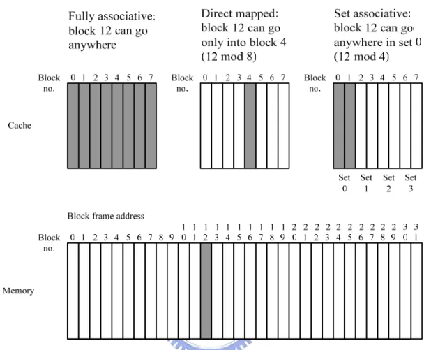
Figure 2.1 shows that the restrictions on where a block is placed create three
categories of cache organization:
z If each block has only one place it can appear in the cache, the cache is said to be direct mapped. The mapping is usually
z If a block can be placed anywhere in the cache, the cache is said to be fully associative.
z If a block can be placed in a restricted set of places in the cache, the cache is set associative. A set is a group of blocks in the cache. A block is first mapped onto a
set, and then the block can be placed anywhere within that set. The set is usually
chosen by bit selection; that is,
(Block address) MOD (Number of sets in cache)
If there are n blocks in a set, the cache placement is called n-way set associative.
Take Figure 2.1 for example. The three options for caches are shown left to right. In
fully associative, block 12 from the lower level can go into any of the eight block frames
of the cache. With direct mapped, block 12 can only be placed into block frame 4 (12
modulo 8). Set associative, which has some of both features, allows the block to be placed
anywhere in set 0 (12 modulo 4). With two blocks per set, this means block 12 can be
placed either in block 0 or in block 1 of the cache. Real caches contain thousands of block
frames and real memories contain millions of blocks. The set-associative organization
has four sets with two blocks per set, called two-way set associative. Assume that there is
nothing in the cache and that the block address in question identifies lower-level block
12.
The range of caches from direct mapped to fully associative is really a continuum of
levels of set associativity. Direct mapped is simply one-way set associative, and a fully
associative cache with m blocks could be called “m-way set associative.” Equivalently,
direct mapped can be thought of as having m sets, and fully associative as having one set.
The vast majority of processor caches today are direct mapped, two-way set
Figure 2.1: This example cache has eight block frames and memory has 32 blocks
2.2 Block
identification
Caches have an address tag on each block frame that gives the block address. The tag
of every cache block that might contain the desired information is checked to see if it
matches the block address from the CPU. As a result, all possible tags are searched in
parallel because speed is critical.
There must be a way to know that a cache block does not have valid information. The
most common procedure is to add a valid bit to the tag to say whether this entry contains
Figure 2.2: Block identification
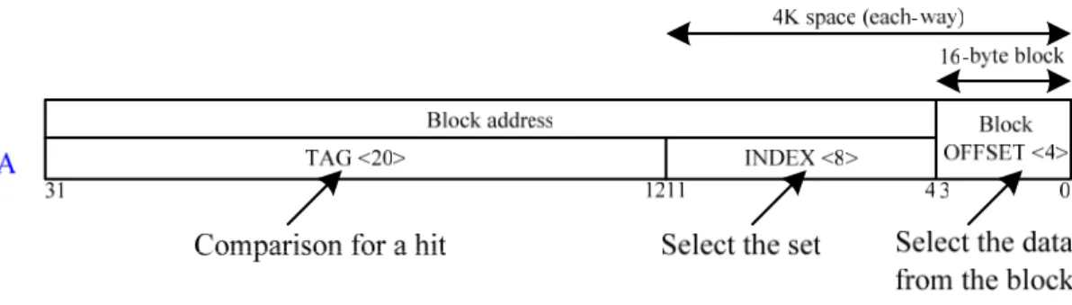
Before proceeding to the next question, let’s explore the relationship of a CPU
address to the cache. Figure 2.2 shows how an address is divided. The first division is
between the block address and the block offset. The block frame address can be further
divided into the tag field and the index field. The block offset field selects the desired data
from the block, the index field selects the set, and the tag field is compared against PC for
a hit. Although the comparison could be made on more bits of the address than the tag bits,
there is no need because:
z The offset should not be used in the comparison, since the entire block is present or not, and hence all block offsets result in a match by definition.
z Checking the index is redundant, since it was used to select the set to be checked. An address stored in set 0, for example, must have 0 in the index field or it
couldn’t be stored in set 0; set 1 must have an index value of 1; and so on. This
optimization saves hardware and power by reducing the width of memory size
for the cache tag.
If the total cache size is kept the same, increasing associativity increases the number
of blocks per set, thereby decreasing the size of the index and increasing the size of the
tag. That is, the tag-index boundary in Figure 2.2 moves to the right with increasing
2.3 Block
replacement
When a miss occurs, the cache controller must select a block to be replaced with the
desired data. A benefit of direct-mapped placement is that hardware decisions are
simplified - in fact, so simple that there is no choice: Only one block frame is checked
for a hit, and only that block can be replaced. With fully associative or set-associative
placement, there are many blocks to choose from on a miss. There are three primary
strategies employed for selecting which block to be replaced:
z Random - To spread allocation uniformly, candidate blocks are randomly selected. Some systems generate pseudorandom block numbers to get
reproducible behavior, which is particularly useful when debugging hardware. z Least-recently used (LRU)-To reduce the chance of throwing out information
that will be needed soon, accesses to blocks are recorded. Relying on the past to
predict the future, the block replaced is the one that has been unused for the
longest time. LRU relies on a corollary of locality: If recently used blocks are
likely to be used again, then a good candidate for disposal is the least-recently
used block.
z First in, first out (FIFO)-Because LRU can be complicated to calculate, this approximates LRU by determining the oldest block rater than the LRU.
A virtue of random replacement is that it is simple to build in hardware. As the
number of blocks to keep track of increase, LRU becomes increasingly expensive and is
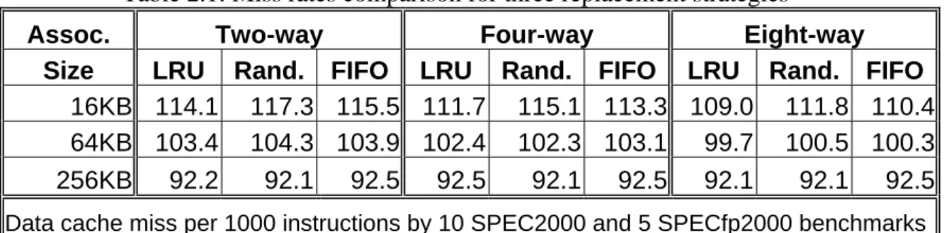
frequently only approximated. Table 2.1 shows the difference in miss rates between LRU,
Table 2.1: Miss rates comparison for three replacement strategies
Assoc. Two-way Four-way Eight-way
Size LRU Rand. FIFO LRU Rand. FIFO LRU Rand. FIFO
16KB 114.1 117.3 115.5 111.7 115.1 113.3 109.0 111.8 110.4 64KB 103.4 104.3 103.9 102.4 102.3 103.1 99.7 100.5 100.3 256KB 92.2 92.1 92.5 92.5 92.1 92.5 92.1 92.1 92.5
Data cache miss per 1000 instructions by 10 SPEC2000 and 5 SPECfp2000 benchmarks
2.4 Write
strategy
Modifying a block cannot begin until the tag is checked to see if the address is a hit.
Because tag checking cannot occur in parallel, writes normally take longer than reads.
The write policies often distinguish cache designs. There are two basic options when
writing to the cache:
z Write through- The information is written to both the block in the cache and to the block in the lower-level memory.
z Write back- The information is written only to the block in the cache. The modified cache block is written to main memory only when it is replaced.
To reduce the frequency of writing back blocks on replacement, a feature called the
dirty bit is commonly used. This status bit indicates whether the block is dirty (modified
while in the cache) or clean (not modified). If it is clean, the block is not written back on
a miss, since identical information to the cache is found in lower levels.
Both write back and write through have their advantages. With write back, writes
occur at the speed of the cache memory, and multiple writes within a block require only
one write to the lower-level memory. Since some writes don’t go to memory, write back
buses less than write through, it also saves power, making it attractive for embedded
applications.
Write through is easier to implement than write back. The cache is always clean, so
unlike write back read miss never result in writes to the lower level. Write through also
has the advantage that the next lower level has the most current copy of the data, which
simplifies data coherency. Data coherency is important for multiprocessors and for I/O.
As we see, I/O and multiprocessors are fickle: They want write back for processor
caches to reduce the memory traffic and write through to keep the cache consistent with
lower levels of the memory hierarchy.
When the CPU must wait for writes to complete during write through, the CPU is said
to have a write stall. A common optimization to reduce write stalls is a write buffer,
which allows the processor to continue as soon as the data are written to the buffer,
thereby overlapping processor execution with memory updating. As we will see shortly,
write stalls can occur even with write buffer.
Since the data is not needed on a write, there are two options on a write miss:
z Write allocate- The block is allocated on a write miss, followed by the write hit actions above. In this natural option, write miss acts like read miss.
z No-write allocate- This apparently unusual alternative is write misses do not affect the cache. Instead, the block is modified only in the lower-level memory.
Thus, blocks stay out of the cache in no-write allocate until the program tries to read
the blocks, but even blocks that are only written will still be in the cache with write
allocate. Normally, write-back caches use write allocate, hoping that subsequent writes to
that block will be captured by the cache. Write-through caches often use no-write allocate.
The reasoning is that even if there are subsequent writes to that block, the writes must still
2.5
An example of the cache architecture
Take an 8KB cache in 16-byte blocks with two-way set associative placement for
example. Figure 2.3 shows the block identification of the example cache. The physical
address coming into the cache is divided into tow fields: the 28-bit block address and the
4-bit block offset (16 = 24 and 28 + 4 = 32). The block address is further divided into an
address tag and cache index. Step 1 shows this division.
The cache index selects the tag to be tested to see if the desired block is in the cache.
The size of the index depends on cache size, block size, and set associativity. For our
example, the set associativity is set to two, and we calculate the index as follows:
8 4 13 Index
2
2
2
2
ity
associativ
Set
size
Block
size
Cache
2
=
×
=
×
=
(2.1)Hence, the index is 8 bits wide, and the tag is 28-8 = 20 bits wide. Although that is the
index needed to select the proper block, 16 bytes is much more than the CPU wants to
consume at once. Hence, it makes more sense to organize the data portion of the cache
memory 4 bytes wide, which is the natural data word of the processor. Thus, in addition to
8 bits to index the proper cache block, 2 more bits from the block offset are used to index
Figure 2.3: Block identification of the example cache
Index selection is step 2 in Figure 2.4. The two tags and the two data are read from the
cache. After reading two tags from the cache, they are compared to the tag portion of the
block address from the CPU. This comparison is step 3 in the Figure 2.4 (To be sure the
valid bit must be set or else the results of the comparison are ignored). The final step is to
use the comparison result to select the proper data from the data cache memory.
2.6
Power consumption of the cache
The cache-access power depends on the power dissipated for the SRAM access [6]
[10]. We simplify the cache-access power as follows:
SRAM Cache
P
P
≈
(2.2) Data Data Tag TagP
N
P
N
×
+
×
=
(2.3) z NTag, NData: The average number of tag-memory and data-memory to beactivated for a cache access.
z PTag, PData: Power dissipated for a tag-memory access and that for a
data-memory access, respectively.
In conventional set-associative caches, all the ways are activated regardless of hits or
misses, and the cache access can be completed in one cycle. Accordingly, average
cache-access power (PCache) and time (TCache) of a conventional two-way set associative
(2SACache) can be expressed by the following equations:
Data Tag SACache
P
P
P
2=
2
+
2
(2.4)Cycle
T
2SACache=
1
(2.5) It needs two tag-memory and two data-memory accesses during each cache access, so the(NTag, NData) = (2, 2).
However, In fact, on a cache hit, only one way has the data desired by the processor.
In other words, accesses of the other way are unnecessary. In order to reduce the power
consumption of the cache, we must try to reduce NTag & NData as possible during each
cache access.
Besides, we find that the entire memory block is enabled just in order to access one
word (one tag for comparison or one data). We can partition a large memory block into
several small blocks. During each memory access, we just enable one of these small
Chapter 3
Way-Predicting Set Associative Cache
In this chapter, we introduce a low power cache architecture using the way prediction,
called way-predicting set-associative cache [6]. The way-predicting set-associative cache
speculatively selects one way, which is likely to contain the data desired by the processor,
from the set designated by the memory address, before it starts the normal cache access.
The correct way-prediction makes it possible to eliminate the unnecessary way activation,
so that the energy can be saved. However, the miss prediction makes the cache searches
all of the ways and consumes power all of them. Besides, it also causes additional cycles
which make performance degradation.
3.1 Concept
The way-prediction set associative cache speculatively chooses one way before
starting the normal cache-access process. Then the cache divides the cache-access
process into two phases, like the phased set associative cache [11] as shown in Figure 3.1,
Figure 3.1: Phased set associative cache
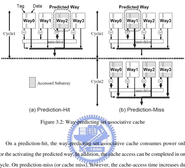
z Cycle 1: Both of a tag and a block frame from only the predicted-way are read out, and then the tag comparison is performed. If the tag-comparison result is a
match, the data desired by the processor is provided from the block frame read
out, and the cache access is completed successfully. In this case, the
way-predicting set-associative cache behaves as a direct-mapped cache, as
shown in Figure 3.2(a). If the tag-comparison result is not a match, then the
second phase is performed.
z Cycle 2: The cache searches the other remaining ways in parallel, as shown in Figure 3.2(b). If one of the tag-comparison results is a match, the data from the
hit way is provided to the processor. Otherwise, a cache replacement takes place.
Namely, the way-predicting set associative cache behaves as a “three-way” set
Figure 3.2: Way-predicting set associative cache
On a prediction-hit, the way-predicting set associative cache consumes power only
for the activating the predicted way. In addition, the cache access can be completed in one
cycle. On prediction-miss (or cache miss), however, the cache-access time increases due
to the successive process of two phases as shown in Figure 3.2(b). Since all the remaining
ways are activated in the same manner as conventional set associative caches, the
way-predicting set associative cache cannot reduce power consumption in this scenario.
The performance / power efficiency of the way-predicting set associative cache
largely depends on the accuracy of the way prediction.
3.2 Way
prediction
Many application programs have higher locality of memory references. This means
that a block frame referenced by the processor will be referenced to again in the near
Here, it is assumed that a seti is accessed by a processor for cache look-up, and a wayj
(0 ≦ j ≦ AS - 1, where AS is cache associativity) causes a cache hit. In this case, the
data required by the processor will reside in the wayj on a near future access to the seti if
program have higher locality of memory references. Accordingly, the way-predicting set
associative cache employs a way-prediction policy based on MRU (Most Recently Used)
algorithm. The way predictor determines a predicted way for the set which has being
accessed by the process as follows:
z On prediction-hits, the way predictor does nothing because the current way-prediction is correct.
z On prediction-misses (but cache hit), the way predictor regards the way having the data desired by the processor as the predicted way. The predicted way can be
determined by tag comparison results.
z On cache-misses, the way predictor regards the way to be filled on cache replacement as the predicted way. The predicted way can be determined by the
results of tag comparisons (hit or miss) and status flags indicating which way to
be replaced.
3.3 Organization
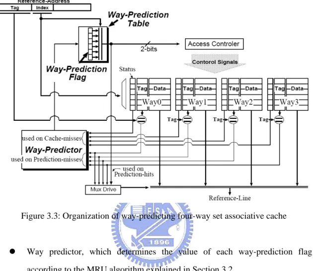
Figure 3.3 gives an organization of the way-predicting four-way set associative cache.
Compared to the conventional four-way set associative, it needs the following additional
components:
z Way-prediction table, which contains a two-bit flag (way-prediction flag) for each set. The two-bit flag is used to speculatively choose one way from the
Figure 3.3: Organization of way-predicting four-way set associative cache
z Way predictor, which determines the value of each way-prediction flag according to the MRU algorithm explained in Section 3.2.
The way-predicting four-way set associative cache works as follows:
1. The way-prediction flag associated with a given set is accessed, and is read from the
way-prediction table immediately after an effective memory address is generated.
The predicted way is determined by the way-prediction flag read out.
2. Only the predicted way is activated, and the tag and the block frame associated with
the predicted way are read simultaneously. The tag is then compared with the
tag-portion of the memory address. If the tag-comparison result is a match (prediction
hit), the cache access completes successfully. Otherwise (prediction miss), Steps 3
3. The remaining three ways are activated, and all the tags and the block frames are read
out in parallel. Then, the three tags are compared with the tag-portion of the memory
address. If at most on tag matches, the way-predicting set associative cache provides
the referenced data to the processor. Otherwise (cache miss), a cache replacement
takes place.
4. The way predictor modifies the way-prediction flag based on the result of
replacement strategies. The modified way-prediction flag is written back to the
way-prediction table.
3.4 Conclusions
The performance / power efficiency of the way-predicting set associative cache
largely depends on the accuracy of the way prediction. The miss prediction makes the
cache search all of the ways and consume all power of them. In other words, the
way-predicting set associative cache cannot reduce power consumption in this scenario.
The miss prediction also causes additional cycles which cause performance degradation.
Besides, the way-prediction table is also a significant area overhead compared to the
Chapter 4
History-Based Tag-Comparison Instruction
Cache
In this chapter, we introduce a low-power instruction cache architecture, called
history-based tag-comparison (HBTC) cache [7] [8]. The HBTC cache attempts to reuse
tag-comparison results to eliminate the power consumption of tag comparison, including
the tag-memory accesses further. The cache records tag-comparison results in an
extended branch target buffer (BTB), and reuses them for directly selecting only the
hit-way which includes the target instruction. In this scenario, the (NTag, NData) is equal to
(0, 1) in Equation (2.3). However, not all the processors employ BTB technique.
Naturally, the HBTC cache has a limitation in the hardware. In other words, the HBTC
cache can be only used in processors which have employed the BTB technique.
4.1 Concept
The content of cache memory is updated when cache misses take place. Instruction
caches can achieve much higher cache hit rates due to rich locality of memory references.
There are many loops in programs, so that some instruction blocks will be executed in
many times. We call a run-time instruction block “a dynamic basic-block”. The dynamic
basic-block consists of one or more successive basic blocks. The top of the dynamic
basic-block is addressed by a branch-target address, and the end of it is addressed by a
taken-branch or jump address. Therefore, not-taken conditional branches might be
included in the dynamic basic-block.
The dynamic basic-block is executed many times during program execution. On the
first time of the dynamic basic-block execution, the tag comparison for all instructions
has to be performed. However, on the second execution, if no cache miss has occurred
since the first execution, it is guaranteed that the dynamic basic-block resides in the cache.
Hence, we can determine that the indexed cache entry corresponds to the requested
address without performing the tag comparison.
When a dynamic basic-block is executed, the history-based tag-comparison cache
attempts to avoid unnecessary tag comparisons by detecting the following conditions:
1. The dynamic basic-block has been executed, and
2. No cache miss has occurred since the previous execution of the dynamic
basic-block.
The history-based tag-comparison cache omits the tag comparison when the above
conditions are satisfied regardless of the intra-line and inter-line flows.
4.2 Organization
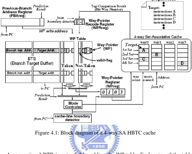
As shown in Figure 4.1, the HBTC cache requires six additional components:
Way-Pointer table (WP table), Way-Pointer Register (WPreg), Way-Pointer Record
Figure 4.1: Block diagram of a 4-way SA HBTC cache
A conventional BTB is extended by adding the WP table. Each entry of the table
corresponds to that of the BTB, and consists of two of M way-pointers. A tag-comparison
result (i.e., hit-way number) is stored in the extended BTB as a way pointer (WP).
Therefore, the WP can be implemented as a log n-bit flag where n is the cache
associativity, and specifies the hit-way of the corresponding instructions. The 1-bit valid
flag is used for determining whether the M of WPs are valid or not. The taken WPs are
used for the target instructions, and the not-taken WPs are used for the fall-through
instructions of the corresponding branch in the BTB. In Figure 4.1, for example, cache
line A, B, C, and D are referenced sequentially after a taken branch is executed. In this
case, the tag-comparison results (or the hit-way numbers) for their references are 0, 1, 0,
and 3. This information is stored in the WP table, and is reused when the target
At the first reference of instruction of instructions, we have to perform tag checks. In
order to record the generated tag-comparison results in the WP table, the WPRreg is used
as a temporal register. The PBAreg stores the previous-branch-instruction address and
the result of branch prediction (taken or not-taken), and is used as an address register to
store the value of WPRreg to the WP table. At every BTB hit, the WPs read from the BTB
is stored in the WPreg, and are provided to the I-cache for tag-comparison re-use. The
mode controller manages the HBTC behavior. The details of the HBTC operation are
explained in Section 4.3.
In order to reuse the tag-comparison results at cache-line granularity, we need to
detect cache-line boundary for instruction references. This can be done by monitoring a
few bits of the PC [12]. (It uses BTB hit to hint that the successive instructions are
sequential flow.)
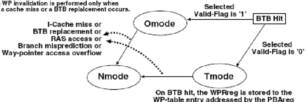
4.3 Operation
The HBTC cache has the following three operation modes, one of which is activated
by the mode controller:
z Normal mode (Nmode): The cache behaves as a conventional I-cache, so that the tag check is performed at every cache access (the (NTag, NData) is equal to (n, n) in
Equation (2.3)).
z Omitting mode (Omode): The cache reuses tag comparison results, so that only the hit way is activated with performing tag checks (the (NTag, NData) is equal to
(0, 1) in Equation (2.3)).
z Tracing mode (Tmode): The cache works as the same as the Nmode the (NTag,
Figure 4.2: Operation-mode transition of HBTC cache
tag-comparison results generated by the I-cache (this operation is not performed
in the Nmode).
Figure 4.2 shows the operation transitions. On every BTB hit, the HBTC cache reads
in parallel both the taken and not-taken WPs associated with the BTB-hit entry, and
selects one of them based on the branch prediction result. If the selected valid flag is ‘1’,
the operation enters the Omode and the selected WPs are stored to the WPreg. Otherwise
the Tmode is activated, and both the branch instruction address (PC) and the branch
prediction result (taken or not-taken) are stored to the PBAreg.
In the Omode, whenever a cache-line boundary is detected, the next WP in the WPreg
is selected. On the other hand, in the Tmode, the tag-comparison results generated by the
I-cache are stored to the WPRreg at cache-line granularity. When the next BTB hit occurs
in the Tmode, the value of the WPRreg is written into the WP-table entry pointed by the
PBAreg and the corresponding valid-flag is set to ‘1’.
The WPreg and the WPRreg can hold WPs up to M, where M is the total number of
if the cache attempts to access the M + 1-th WP in the WPreg or WPRreg, WP-access
overflow occurs and the operation switches to the Nmode.
Whenever a cache miss takes place, all WPs recorded in the WP table are invalided by
resetting all the valid-flags to ‘0’ and operation transits to the Nmode. This is because
instructions corresponding to valid WPs may be evicted from the cache.
In the Tmode, when a BTB hit occurs just after L (L < M) of tag-comparison results
are written in the WPRreg. Some of invalid WPs are stored to the WP table. We assume
that no BTB replacement has occurred since the previous Tmode. Under this assumption,
it is guaranteed that the BTB-entry makes the next BTB hit just after L of valid WPs are
accessed. Since the WPreg is overwritten by the next BTB hit , there is no chance to be
used for the M - L of invalid WPs. In order to guarantee this assumption, the cache
performs WP invalidation and changes the operation mode to the Nmode whenever not
only a cache moss takes place but also a BTB replacement occurs.
The cache operates in the Nmode whenever a branch-target address is provided by a
return address stack (RAS), or a branch mis-prediction is detected (WP invalidation is not
performed).
4.4 Conclusions
The cache records tag-comparison results in an extended branch target buffer (BTB).
However, not all the processors employ BTB technique. Naturally, the HBTC cache has a
limitation on the hardware implementation. In other words, the HBTC cache can be only
used in processors which have employed the BTB technique.
Size of the WP table in proportion to the number M of WPs is a significant area
Chapter 5
Proposed Low-Power Instruction Cache
In this chapter, we propose our low-power instruction cache architecture with four
techniques as follows to reduce the power consumption of cache memory.
1. Memory sub-banking [13].
2. Two-phase cache.
3. Pre-tag checking.
4. Signal “seq” for tag-memory access skipping.
5.1 Memory
sub-banking
In conventional SA caches, we find that the entire memory block is enabled just in
order to access one word (one data or one tag for comparison). We can partition a large
memory block into several small blocks. During each memory access, we just enable one
of these small blocks where the critical word is at and just consume the power of the small
block.
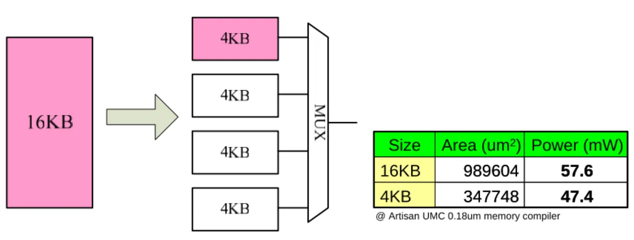
Figure 5.1 shows the concept of memory sub-banking. We partition a 16KB memory
47.4 347748 4KB 57.6 989604 16KB Power (mW) Area (um2) Size 47.4 347748 4KB 57.6 989604 16KB Power (mW) Area (um2) Size
@ Artisan UMC 0.18um memory compiler
Figure 5.1: The concept of memory sub-banking
only the desired sub-bank. The 4-to-1 multiplexer is also needed to choose the correct
output data. In the example, we can reduce about (57.6-47.4) / 57.6 = 17.7% power
consumption of a 16KB memory bank. However, we also have a (347748 × 4-989604) /
989604 = 40.5% area overhead of a 16KB memory bank. Therefore, memory
sub-banking is a trade-off between power and area.
Figure 5.2 shows the address space partition for the memory sub-banking in a cache.
The sum of the SUB field width and Sub-Index field width is equal to the original INDEX
field width. The SUB field width depends on the number of memory sub-banks. For
example, we decide to partition the tag-memory into four sub-banks and the data-memory
into eight sub-banks. The SUB field width is 2-bit and 3-bit individually. The Sub-Index
field is the set selection of the sub-bank.
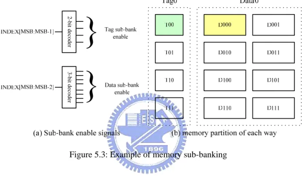
Figure 5.3 (a) shows a 2-bit sub-bank address decoder is needed to generate control
signals for the four tag-memory sub-banks. A 3-bit sub-bank address decoder is needed to
generate control signals for the eight data-memory sub-banks.
Figure 5.3 (b) shows the memory partition of each way in a cache. Only 1/4
Figure 5.2: The address space partition for the memory sub-banking 2 -bit decoder 3-b it deco der
Figure 5.3: Example of memory sub-banking
In order to discuss the power efficiency further due to the memory sub-banking
technique, we use Artisan UMC 0.18um memory compiler to do the power analysis for
the memory sub-bank. Table 5.1 shows the power consumption of the memory sub-bank
in an 8KB cache. “No sub” means that the memory is not partitioned. “SubN” means that
the memory is partitioned into N sub-banks. We can see that the power consumption of
the tag-memory is almost not improved whether we perform memory sub-banking or not.
The power consumption of the data-memory is just reduced by 2.5 mW (47.4-44.9 = 2.5)
about 5% improvement. Table 5.2 shows the power consumption of the memory
sub-bank in a 32KB cache. The power consumption of the data-memory is reduced by
Table 5.1: Power consumption of the memory sub-bank in an 8KB cache
8KB cache size(2-Way set associative, 16Byte Line)
Tag Memory Data Memory
Type Size Power (mW) Type Size Power (mW)
No sub 256x20 28.5 No sub 1024x32 47.4
Sub2 128x20 28.2 Sub2 512x32 46.0
Sub4 64x20 28.0 Sub4 256x32 45.3
Sub8 128x32 44.9
Table 5.2: Power consumption of the memory sub-bank in a 32KB cache
32KB cache size (2-Way set associative, 16Byte Line)
Tag Memory Data Memory
Type Size Power(mW) Type Size Power (mW)
No sub 1024x18 27.8 No sub 4096x32 57.6
Sub2 512x18 26.4 Sub2 2048x32 50.2
Sub4 256x18 25.7 Sub4 1024x32 47.4
Sub8 512x32 46.0
Based on these experimental results, we find that the memory sub-banking technique
should be used for a larger cache size, say, more than 32KB.
5.2 Two-phased
cache
Although at most only one way has the data desired by the processor, all the ways are
accessed in parallel in conventional set associative caches. Thus, a lot of power is wasted.
To solve this issue, Hasegawa et al proposed a low-power set associative cache
architecture [11] called phased set associative cache. The phased set associative cache is
and 2 PData, power reduction from the conventional two-way set associative cache on
cache hits, and cache misses, respectively. The average power consumption in a phased
two-way set associative cache (PP2SACache) for a cache access can be expressed as follows:
Data Tag
SACache
P
P
CHR
P
P
2= 2
+
×
(5.1)Here, CHR is the cache hit rate. However, all the cache accesses are delayed one cycle.
This latency significantly slows down the overall performance.
In order to solve the latency, we propose a new architecture which is similar to phased
set associative cache called two-phased set associative cache. We use posedge-trigger
tag-memory and negedge-trigger data-memory to make one-cycle cache accesses
possible.
Figure 5.4 shows the cache hit in the two-phased two-way set associative cache (8KB
cache size, 16-byte block). The cache accesses the tag-memory and do tag comparison in
all the ways during the high half-cycle and sequentially accesses the data-memory for the
desired data in the matching way during the low half-cycle.
Figure 5.5 shows the cache miss in the two-phased two-way set associative cache
(8KB cache size, 16-byte block). Due to no matching way during the high half-cycle, no
data-memory will be activated in the low half-cycle. The average power consumption in a
two-phased two-way set associative cache (P2P2SACache) for a cache access is the same
with the Equation (5.1).
However, the timing of the two-phased cache becomes more critical than the phased
cache. Because the tag-memory access and the tag comparison must be done within
5.3 Pre-tag
checking
Due to the locality principle of program, the addresses of instructions loaded to the
cache are not far away between each other. This means that the least significant bits of the
tag field are usually different, but the most significant bits of the tag field are usually the
same. In other words, the tag comparison with the few least significant bits can almost
decide if the cache hits or not. In order to reduce the power consumption of the
tag-memory further, we propose a technique called pre-tag checking used with the
two-phased set associative cache. We take 3 least significant bits (TAG[LSB+2: LSB]) to
do pre-tag checking for way selection.
Figure 5.6 shows the address space partition in a 2-way set associative cache (8KB,
16-byte block) for the pre-tag checking.
Figure 5.6: The address space partition for the pre-tag checking
Figure 5.7 shows the architecture of the two-phased cache with pre-tag checking.
During the high half-cycle, the cache accesses the ptag-memory and does pre-tag
comparison with the 3-bit PTAG field in the address for the way selection. During the low
half-cycle, the cache accesses the otag-memory and data-memory in parallel in the
matching way selected by the PTAG comparison result. The OTAG comparison result is
Figure 5.7: The architecture of a two-phased cache with pre-tag checking
The cache-access power can be expressed as follows:
Data Data OTag OTag PTag PTag Cache
N
P
N
P
N
P
P
=
×
+
×
+
×
(5.2)There are four cases for the power consumption in the two-phased two-way set
associative cache with pre-tag checking. Among them, there are two better cases and two
worse cases for the power consumption compared to the two-phased two-way set
associative cache without pre-tag checking.
z BC I: Figure 5.8 shows the better case I for the power consumption. The PTAG comparison result indicates that there is one way matching. The otag-memory
and data-memory in the matching way are activated, and the OTAG comparison
result indicates that the cache actually hits. In this case, the (NPTag, NOTag, NData)
z BC II: Figure 5.9 shows the better case II for the power consumption. The
PTAG comparison result indicates that there is no way matching (cache miss).
Therefore, no otag-memory and data-memory will be activated. In this case, the
(NPTag, NOTag, NData) is equal to (2, 0, 0).
z WC I: Figure 5.10 shows the worse case I for the power consumption. The
PTAG comparison result indicates that there are two ways matching. The
otag-memory and data-memory in the matching ways are activated, and the
OTAG comparison result indicates that the cache actually hits or misses. In this
case, the (NPTag, NOTag, NData) is equal to (2, 2, 2).
z WC II: Figure 5.11 shows the worse case II for the power consumption. The
PTAG comparison result indicates that there is one way matching. The
otag-memory and data-memory in the matching way are activated, but the
OTAG comparison result indicates that the cache actually misses. In this case,
the (NPTag, NOTag, NData) is equal to (2, 1, 1).
On the basis of our previous discussion, according to the locality principle of program,
the ratio of the WC I and WC II is much smaller than the ratio of the BC I and BC II. In
order to prove this point, we run some benchmarks, including JPEG encoder
(jpeg2000_enc), Dhrystone (dhry), fast Fourier transform (fft), discrete cosine transform
(dct), math operation (math), and dual-tone multi-frequency algorithm (dtmf) to measure
the ratio of WC I and WC II. According to the results of Table 5.3 and Table 5.4, the total
average ratio of WC I and WC II is about 1~2%. That is much smaller than the ratio of the
BC I and BC II. Therefore, we can say the (NPTag, NOTag, NData) of the two-phased
two-way set associative cache with pre-tag checking is roughly equal to (2, 1, 1) on cache
256x17 OTag0 256x17 OTag1 ?= OTAG ?= 1024x32 Data0 1024x32 Data1 data 256 x3 {INDEX,OFFSET[3:2]} INDEX ?= cen0 25 6x3 ?= cen1 PTAG 8 8 3 PTAG 3 10 17 OTAG 17 32 32 32 17 17 3 3
Figure 5.8: Better case I of the two-phased case with pre-tag checking
256
x3
2
56x
256x17 OTag0 256x17 OTag1 ?= OTAG ?= 1024x32 Data0 1024x32 Data1 256 x3 {INDEX,OFFSET[3:2]} INDEX data ?= cen0 25 6x3 ?= cen1 PTAG 10 8 8 3 3 PTAG 3 17 OTAG 17 32 32 32 17 3 17
Figure 5.10: Worse case I of the two-phased case with pre-tag checking
256
x3
2
56x
3
Table 5.3: The ratio of WC I and WC II (part1)
Benchmark jpeg2000_enc dhry fft
Type WC I WC II WC I WC II WC I WC II
pre-tag 3-bit 0.00% 0.00% 1.05% 0.01% 0.12% 0.01%
Table 5.4: The ratio of WC I and WC II (part2)
Benchmark arm_dct arm_math dtmf
Type WC I WC II WC I WC II WC I WC II
pre-tag 3-bit 0.73% 0.01% 1.45% 0.07% 2.77% 0.04%
Let’s make a conclusion. For a conventional 2-way set associative cache, the (NPTag,
NOTag, NData) is roughly equal to (2, 2, 2) regardless of hits or misses. The two-phased
two-way set associative cache without pre-tag checking can reduce the power
consumption by making (NPTag, NOTag, NData) be (2, 2, 1) on cache hits and (2, 2, 0) on
cache misses. The two-phased two-way set associative cache with pre-tag checking can
reduce the power consumption further by making (NPTag, NOTag, NData) be (2, 1, 1) on
cache hits and (2, 0, 0) on cache misses
5.4
Signal “seq” for tag-memory access skipping
In order to reduce the power consumption of tag-memory further, we propose a new
tag operation technique called tag-memory access skipping that reduces the number of
unnecessary tag look-ups. In this chapter, we explain what is the unnecessary tag look-up,
and how to eliminate it.
Let us assume that the fist access results in a cache hit and the corresponding
of the cache. This is the normal operation of the cache and continuously repeated for all
the memory accesses. However, let us assume that the block frame corresponding to the
second address is equal to that of the first one. (Generally, the size of a block frame is four
or eight words. Therefore, there are four or eight instructions in a block frame.) Since the
tag entry for the same block frame is the same, the second access also results in a cache hit
if the first one does. So we can see that for such a case we do not need to look up the tag.
Instead, we just resend the hit information to the controller that is generated and used in
the first access. This reduces the power consumption of tag-memory. Take a two-phased
two-way set associative cache with pre-tag checking for example. The (NPTag, NOTag, NData)
is equal to (0, 0, 1) in such a case.
Comparing the current address with the previous one before the tag look up to see
whether they are in the same block frame is not an easy task in timing point of view.
Therefore, we use a different approach. We are focusing on these sequential accesses in
the cache operation, and eliminate the unnecessary tag look-ups in those sequential
accesses. To see whether the accesses are sequential or not, we exploit one bit “seq”
signal from the processor (this can be easily obtained from the program counter) that
becomes high when the current address is a sequential one to the previous address. In
addition, to check whether the current sequential address is in the same block frame with
the previous one or not, we examine one bit of the address, A[4]. (Here we assume that
each block frame is composed of four words and A[3:2] are used to indicate the specific
word in the block frame as shown in Figure 5.12.) If A[4] of the current sequential access
is equal to that of the previous one, they are in the same block frame. If it is not the case,
they are in the different block frame. As an example, we show the SEQ access graph in
Figure 5.12 showing the possible changes of A[3:2] (in each node) and A[4] in the
Figure 5.12: Sequential access graph and example
Figure 5.13: Hardware implementation of the block boundary detector
Figure 5.13 shows the hardware implementation of the block boundary detector. It is
a very simple hardware implementation. It just uses an XOR gate, an AND gate, and a
flip-flop.
If the current sequential access is in the same block frame as the previous one, we just
resend the hit information to the controller and skip the tag look-up. In this way, we can
Chapter 6
Experimental Results
In this chapter, we will describe how we setup the experiment. The experimental
results also show that the proposed cache architecture reduces about 54% power
consumption compared with a conventional two-way set associative cache.
6.1 Experiment
setup
Figure 6.1 shows the experiment setup. When cache miss happens, the AHB master
uses the AMBA to access the main memory. The main memory is a behavior model. The
critical word (first data) will be ready after ten cycles when the AHB master accesses the
main memory. The cache controller includes the control unit and the AHB master. The
power measurement includes the cache controller and the cache memory.
Table 6.1 shows the cache types in the experiment. Take care about the sub-banking
technique. We partition the tag-memory into four sub-banks and the data-memory into
eight sub-banks for each way. The goal is to reduce the power consumption of the cache
Figure 6.1: The experiment setup
Table 6.1: The cache types in the experiment
Type Low power skill type
CIC Conventional instruction cache (no power minimization skill used)
LPIC_1 two-phase
LPIC_2 two-phase + pre-tag
LPIC_3 two-phase + pre-tag + "seq" for tag skipping
LPIC_4 two-phase + pre-tag + "seq" for tag skipping + sub-banking
we run some benchmarks, including JPEG encoder (jpeg2000_enc), Dhrystone (dhry),
fast Fourier transform (fft), discrete cosine transform (dct), math operation (math), and
dual-tone multi-frequency algorithm (dtmf) to measure the power consumption of caches.
Table 6.2: The technology and the EDA tools
Frequency 100 MHz (worst case)
Technology UMC 0.18um process
Simulator Verilog XL
Synthesis Design compiler
Power analysis Power compiler
Memory block Artisan UMC 0.18um memory compiler
6.3 Experimental
results
Table 6.3 shows the power consumption of an 8KB cache (16-byte block, 2-way set
associative). The LPIC_3 reduces about 54% power consumption compared to the CIC.
The area overhead of the controller increases just 2.7%. On the basis of our previous
discussion, the LPIC_4 with the sub-banking skill does not work better than the LPIC_3
on power consumption. This is because the power consumption caused by the address
decoders and multiplexers is larger than the power consumption saved by using the
sub-banking technique. Besides, the memory area of the LPIC_4 increases about 265% in
comparison with the memory area of the CIC.
Table 6.3: Experimental result I
8KB cache (16-byte block, 2-way set-associative)
Area (um2) Pave (mW) Reduce (%)
Type
Ctr Mem jpeg_enc dhry fft dct math dtmf Pave Rave
CIC 149382 941040 137.6 137.1 135.5 135.3 112.2 133.9 131.9 0
LPIC_1 152517 941040 98.4 98.2 97.1 97.0 81.2 95.9 94.6 28
LPIC_2 152728 972456 86.9 87.3 85.7 86.0 72.2 86.3 84.1 36
LPIC_3 153453 972456 61.7 63.0 60.3 61.7 53.0 62.0 60.3 54
LPIC_4 197080 3430872 63.4 64.7 61.8 63.1 54.5 63.6 61.8 53
Area_Ctr : include Control unit, Valid-bit table, LRU-bit table and other logic. (synthesis) Area_Mem: include Tag-memory and Data-memory. (memory compiler)
Table 6.4: Experimental result II
32KB cache (16-byte block, 2-way set-associative)
Area (um2) Pave (mW) Reduce (%)
Type
Ctr Mem jpeg_enc dhry fft dct math dtmf Pave Rave
CIC 525854 2399020 174.4 175.0 173.4 173.2 168.6 172.9 172.9 0
LPIC_1 526989 2399020 129.1 130.0 128.5 128.4 125.2 128.2 128.2 26
LPIC_2 535264 2464376 119.7 120.8 119.4 119.0 116.3 118.9 119.0 31
LPIC_3 536133 2464376 94.3 96.2 93.4 94.4 92.2 94.1 94.1 45
LPIC_4 604491 4865456 90.6 91.9 89.1 89.9 88.3 90.2 90.0 48
Area_Ctr : include Control unit, Valid-bit table, LRU-bit table and other logic. (synthesis) Area_Mem: include Tag-memory and Data-memory. (memory compiler)
Table 6.4 shows the power consumption of a 32KB cache (16-byte block, 2-way
set-associative). The LPIC_4 works the best on power consumption and reduces about
48% power consumption compared to the CIC. Therefore, the sub-banking technique
should be used in larger cache size. However, the memory area of LPIC_4 increases
about 103% in comparison with the memory area of the CIC.
Table 6.5 shows the power consumption of an 8KB cache (2-way set associative) in
16-byte blocks and in 32-byte blocks. We can see that the technique - “seq” for tag
skipping works better by using 32-byte block than 16-byte block.
Table 6.5: Experimental result III
8KB cache (2-way set-associative)
Area (um2) Pave (mW)
Type
Ctr Mem jpeg_enc dhry fft dct math dtmf Pave
16-byte block
LPIC_3 153453 972456 61.7 63.0 60.3 61.7 53.0 62.0 60.3
32-byte block
LPIC_3 88635 931354 54.2 55.1 52.2 53.5 47.2 54.1 52.7
Chapter 7
Conclusions
In this thesis, we propose a low-power instruction cache architecture. Our
experimental results show that the proposed low-power instruction cache can reduce
about 54% power consumption compared to the conventional two-way set associative
cache. Besides, we have five conclusions as follows:
z The memory sub-banking technique should be used for larger cache size than 32KB. (Depend on your memory model.)
z The techniques, including two-phased cache and signal “seq” for tag skipping can eliminate the unnecessary tag- and data-memory accesses effectively. z The pre-tag checking technique can reduce the power consumption of the
tag-memory further.
z Signal “seq” for tag skipping technique works better by using 32-byte block than 16-byte block.
z The proposed cache architecture has the advantage of simple hardware implementation.
Bibliography
[1] D. Patterson, T. Anderson, N. Cardwell, R. Fromm, K. Keeton, C. Kozyrakis, R. Thomas, and K. Yelick, “A case for intelligent ram,” In IEEE Micro, volume 17, pp. 34-44, Mar./Apr. 1997.
[2] D. Burger, J. R. Goodman, and A. Kagi, “Memory bandwidth limitations of future
microprocessors,” In Proc. of the 23rd Annual International Symposium on Computer
Architecture, pp. 78-89, May 1996.
[3] W. A. Wulf, and S. A. McKee, “Hitting the memory wall: Implications of the obvious,” In
ACM Computer Architecture News, volume 23, Mar. 1995.
[4] S. Santhanam, “Strongarm sa110 –a 160mhz 32b 0.5w cmos arm processor-,” In Hot Chips
8: A Symposium on High-Performance Chips, Aug. 1996.
[5] N. P. Jouppi, P. Boyle, J. Dion, M. J. Doherty, A. Eustace, R. W. Haddad, R. Mayo, S. Menon, L. M. Monier, D. Stark, S. Turrini, J. L. Yang, W. R. Hamburgen, J. S. Fitch, and R. Kao, “A 300-mhz 115-w 32-b bipolar ecl microprocessor,” In IEEE Journal of Solid-State Circuits, volume 28, pp. 1152-1166, Nov. 1993.
[6] K. Inoue, T. Ishihara, and K. Murakami, “Way-predicting set-associative cache for high performance and low energy consumption,” In Proc. of the 1999 International Symposium on Low Power Design, pp. 273-275, Aug. 1999.
[7] K. Inoue, V. G. Moshnyaga, and K. Murakami, “A low energy set-associative I-cache with
extended BTB,” In Proc. of the Int. Conf. on Computer Design, pp.187-192, Sep. 2002. [8] K. Inoue, H. Tanaka, V. G. Moshnyaga, and K. Murakami, “A low-power I-cache design
with tag-comparison reuse,” In Proc. of the 2004 International Symposium on System-on-Chip, pp. 61-67, Nov. 2004.
[9] J. L. Hennessy, and D. A. Patterson, “Computer architecture: a quantitative approach,”
[10] C. L. Su, and A. M. Despain, “Cache design trade-offs for power and performance optimization: a case study,” In Proc. of the 1995 International Symposium on Low Power Design, pp. 69-74, Apr. 1995.
[11] A. Hasegawa, I. Kawasaki, K. Yamada, S. Yoshioka, S. Kawasaki, and P. Biswas, “Sh3: High code density, low power,” In IEEE Micro, pp. 11-19, Dec. 1995.
[12] R. Panwar, and D. Rennels, “Reducing the frequency of tag compares for low power I-cache design,” In Proc. of the 1995 International Symposium on Low Power Electronics and Design, Aug. 1995.
[13] M. B. Kamble, and K. Ghose, “Analytical energy dissipation models for low power caches,” In Proc. of the International Symposium on Low Power Electronics and Design, pp. 143-148, Aug. 1997.