phous silicon thin-film transistor (a-Si:H TFT) has been studied to be employed as light sensors owing to its outstanding photosensi-tivity. It can be operated in on region to provide a higher current level as the sensing signal. However, the gap–gate a-Si:H TFT suf-fers from some problems such as the photo-current degradation resulted from illuminations and the disturbance of the backlight source when it is used as the sensor in display panel. A new method is proposed to overcome the above issues, which gives a feasible way for this kind of TFT to be used in TFT LCD panel. In this paper, the operation of the sensing method is fully described.
Index Terms—Amorphous gap–gate thin-film transistor (TFT), light sensor.
I. INTRODUCTION
T
HE hydrogenated amorphous silicon thin-film transistors (a-Si:H TFTs) are used as switching elements in display arrays. In addition to being a switch, the photo effect of the a-Si:H TFT has been studied to be used in imaging scanner, light sensor and touch panels, etc [1]–[4]. Using the same process, the a-Si TFTs as switches and light sensors can be monolithically fabricated on the same substrate in the display panel. However, the conventional a-Si:H TFT only has photosensitivity in off region, so that the small current level is easily affected by noise and it needs to be amplified for output [5]–[7].In previous literatures, the gap–gate type a-Si:H TFT has been proposed to acquire photosensitivity [8]. It can be operated not only in off region but also in on region. Since the highly pho-tosensitive on current of the gap–gate a-Si:H TFT is large, the amplified circuit in pixel is omissible. A panel with better aper-ture ratio and easier readout electronic can be obtained. Further-more, the process of gap–gate a-Si:H TFT is the same with the conventional a-Si:H TFT. In other words, it does not need alter-native or extra processes to adapt the gap–gate a-Si:H TFT into the display arrays.
However, the photo-current of the gap–gate a-Si:H TFT de-grades owing to the Staebler-Wronski (SW) effect under illumi-nation. As a light sensor, it is impossible to avoid this light-in-duced degradation. Moreover, the gap-gate region is subject to
Manuscript received June 29, 2011; revised August 01, 2011; accepted August 01, 2011. Date of current version November 04, 2011. This work was supported by the National Science Council of the Republic of China under NSC99-2221-E-009-121 and by the Frontier Photonics Research Center of the Republic of China under 100W959.
Y.-H. Tai is with the Department of Photonics & Display Institute, National Chiao Tung University, Hsinchu 30010, Taiwan (e-mail: yhtai@mail.nctu.edu. tw).
L.-S. Chou and H.-L. Chiu are with the Department of Photonics & Institute of Electro-Optical Engineering, National Chiao Tung University, Hsinchu 30010, Taiwan.
Color versions of one or more of the figures are available online at http:// ieeexplore.ieee.org.
Digital Object Identifier 10.1109/JDT.2011.2164054
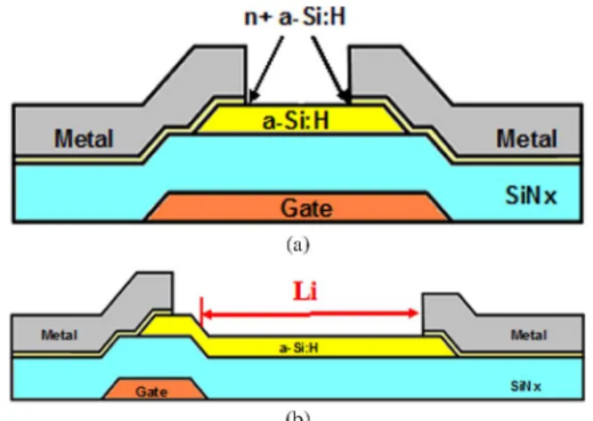
Fig. 1. Cross sections of (a) the conventional and (b) the gap-gate a-Si:H TFT.
the both the front and back light illumination when it is applied in LCD. In this paper, overcoming the above issues, a feasible way of using the gap–gate a-Si:H TFT as the light sensing de-vice in LCD is proposed.
II. DEVICEFABRICATION ANDCHARACTERISTICS
A. Process Flow and Performance of Gap-Gate Type a-Si TFT
The device process flow of the gap-gate type a-Si TFT, which takes advantage of the compatibility to the conventional a-Si TFTs process, is described as followed. Firstly, the gate metal was deposited and patterned on the glass substrates. After the deposition of SiN as gate insulator, shaped a-Si silicon was formed as active layer in a plasma-enhanced chemical vapor deposition (PECVD) system. Subsequently, after the deposi-tion of n+ layer, the source/drain electrodes were formed and defined. Then, the n a-Si:H region between the source–drain electrodes was etched off by a reactive ion etch to make devices with length (L) of 5 m and a gap length (Li). Finally, a passiva-tion layer was used to cap the channel region. The cross secpassiva-tion view of conventional and gap-type structure TFTs are shown in Fig. 1(a), (b), respectively. The only difference between the two device structures is that the gap-type device structure has a gap region between the source–drain metal and the gate metal [8].
Fig. 2(a) and (b) shows the transfer characteristics of the con-ventional a-Si:H TFT and the gap–gate type a-Si:H TFT under front illuminations, respectively. It is obviously seen that the photo-currents of the conventional and gap–gate a-Si:H TFTs in on region are different under various lighting illuminations. Comparing to the conventional a-Si:H TFT, the illuminated on current level of the gap–gate TFT is smaller. Besides, the ratio of light and dark current for the gap-gate a-Si:H TFT is higher, which implies the better resolution of light intensity. For the
Fig. 2. Characteristics of (a) the conventional and (b) the gap-gate a-Si:H TFTs irradiated by different front light intensities.
gap–gate TFT, the photo sensitivities for on and off regions are similar, but as sensing signal, the much larger on current level is preferable.
The gap region in the gap-gate TFT increases the total re-sistance between source and drain, so that the on current of gap-gate TFT is lower than the on current of the conventional TFT. The total resistance can be regarded as the sum of the resistance of the gate channel and gap channel ,
namely, . In the on region, should be
low in the on region, so that the is dominated by . It is consistent with the observation that the illuminated on current of gap-gate TFT differing from the conventional TFT is that it is not changed by the gate voltage. To further confirm the domi-nance of , the photo characteristics of gap–gate TFT oper-ated in on region with different gap lengths Li are examined, as shown in Fig. 3. The drain current is inversely proportional to Li. It implies that the gap region is the sensing area to dominate the illuminated characteristic of gap-gate a-Si:H TFT in the on region. TFT with gap length of 30 m is selected in following discussion for the optimal photo sensitivity.
Fig. 3. Photo-current versus length under various illuminations.
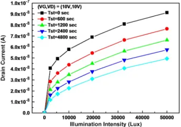
Fig. 4. The behavior of gap-gate a-Si:H TFTs under the stress of 16673 lux front light.
B. Degradation Under Illumination
Illuminated drain current deterioration in thin-film a-Si:H is well known as the SW effect [9]–[12]. Gap-gate a-Si:H TFTs also suffer from the degradation in the photo-current. Fig. 4 shows the curves of current versus illumination intensity for the gap-gate TFT stressed for up to 4800 seconds by a halogen lamp of a continuous front illumination intensity of 13600 Lux. The drain current degradation under illumination stress is obviously observed.
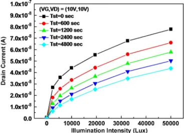
When the gap-gate a-Si:H TFTs are used as sensing devices in TFT LCD, they are irradiated by backlight of display, too. Therefore, the influence of backlight illumination must also be considered. The degradation in the on current of the gap-gate a-Si:H TFT with time under backlight is shown in Fig. 5. For both of Fig. 4 and Fig. 5, it is observed that the degradation trend and level of the illuminated drain current are very similar.
From the discussion in the previous section, the photo effect of gap–gate TFT in the on region is restricted by the high re-sistance of gap region. The same high rere-sistance of gap length makes the current degradation with time, resulting in the same trend for the front and back illuminations. The different degra-dation levels are attributed to the different illuminated intensities and spectrums.
Fig. 5. Behavior of gap–gate a-Si:H TFTs under the stress of 19160 lux back light.
Fig. 6. Drain currents measured with and without backlight illumination after front light stress.
Fig. 6 shows the on current of the gap-gate a-Si:H TFT mea-sured under various front light intensities, with and without the illumination at a fixed backlight intensity of 5070 lux. The with back light is marked as and that without backlight is named as . These currents are measured at drain voltage of 10 V and gate voltage of 20 V after different illuminated stress time (Tst) by the front light. It is observed that the curves of and exhibit parallel shift in the x-axis approx-imately, even for the different stress time. This shift is caused by the backlight of the fixed intensity. It is further observed that the degradation trends under the two conditions are similar.
A new parameter , which is defined as the ratio of
to is plotted against the front light intensity in Fig. 7. As can be seen, the curves of R versus intensity of the front light coincide for various stress time. It implies that we can use this ratio R to be an index for the light sensing, even with the decay in the drain current after long-term illumination. A formula in
the form of is used to best fit the curves in
Fig. 7. Using the fitting curve as a reference, the light intensity can be looked up from the ratio R and the extracted error can be calculated.
Fig. 7. Ratio R with respect to front illumination under front light of 13600 lux for different stress time.
Fig. 8. (a) Measured intensity back traced by parameter R. (b) The error com-parison of with and without calibration under different stress time of 13600 lux front light.
Fig. 8(a) shows the back traced light intensity
for various applied front light intensity . The term represents the identified illumination intensity
mea-sured by a photometer, and the term represents
the measured result according to the correction concept in last paragraph. In ideal case, the slope of the curve in Fig. 8(a) is equal one. Meanwhile, the corresponding errors for those
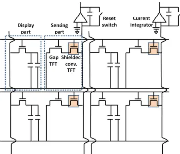
Fig. 9. Proposed front light sensing array circuit using gap-gate TFT.
data extracted from and the drain current after long-term illumination are presented in Fig. 8(b). The error is defined as . In conventional case without calibration, the sensing result is calculated by the de-graded illuminated current according to the initial illuminated characteristic of gap-gate TFT. Therefore, the sensing error without calibration increases with the stress time as shown in Fig. 8(b). In the weak front illumination below 6000 lux, the error of the calibrated case is less than 13%. The large error for the high-intensity light is attributed to the fast degradation during the measurement. Fortunately, such a high intensity is rarely the case in normal usage. The independence of stress time for the ratio provides a way to get around the difficulty in application owing to SW effect, which is to be discussed in the next section.
III. APPLICATION INTFT LCD
A. Proposed Sensing Circuit
The proposed light sensing array circuit including the display and sensing parts is shown in Fig. 9. Because the on–off current ratio for the gap-gate a-Si:H TFT is not very large, in order to restrain the leakage current from the unselected pixels on the same column, a conventional a-Si:H TFT with light shield is connected in series with the gap-gate TFT. The shielded a-Si:H TFT limits the off current of unselected pixel. Meanwhile, the sensing signal is dominated by the dark or illuminated on current of gap-gate TFTs, since it is much smaller than the on current of conventional a-Si:H TFTs.
The proposed circuit does not need the source follower circuit to buffer out the signal because the on current is used to extract the sensing signal [13]. Thus, it occupies less area and a lager aperture ratio can be obtained. Moreover, it avoids the sensing error arisen from the threshold voltage variation of the source follower TFT, since the drain currents of gap-gate TFTs is inde-pendent of gate voltage in the on region, as shown in Fig. 2(b). The error caused by the threshold voltage shift is no more an issue in the proposed circuit.
Fig. 10. The timing scheme of the proposed circuit.
B. Operation in TFT LCD
In order to obtain the proposed ratio R, both and must be acquired. In many advanced TFT LCDs, to elim-inate the motion blur, black frames are inserted between normal frames [14], [15]. These black frames can be implemented by turning of the back light. Taking advantages of this technique, we propose the operation method. The timing scheme for the proposed circuit is shown in Fig. 10. Before each scan line turning on, the reset switch is closed to reset the current inte-grator. In the black frame, for all the pixels in the array can be measured line by line and the values for the whole ma-trix can be stored in a frame memory. In the following normal frame, another matrix values of can be detected and stored with backlight on. Assuming that the front light does not change in these two successive frames, the ratio R for each cor-responding pixel can be calculated and stored by the system. Consequently, the front light intensity can be determined by re-ferring the calculated ratio to the predetermined curve of versus light intensity.
IV. CONCLUSION
It is firstly found that the ratio of the front light-induced currents of the gap-gate a-Si:H TFT with and without backlight illumination is independent of the illumination stress time. This phenomenon gives a way to avoid the issue of SW effect when the gap-gate a-Si:H TFT is used as the light sensor. We propose a simple sensing array circuit and its operation in an array. This method has merits of large signal current level, wide dynamic sensitivity, high pixel aperture ratio, and immunity to threshold voltage shift. It can be easily implemented in TFT LCD since it can be made by the same process with conventional display and the operation is compatible with the TFT LCD application.
REFERENCES
[1] W. den Boer, A. Abileah, P. Green, T. Larsson, S. Robinson, and T. Nguyen, “Active matrix LCD with integrated optical touch screen,” in
SID’03 Dig., 2003, pp. 1494–1497.
[2] A. Abileah, W. den Boer, T. Larsson, T. Baker, S. Robinson, R. Siegel, N. Fickenscher, B. Leback, T. Griffin, and P. Green, “Integrated optical touch panel in a 14.1 AMLCD,” in SID’04 Dig., 2004, pp. 1544–1577.
[3] M. Yamaguchi, Y. Kaneko, and K. Tsutsui, “Two-dimensional contact-type image sensor using amorphous silicon photo-transistor,” Jpn. J.
Appl. Phy., vol. 32, no. 1B, 1993.
[4] T. Hamano, H. Ito, M. Takenouchi, T. Ozawa, M. Fuse, and T. Naka-mura, “Elongate thin-film reader,” U.S. Patent 4 419 696, Dec. 6, 1983. [5] C. Van Berkel and M. J. Powell, “The photosensitivity of amorphous silicon thin film transistors,” J. Non-Crystalline Solids, vol. 77–78, no. 2, pp. 1393–1396, 1985.
Appl. Phys., vol. 51, no. 6, pp. 3262–3268, 1980.
[10] M. Vanecek, A. Poruba, A. Fejfar, and J. Kocka, “Direct measurement of the deep defect density in thin amorphous silicon films with the ab-solute constant photocurrent method,” Jpn.. Soc. Appl. Phys., vol. 78, no. 10, pp. 6203–6210, 1995.
[11] T. Kruger, “On the origin of the Staebler–Wronski effect,” J. Appl.
Phys., vol. 99, no. 6, p. 063509, Mar. 2006.
[12] L. Eglseer, S. Horvat, and H. Kroha, “Study of the long-term behavior of the sensitivity of amorphous silicon photo detectors under illumina-tion,” in Eur. Symp. on Semiconductor Detectors, Nov. 2006, vol. 568, no. 1, pp. 18–21.
[13] M. Hack, A. G. Lewis, and R. H. Bruce, “Timing independent pixel-scale light sensing apparatus,” U.S. Patent 5 153 420, Oct. 6, 1992. [14] H. Pan, X.-F. Feng, and S. Daly, “LCD motion blur modeling and
anal-ysis,” in IEEE Int. Conf. on Image Process., 2005.
[15] S. Hong, B. H. Shin, T.-S. Kim, B. Berkeley, and S. S. Kim, “Advanced method for motion-blur reduction in LCDs,” in SID’05 Dig., 2005, pp. 466–469.
Ya-Hsiang Tai received the B.S. and Ph.D. degrees
in electronic engineering from National Chiao Tung University, Taiwan, in 1990 and 1996, respectively.
He became a member of Industrial Technology Research Institute/Electronics Research & Service Organization and the TFT LCD development as a panel designer. He joined the project of low temperature polycrystalline silicon (LTPS) thin-film transistor (TFT) development in Prime View In-ternational in 2000. In 2001, he joined Toppoly Optoelectronics Corporation, to lead the team of
degree in electro-optical engineering from National Chiao Tung University, Taiwan.
His current research interests include the sensor and applications of a-Si and a-IGZO TFTs.
Hao-Lin Chiu received the B.S. degree in electrophysics from National Chiao
Tung University, Taiwan, in 2004, the M.S. degree in electro-optical engineering in National Chiao Tung University, Taiwan, in 2006, and is currentlyy working toward the Ph.D. degree at the same university.
His current research interests include the sensor and applications of a-Si and a-IGZO TFTs.