quantum dots
V V Ilchenko,
S
D Lin, C P LeeNational Chiao Tung University, 1001 Ta Hsueh Rd., Hsinchu, Taiwan, R.O.C. 0 V Tretyak
Kiev Taras Shevchenko University, 64 Vladimirskaya street, Kiev, Ukraine
Abstract. Deep level capacitance transient spectroscopy was used to obtain the energy level and the capture characteristics of InAs self-assembled quantum dots embedded in GaAs. A specially designed structure was used for the DLTS measurement for enhanced resolution. This structure allows us to detect capacitance relaxation signal from a single layer of quantum dots and to separate this signal from those of the DX centers inside the structure. The DLTS spectra with different filling pulses and different rate windows provide clear information on the energy level and the capture characteristics of the quantum dots.
1. Introduction
Considerable interest has recently been focused on characterization of self-organized quantum dots [l-lo]. In order to develop a new generation of devices such as QD lasers, optical memory elements and resonant - tunneling devices based on quantum dots, it is very important to have a complete understanding of the physical properties of the QDs. To obtain information about energy levels of quantum dots, optical methods such as Photoluminescence (PL) [4-61 are usually used.
Recently, DLTS (Deep Level Transient Spectroscopy) has also been used [ 1- 3,7,9,10]. In principal DLTS method has some advantages over conventional optical methods. The transient capacitance techniques are able not only to detect levels of quantum dots, but also unambiguously to determine their capture parameters.
However, hitherto, investigation of a single layer of QDs in ordinary Schottky-diode structures by means of DLTS has been with difficulties because of small or not clear relaxation signals. The DLTS spectras on QDs reported in the literatures usually dealt with multiple layers of QDs [2,7]. In this paper we describe a new structure, which contains a GaAs-Alo.35Gao.65As heterojunction, for the DLTS investigation of a single layer of QDs. It enables us to obtain very clear and unambiguous DLTS signals of the QDs. Because of the presence of the second potential barrier, which is provided by the GaAs/Alo,uGao,asAs
0-7803-6258-6/00/$10.0002000 EEJ3
_ _ _ _ ~ ~ _ _ _ _ ~
44
heterojunction not far from the QDs, the structure allows us to easily change the extent of filling of the QDs and to obtain the signals.
2. Experiment data and discussion of results.
2.1. Samples and method of study
The samples used for this study were grown by molecular beam epitaxy using a Varian GEN
I1
system. The structure consisted of, starting from the (100) n+-GaAs substrate, a Si-doped n+-GaAs buffer layer, a n+-Al0.3sGa0.6sAs layer (2x 10l8 cm3, 300nm), a n-Alo.35Gao.bsAs layer ( l ~ l O ’ ~ c m ” , 150nm), a 10nm
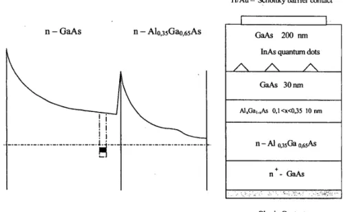
n-type graded A1,Gal.,As layer, a n-GaAs space layer (3.5~10’’ cm”, 30nm), an undoped InAs quantum dot layer (2.6ML), and a n- GaAs layer (n=3.5x10I5 ~ m - ~ , 270nm).The structure and the band diagram are schematically shown in Fig.1. The growth rate of InAs quantum dots was about O.lML/s and the growth temperature was 52OoC. To improve the uniformity of the dot size, we interrupted the In flux for six seconds for every 0.2ML. Afier the layers were grown, TVAu Schottky diodes with a size of 1 . 4 4 ~ 1 0 - ~ c m * were formed for DLTS measurement by standard lithographic technique. The back ohmic contact was formed by alloying In to the n+- GaAs substrate.
The additional GaAs/Alo,3~Gao.~~As heterobarrier undemeath the QDs of this specially designed structure has two purposes: (1) to create conditions under which all QD
TilAu - Schottky barrier contact
InAs quantum dots
Al,Ga,..As 0,1<x<0,35 10 nm
I
IFig. 1 Band diagram of the structure for DLTS measurements at zero offset voltage and layer structure of the quantum dot sample.
states can be completely filled at zero or small negative offset voltages, and (2) to provide a more desirable voltage distribution near the quantum dot layer to facilitate the filling and escaping processes for electrons in the quantum dots during DLTS measurement.
The DLTS measurement was carried out using a MI-401 Megabytec DLTS spectrometer. Low temperature ( at 20K) photoluminescence (PL) spectra were measured using argon laser for excitation. InGaAs detector and Si-PMT were used for light detection. 2.2. Result and discussion
All the DLTS measurements were performed by direct determination of the electron emission rate as a function of temperature from 80 K to 472K in a wide range of time window from s to lo-' s under dark condition. Before each scan, the sample was cooled down under zero bias and the measurements were made during the warm up cycle.
Fig.2 shows the measured DLTS spectra with different filling pulses. The rate window was 3 . 4 ~ lo4 s and the offset voltage was -5.5 V. To vary the average occupation of the dots, the amplitude and the duration of the filling pulses were varied. DLTS signals (curves (1-3) in Fig. 2) from the quantum dots were clearly observed when the positive filling pulses were more than 3 V with different duration of filling pulses. In cases when the filling pulses were smaller and long, wider and more symmetric DLTS signals (curves 4 and 5) were obtained.
These signals were observed in all samples with and without QDs and they had distinctly different physical characteristics very typical for the well-known DX-centers in the Al0.3~Gao.6sAs layer [11,12]. To separate parentage of different peaks we have also prepared a similar structure but without quantum dots. In this case, all the quantum dot peaks completely disappeared. Only the DLTS signal from the DX-centers remained.
0 ' h L - 1 n 0 m - 2 ' Y' , ' c
-
al 0 -3 amplitude (3)- 2.0v (1)- 5.0V (5)- 0 . 5 V -4 -150 200 250 T e m p e r a t u r e ( K )Fig. 2 DLTS spectra taken at a constant offset voltage of -5,5 V and a rate window of 3.4 x lo4 s with different amplitudes of filling pulses. 1000 h 01 Y
::
100 Y h 01 I- x 3 I- (3 CO 10 vs
1-in(
lo9 K-' 5 6 7Fig. 3 Activation plot for DLTS signal from QDs with the 3.0-5.0 V pulse, and from DX-centers obtained with the 0.5 V amplitude of filling pulses.
46
Besides, the signal from the DX-centers could be completely switched off by means of short filling pulses with duration less then 5 x lo-' s because of the relatively small capture cross- section for DX-centers. Fig.2 also shows that the position of the QD's DLTS peak varies with the height of the filling pulses when they are below
5V
and remains about the same when the pulse height is above 5V. This is due to the shift in the energy level caused by the electric field from the offset voltage and the filling pulses.From activation plots of these dependences we determine the emission energies (see Fig.3). The saturation point corresponds to the flat band condition and the measured activation energy gives an energy difference between the quantized level in the dots and the
GaAs
band edge to be 0.4 eV.Because of the excellent resolution of the DLTS spectrum, we were able to measure the capture characteristics of the QDs. The electron capture cross section and the quantum dot concentration were then calculated using the ordinary procedure for DLTS analysis to be 1.07 x lo-'* cm2 and 1 .Ox 10" cm-', respectively. It should be mentioned that the cross section about lo-'' cm2 is much higher than those of commonly observed defects, and it is a good indication of the existence of quantum dots.
Fig.4 shows the dependence of the amplitude DLTS signal on the duration of the filling pulse. The measurement was taken at a constant offset voltage of -5.5 V and a rate of window of
3.4
x lo4 s. The amplitude of the filling pulses was 5.0 V. The capture time can be obtained by fitting this dependence with the following equation [13]t
C(tJ
-
C(t, = CO) = CO exp(-'), (1)tc
where C(t,) is the relaxation signal measured with a pulse width of tp,
C(t,
= 00)is
h U Q v)
5 4
n Y- O Ea
0
10-3
10-4 10-5 10-6 10-7Duration of filling pulse ( sec )
Fig. 4 Dependence of the amplitude of DLTS signal on the duration of the filling pulses. The results of measurements were taken at a constant offset voltage of
25000 20000 h ? v 15000 m > fn C 4-
.-
2
10000-
-J n 5000 047
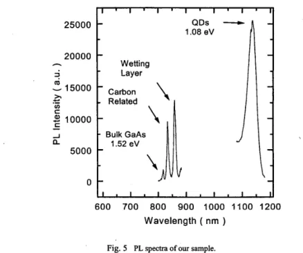
Wetting Layer\
\
Carbon Relatedi
Bulk GaAs 1.52 eV 1.08 eVQDs
7
f 600 700 800 900 1000 1100 1200 Wavelength ( nm )Fig. 5 PL spectra of our sample.
the relaxation signal when the pulse width is infinitely long to saturate the DLTS signal. t,
is the time of capture, which can be expressed as t, = (ovn)-', where cr is the capture cross
section, v is the free electron concentration. The
insert of Fig.4 shows the fitted result. We see that experimental data of short enough duration of pulses followed equation (1) very well. Time of capture of 3x10" s. was calculated on the basis of this result.
We have studied the QDs using an atomic force microscope for as-grown InAs islands. The average lateral size of these islands is around 200
A,
and height of the islands is around 30A. Average concentration is about 1.25 x 10" cm2. These numbers agrees with the concentration determined by DLTS.The samples were characterized by photoluminescence. Fig.5 shows the 20K PL spectra of the samples. The peak related to QDs ground state transition gives an energy of 1.08 eV. Combining the QD emission activation energy of 0.4 eV fiom DLTS with the energy of GaAs related emission (1.52 ev) we can approximately estimate a very small band offset for holes.
is the electron's thermal velocity, n
3. Conclusion
In conclusion, we have used DLTS to characterize a single-layer of self-assembled InAs QDs. The excellent resolution of the DLTS signals was obtained by using a specially designed structure. The electron ground state energy of the quantum dots was unambiguously determined. The density of the QDs, the capture cross section and the
48
capture time were also determined based on the DLTS results. The obtained results agree with those determined by other methods such
as
AFMand
low temperaturePL.
References
Sobolev M M, Kovsh A R, Ustinov V M, Egorov A Yu, Zhukov A E and Musikhin Yu G 1999 Semiconductors 33 157-64
Wang H L, Ning D, Zhu H J, Chen F, Wang H, Wang X D and Feng S L 2000 J. of Crystal Growth 208 107-12
Ghosh S, Kochman B, Singh J and Bhattacharya P 2000 Appl. Phys. Lett. 76 2571-3
Kalevich V K, Tkachuk M N, Le Jeune P, Marie X and Amand T 1999 Phys. Solid State 41
789-92
Yamanaka K, Suzuki K, Ishida S and Arakawa Y 1998 Appl. Phys. Lett. 73 1460-2 Tsai F Y and Lee C P 1998 J. Appl. Phys. 84 2624-7
Walther C, Bollmann J, Kissel H, Kirmse H, Neumann W and Masselink W T 2000 Appl. Phys. Lett. 76 2916-8
Brunkov P N, Suvorova A A, Bert N A, Kovsh A R, Zhukov A E, Egorov A Yu, Ustinov V M,
32 1096-100 Tsatsul’nikov
A F, Ledentsov N N, Kop’ev P S , Eaves L and Main P S 1998 Semiconductors
Anand S, Carlsson N, Pistol M-E, Samuelson L and Seifert W 1995 Appl. Phys. Lett. 67 3016-8
[lo] Anand S, Carlsson N, Pistol M-E, Samuelson L and Seifert W 1998 J. of Appl. Phys. 84 3747-55
[l 11 Grummt G , Piekenhait R and Lehmann L 1990 Solid State Commun. 73 257-63 [12] Mooney P M 1991 Semicond. Sei. Technol. 6 B1-8