IEEE TRANSACTIONS ON COMPUTER-AIDED DESIGN, VOL. 10, NO. 4, APRIL 1991 447
An Integrated CAD System for Algorithm-Specific
IC Design
C. Bernard Shung, Rajeev Jain,
Member, IEEE,Ken Rimey, Edward Wang, Mani B. Srivastava,
Brian C. Richards, Erik Lettang,
Member, IEEE,S.
Khalid Azim,
Member, IEEE,Lars Thon,
Student Member, IEEE,Paul
N.
Hilfinger, Jan M. Rabaey,
Member, IEEE,and Robert W. Brodersen,
Fellow, IEEEAbstract-LAGER is an integrated computer-aided design (CAD) system for algorithm-specific h c g r a c d circuit(1C) design, targeted at applications such as speech processing, image processing, telecommu- nications, and robot control. LAGER provides user interfaces at be- havioral, structural, and physical levels and allows easy integration of new CAD tools. LAGER consists of a behavioral mapper and a silicon assembler. The behavioral mapper maps the behavior onto a parame- terized structure to produce microcode and parameter values. The sil- icon assembler then translates the filled-out structural description into a physical layout and with the aid of simulation tools, the user can fine tune the data path by iterating this process. The silicon assembler can also be used without the behavioral mapper for high sample rate ap- plications. A number of algorithm-specific IC’s designed with LAGER have been fabricated and tested, and as examples, a robot arm con- troller chip and a real-time image segmentation chip will be described.
I. INTRODUCTION
ODERN integrated circuits (IC’s) fall into two groups:
M
commodity IC’s and application-spec@c IC’s (ASIC’s).The turn-around time of ASIC’s is often more important than the area, emphasizing the need for computer-aided design (CAD) tools. Due to their application-specific nature, each de- sign can exploit the special conditions in the particular appli- cation to create an efficient implementation. This paper focuses on ASIC’s that implement real-time computational algorithms called algorithm-speciJlic IC’s. Typical application areas for real-time algorithm-specific IC’s include speech processing, image processing, robot control, computer vision, digital au- dio, and telecommunications. From experience with a number of such IC designs, we find that diverse algorithms can often be implemented with a single, well-designed set of hardware modules and the re-use of these hardware modules greatly re- duces design time.
Two types of architectures are used in designing algorithm- specific IC’s: hardwired architectures and programmable ar-
Manuscnpt received Apnl 19, 1989; revised January 18, 1990. This work was supported by DARPA under Grant N00039-87-C-0182. This paper was recommended by Editor M. R. Lightner.
C. B. Shung is with the Department of Electronics Engineering, National Chiao Tung University, Hsinchu, Taiwan, Republic of China.
R. Jain is with the Department of Electrical Engineering, University of
California at Los Angeles, Los Angeles, CA 90024.
K. Rimey is with the Department of Computer Science, Helsinki Uni- versity of Technology, Helsinki, Finland.
E. Wang, M. B. Srivastava, B. C. Richards, L. Thon, P. N. Hilfinger, J. M. Rabaey, and R. W. Brodersen are with the Department of Electrical Engineering and Computer Science, Electronics Research Laboratory, University of California at Berkeley, Berkeley, CA 94720.
E. Lettang is with the Hewlett Packard Company, San Diego, CA.
S. K. Azim is with AT&T Bell Laboratories, Allentown, PA. IEEE Log Number 9042087.
chitectures. In a hardwired architecture, a dedicated hardware module is allocated for each operation in the data-flow graph of the algorithm; an adder for an add operation, for example. In this way, the abstract data flow in the algorithm is realized by the physical interconnection of the hardware modules. Al- though the data path may be complicated, the control unit is simple because there is no time multiplexing of hardware mod- ules. The speed of the circuit is limited by the speed of the slowest hardware module in the design, but the input of new data (sample rate) can be equal to this value. The main draw- back of hardwired architectures is that they have to be rede- signed for each new algorithm and become less efficient if com- plex decision making is required.
A programmable architecture consists of a carefully chosen set of hardware modules that are time multiplexed under micro- code control according to the algorithm being implemented. The control unit for a programmable architecture is necessarily more complex than that for a hardwired architecture. The speed of the circuit depends on the total number of instruction cycles required to realize the algorithm. Hence, a programmable ar- chitecture can be used in a real-time application only if
sample period circuit cycle time ’
total number of instruction cycles 5
For example, if the circuit runs at 5 MHz and the sample fre- quency is 5 kHz, the number of cycles must be no greater than 1000. Because a single programmable architecture can be used for many applications, it is a good choice when the sample rate permits. On the other hand, high sample rate applications re- quire hardwired architectures because only dedicated hardware modules can provide the required speed.
There are three levels of design descriptions for algorithm- specific IC’s, namely, behavioral, structural, and physical. A behavioral representation specifies the algorithm that the chip implements, which may take the form of a program or a signal- flow graph. A structural representation specifies the chip archi- tecture in terms of hardware modules and their logical connec- tions. A physical representation specifies the chip layout.
This paper describes LAGER, an integrated CAD system for automatic generation-from high-level (behavioral or struc- tural) user specifications-of chip layouts for hardwired or pro- grammable architectural implementations of algorithm-specific IC’s. In Section I1 we discuss design strategies of LAGER and compare them with previous work. In Sections 111 and IV we describe the two parts of LAGER: the behavioral mapper and the silicon assembler, respectively. We will show several de- sign examples in Section V .
448 IEEE TRANSACTIONS ON COMPUTER-AIDED DESIGN, VOL. 10, NO. 4, APRIL 1991 11. DESIGN STRATEGIES FOR ALGORITHM-SPECIFIC IC’s
In Section 11-2.1, we first review the development of some
existing CAD tools for algorithm-specific IC’s, and motivate the need for a new design environment. In Section 11-2.2, we
will describe the new problems that are solved, and the basic design methodology adopted in LAGER.
2 . 1 . Background
2. I . I . Behavioral Description: Many behavioral descrip-
tions have been proposed for design capture at the behavioral level. A frequency-domain specification is used [l], which al-
lows the users to specify filter parameters such as the passband ripple, stopband ripple, and stopband attenuation, etc. This ap- proach offers the highest level description; the user only spec- ifies what he needs rather than how to do it. However, the ap- plication of this approach is limited to digital filter circuits.
Most algorithm-specific IC applications can be described by
signal-$ow diagrams. Hence, an applicative programming lan- guage [2], [3] is a natural choice for algorithm specification. It
is also inherently parallel, so the same applicative language pro- gram can serve both a uniprocessor or a multiprocessor reali- zation. On the other hand, procedural programming languages such as Pascal [4] or ISPS [5] have also been adopted, which
provide a mechanism for describing the control flow of the al- gorithm. For high-level procedural languages, existing compi- lers can be exploited for algorithm simulation. Although inef- ficient for direct encoding of algorithms, ISPS is very useful for machine description for its low-level mechanisms such as bit operations and timing contol. In LAGER, both an applicative (Silage [2]) and a “C-like” procedural language (RL) are pro-
vided. These languages will be described in Section 111. 2.1.2. Behavioral Synthesis: Behavioral synthesis [6], [7]- [ 1 11 attempts to generate a structural description from a behav-
ioral description directly. Due to the vast amount of design al- ternatives inherent in the behavioral synthesis systems, some search pruning is mandatory. In most systems, high-level de- cisions-bus structure [7], pipelined versus nonpipelined archi-
tectures [SI, lumped ALU versus distributed functional mod-
ules [ l l ] , [12]-are predetermined to make the problem tract-
able. These a priori design decisions, however, are usually too restrictive to deliver efficient designs. Also, because the end product of most behavioral synthesis research is a block dia- gram instead of a layout, its performance evaluation often lacks practical considerations. For example, it has been found [13]
that the data-path partitioning has a significant impact on the final layout area. In algorithm-specific IC designs, there are many additional issues that are more important than the effi- ciency of the data-path logic. For instance, it was pointed out
[ 141 that I/O compatibility between the raster-scan format of
the camera and an image processing circuit is essential to achieve real-time image processing. It is an open question as how to incorporate these issues in the behavioral synthesis framework.
For these reasons, LAGER supports user specification of the data paths and then generates the rest of the design from a be- havioral description. Support for behavioral synthesis with ap- propriate optimization criteria for our application focus is planned for the future [ 131.
2.1.3. Silicon Compilation into A Fixed Architecture: There have been a number of silicon compilers [I], [ 121, [ 151-[20]
that can translate the high-level description to layout for a fixed
architecture. In [ 11, [15], [16], bit-serial architectures were
used, in which the throughput rate of the chip was limited by the data wordlength in addition to the clock speed. The user interface in FIRST [ 151 is at the structural level so that the user has to translate the algorithm to a bit-serial architecture man- ually. Moreover, a hardwired floorplan is used which can result in a substantially larger chip area than that of a manual design. The INPACT compiler [16] has a higher level interface that
allows the algorithm to be specified in a programming lan- guage, and performs some optimization on the floorplan. Ca- thedral-I [ l ] provides a high-level interface and performs sev-
eral optimizations at the algorithmic, architectural, and floorplan level; however, the user interface and optimizations are pri- marily applicable to digital filter algorithms.
A second class of compilers uses microprogrammed bit-par- allel architectures. While the achievable throughput rate is usu- ally similar to that of bit-serial architectures, they provide greater flexibility in the algorithmic operations and the I/O in- terfaces. Examples of these compilers are given in [12], [17]- [20]. In [17], a register-transfer language is provided for de-
scribing the algorithm and a fixed floorplan strategy is used. In
[12], an interface to a high-level applicative language [2] is pro-
vided and symbolic layout techniques are employed for optim- izing the chip area.
The drawbacks with these compilers are that the target ar- chitecture uses a predefined data path and architectural modifi- cation by the user is very difficult. Furthermore, the layout gen- eration techniques are fixed and cannot be influenced by the user. The fixed target architecture and predefined floorplanning limit the application of the above compilers to low throughput rate applications, typically with data rates below 1 MHz. In addition, the algorithmic operations that can be handled are lim- ited by the predefined hardware modules that the compiler can handle.
2.2. Overview of LAGER
2.2.1. Motivation: To expand the kind of algorithms that can
be handled, as well as to attack applications with high data rates
(10 MHz and above), LAGER allows the user to modify or
even completely specify the target architecture. In contrast to the ‘ ‘fixed-architecture silicon compiler” approach, a structural interface is established in LAGER. The user can use or modify predefined architectures in the library, or design a new target architecture through the structural interface.
To provide this flexibility, the LAGER environment is built from two distinct subsystems: 1 ) a behavioral mapper and 2 ) a
silicon assembler. In contrast to the “behavioral synthesis” ap- proach which attempts to synthesize the optimum architecture from a behavioral description, the LAGER behavioral mapper maps the behavioral description into a user-defined architec- ture. This approach allows the user to fine tune the target ar- chitecture by iteration to achieve desired performance with ac- ceptable chip area.
The separation of the behavioral mapper and the silicon as- sembler has two more advantages. First, for high-speed appli- cations in which hardwired architectures are often more appro- priate, the silicon assembler can be used independently to generate a layout from a user-defined hardwired architecture. Second, the LAGER silicon assembler can be a backend of the emerging behavioral synthesis programs (as in [ 131) to provide a means for automatic layout generation as well as feedback for performance and chip area evaluation.
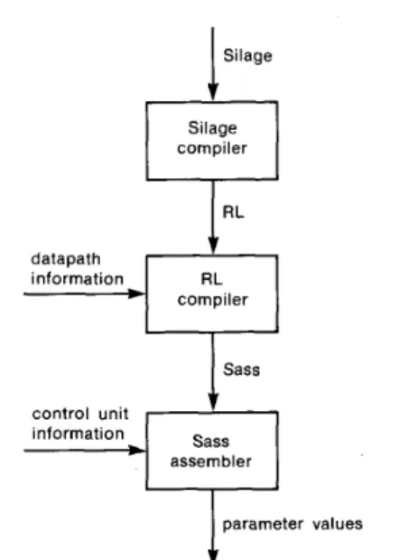
SHUNG et al.: CAD SYSTEM FOR IC DESIGN 449 behavioral description
I
Silage behavioral mapping structural description parameter physical descriptionFig. 1. Block diagram of LAGER.
Silage compiler
I
R L datapath information compiler control unit information assembler2.2.2. Behavioral Mapper and Silicon Assembler: LAGER consists of a behavioral mapper and a silicon assembler, a block diagram of which is shown in Fig. 1. The structural description in LAGER is parameterized to facilitate the reuse of hardware modules or architectures. The silicon assembler requires both a structural description and associated parameter values to gen- erate the layout. Examples of parameters are: the wordlength of the data path and the contents of the microcode PLA. The behavioral mapper maps a behavioral description onto a user- specified structural design by generating the appropriate param- eter values.
The task of the behavioral mapper is similar to that of a high- level language compiler that generates microcode. This micro- code is essentially one of the parameter values of the program- mable architecture. The behavioral mapper can be retargeted to different structural descriptions. This is essential to the design cycle in which the architecture is tailored to the application: first, the algorithm is mapped to an existing architecture. Then, if the result is unsatisfactory, the architecture is modified and the algorithm is mapped to the new architecture. This process is iterated until a satisfactory architecture is obtained. The usual cause of dissatisfaction with an architecture is that frequently used instructions are not directly implemented. This situation is easily recognized from a histogram of instruction usage.
The LAGER silicon assembler integrates a number of layout generation and simulation tools under a user interface called the
design manager. All communications among tools is through a common data base with procedural interfaces for data storage, retrieval, and modification. Integrating the tools is easy because they follow an agreed upon data base policy. The design man- ager builds the data base from the structural description. There are extensive cell libraries (of leaf cells and parameterized mod- ules) which can accommodate various layout styles in the same chip design. New modules are added to the library by providing structural descriptions; new cells are added by providing sim- ulation models and layouts.
111. BEHAVIORAL
MAPPING
LAGER can work from a behavioral (architecture indepen- dent) description of the algorithm. This description is mapped into parameter values, which completes the parameterized structural description, and in turn becomes the input to the sil- icon assembler.
parameter values
Fig. 2. Block diagram of the behavioral mapper. The user can use any of the three languages: Silage, RL, and Sass to encode the algorithm. Trans- lators are also provided. Some require data path or control unit information
for retargetable translation.
Fig. 2 shows a block diagram of the behavioral mapper. We
employ three independent input languages. Silage is a data-flow language with very high-level constructs suited to the intended ASIC applications. RL is a variant of C, a procedural language with comparatively primitive features. Sass is an assembly lan- guage. The system supports all three languages equally; the user has the freedom to choose the input style most suited to his needs. Fig. 3 shows a simple infinite impulse response (IIR) filter, defined by the recurrence
3 1
' 4 4
x. = - x i - ,
+
-
inidescribed in the three languages. Each language has an accom- panying translator that maps a program into the next lower level. The languages and their translators are described in Sections Section 111-3.1 describes the Kappa model of processor ar- chitectures. RL and Sass can be used for any architectures that fit the Kappa model. Silage is designed to be free of architec- tural bias, but the current Silage to RL translator is tailored to the RL compiler, and therefore, to the Kappa model.
111-3.2-111-3.4.
3. I . The Kappa Architecture Model
Kappa [21] is a processor architecture model that has served well as a prototype for customization. A more detailed descrip- tion of Kappa is given in Section V-5.1. The Kappa model con-
tains a control unit and a number of data paths. The control unit generates micro-instructions to control the data paths, and the data paths feed the status signals (e.g., sign bits) back to the control unit, which are used as input for state transition in the control unit. The control unit can provide all control functions independent of the data paths. Some unique control mechanisms are also incorporated, as it has been found [21] that an ineffi-
cient control unit is the speed bottleneck in some applications. For example, for looping and more complex decision making,
450 IEEE TRANSACTIONS ON COMPUTER-AIDED DESIGN, VOL. IO, NO. 4, APRIL 1991 fnnc main(in: fix<8>): fix<8> =
begin
end ;
return = (3/4) * return01 + (1/4) * in; (a) f i x y ; m a i n 0 I y = (3/4) * y + (1/4) * (fix) in(); out ( y ) i 1 (b) (ram y) (cfsm (0 0 nil (goto 0))) (dp-word-size 8 )
(rom (0 ((addr y) (mor=mem) (r*=rbus 0) (rbus=ioport) (ioport=sxtport 0)) ((acc=abus) (abus=mor))
((abus=mor) (nosat) (acc=sum) (bbus=acc>r 1 ) )
((acc=bbus) (bbus=acc>* 1))
((acc=bbus) (bbus=mbus) (mbus=r* 0) (rr=rbus 0) (rbus=acc)) ((acc=bbus) (mor=nbus) (mbus=rr 0) (bbus-acc>* 2 ) )
((bbus=acc>* 0) (abus=mor) (acc=sum))
((mbus=acc) (ioport=mbubus) (axtport=ioport 0 ) (addr y ) (mem=mbus)))) (c)
Fig. 3 . (a) The IIR filter described in Silage. (b) The IIR filter described in RL. (c) The IIR filter described in Sass.
the Kappa control unit provides a multiway jump/call/return ca-
pability.
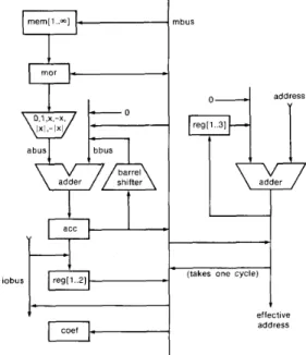
An example of a processor data path that fits the Kappa model is shown in Fig. 4. A pipeline delay of one instruction cycle is associated with every register (mor, acc and coef) and register bank in the figure; these delays include those of the functional units. If the individual functional units are understood, the dia- gram completely defines how they work together-every appar- ent, meaningful combination of actions is possible when the instruction word is fully horizontal. A horizontal instruction word is just a vector of control signals with little or no restric- tive encoding.
Kappa is irregular, meaning that its data path topology can be chosen to suit the usage in a particular program (e.g., a robot arm controller) rather than to conform to the expectations of modem compilers. The alternative would be exemplified by an architecture in which all intermediate results are stored in a large, multiported register bank. An irregular data path is smaller, faster, more tunable, and hence, more appropriate for inclusion in an ASIC. The problems that irregularity poses for retargetable compilers are minimized by the use of a fully hor- izontal instruction word.
The behavioral mapper generates horizontal microcode for the user-defined data path from a behavioral description. The three languages used in the behavioral mapping part of LAGER, Silage, RL, and Sass are described in the following sections.
3.2. Silage
Silage is a high-level language optimized for specifying “sig- nal processing like” algorithms. As such, its design emphasizes expressiveness over details of implementation, by providing the programmer with convenient data types and operations and hid- ing from him quirks of the actual hardware. We will give an overview of the language and its compiler in this section. More detailed descriptions can be found elsewhere [2], [22]. The
‘‘Silage Reference Manual” [23] specifies the language in full. 3.2.1. The Silage Language: Silage is a data-flow language that operates on streams of values. As in all data-flow lan-
lobus
P
reg[l..z]4-
~~ coef Ibus address reg11 ..3]4
(takes one cycle)effective address
Fig. 4. A data-path example that fits the Kappa model.
guages, a Silage program corresponds to a data-flow graph-a directed graph with operations performed by vertices and values carried on edges. A subtraction node, for example, combines two streams of numbers to produce a difference stream. A pro- gram graph accepts input streams, combines and alters them as they flow through the graph, to produce the output streams. This model of computation is natural for our intended applications. For example, real-time control typically takes time-sampled in- put streams from sensors to produce control signals. Digital sig- nal processing (DSP) operates on streams of digitized signal samples, and a form of dataflow graph is already commonly used to express DSP algorithms. In addition to the usual arith- metic functions, Silage provides some common DSP opera- tions: delaying a stream ( Z - ’ ), taking a substream (decima- tion), and taking the union of streams (interpolation).
The textual Silage program is a set of equations that defines output variables in terms of input variables. Each equation de- fines a single variable to be an expression on other variables. Each variable is defined exactly once, following the single as- signment rule of most dataflow languages. Thus the right-hand side of each definition corresponds to an expression tree; con- necting the trees by linking variable definitions to uses produces the program graph.
Variables can be subscripted in the usual way. The iterated
dejinition provides a general way to operate on subscripted variables. The iterator can specify both parallel and sequential computation. The only difference is in the dependence (or lack of dependence) between iterations. The example in Fig. 3(a) computes an output stream x i (called return in the code), which equals 3 / 4 times the previous sample (return @1, using the delay operator @ ) plus 1 /4 times the current value of in.
Structural preferences can be expressed by the pragma direc- tives [2]. For example, in the case when the number of parallel
processing elements is less than the number of independent expressions that can be computed simultaneously, we can use
SHUNG et a l . : CAD SYSTEM FOR IC DESIGN 45 I to indicate that the expression Expr should be computed on pro-
cessor element
K.
3 . 2 . 2 . The Silage Compiler: The current Silage compiler translates Silage programs into RL to run on a single micro- coded processor. The main difficulties are in converting the unique features of Silage into the conventional operations sup- ported by RL. These include modeling data-flow semantics in a procedural language and building the data structures for streams in terms of primitive data types. Central to a good im- plementation is the conversion of repetition in the data-flow graph into efficient program loops. We call this loop folding.
Repetition can come from iterated definitions, delay queue operations, and interpolated data streams. The loop folder pro- cesses the input program in data-flow graph form, converting repetitive connected subgraphs into loops. The algorithm first finds candidate loops by graph traversal, then creates loop bod- ies that are graph fragments parameterized on the loop indexes. Loop folding typically consumes half of the total compilation time, but because it operates on the iterator-expanded graph, its running time can be exponential on the size of the input pro- gram. It is, however, both simpler and more powerful than the alternative approach that infers iteration dependency on the original iterated definitions by analyzing variable index expres- sions. The basic loop folder is general enough to handle all three sources of repetition. In particular, the copy operation needed to implement delay queues without special hardware support can often be merged into other program loops.
3.3. RL
The task of the RL compiler is to generate a control program for a processor of specified structure. The compiler must meet a pair of conflicting goals. On the one hand, it must be easy to retarget. The user should be able to evaluate a proposed change in processor structure by retargeting the compiler and then re- compiling the program. On the other hand, the compiler must generate good code for diverse, irregular architectures.
We only give a brief overview of the RL compiler here. Ri- mey and Hilfinger describe, in more detail, the overall compiler
[24] and the original code-generation techniques that it uses 3.3.1. n e RL Language: The inputs to the RL compiler are a source program, written in the RL language, and a machine description. Both are provided by the user, although he will usually use or modify previously specified machine descrip- tions.
The RL language is an approximate subset of C. It incorpo- rates two major extensions: fixed-point types and register classes. Fixed-point types provide the programmer with con- venient notation for fixed-point constants and arithmetic. Reg- ister classes, which generalize C register declarations, enable the programmer to suggest storage locations for critical vari- ables.
3.3.2. The Machine Description: A machine description consists of
r251.
declarations of buses, latches, registers, and register banks; a list of simple register-transfers (e.g., abus --* Q C C ) de-
fining the topology of the data path;
a list of functional register-transfers (e.g., abus
+
bbus --t a c c ) representing capabilities of the functional units.The compiler automatically uses simple transfers to chain to- gether functional transfers. It selects from instances of a func-
tional unit when there is more than one. It allows the user to declare register-transfers to be incompatible, as is necessary when the incompatibility is not apparent from a conflict in bus usage.
3.3.3. The
RL
Compiler: The compiler consists of two parts. The front end translates the program into successive straight- line segments of code, expressed in an intermediate language. Then, for each straightline segment, the backend selects regis- ter-transfers and packs them into instruction words.In addition to routine tasks and simple optimizations, the front end performs two optimizations that are particularly important for Kappa model architectures. First, when no parallel multi- plier is provided, it reduces multiplications by constants into minimal sequences of shifts, adds, and subtracts. Second, it co- alesces branches to utilize Kappa’s multiway jump/call/retum. Most of the effort in developing the RL compiler has gone into the algorithms in the backend. The usual approach to gen- erating horizontal code is to first generate loose sequences of register-transfers and then pack these tightly into a small num- ber of instructions through compaction [26]. Our approach is to
integrate register-transfer selection and local compaction into local scheduling. This creates the opportunity to perform a lazy routing of intermediate results between functional units, choos- ing appropriate sequences of simple register-transfers late in the scheduling process when more of the schedule is known. For Kappa model architectures, scheduling with lazy data rout- ing is profitable, but also difficult. The compiler must take care that all feasible routes for a live result are not by chance closed off. A network flow algorithm that performs this test efficiently has been developed [25].
The RL compiler is written in Lisp and compiles approxi- mately one line per second. It has been used to compile pro- grams several hundred lines in length. Making modifications to the machine description has proven to be easy; for evaluating their impact on performance, the compiler has proven to be more reliable than intuition.
3.4. sass
Sass is an assembly-level language. A Sass program consists of symbolic microcode and definitions of the other parameters for a Kappa processor. The body of a Sass program has two parts: straightline code blocks and control flow information. A straightline code block is a sequence of micro-instructions, un- interrupted by branches. Each micro-instruction consists of a number of micro-operations, which perform arithmetic, logic, and addressing functions. Sass programs also define additional parameter values of the processor. For example, the width of the data path is ordinarily specified this way.
In Fig. 3(c), we show a Sass program for a IIR filter. It con- sist of a number of Lisp s-expressions. The expression (ram y ) describes that one local variable, y , is stored in RAM. The
expression (cfsm
. .
a) declares the control flow among thestraightline code blocks. In this case there is only one code block. The expression (dp-word-size 8 ) indicates the width of the data path is 8. Finally the expression ( r o m
-
* ) defines allthe straightline code blocks. In Fig. 3(c) the code block consists of 8 micro-instructions, which have 6, 2, 4 , 2, 5, 4, 3, 5 mi- cro-operations, respectively.
The Sass assembler passes some of the parameter values to the output unmodified; it uses the rest to generate the control unit, which is its main task. Since the Kappa architecture can be customized, a machine description is also needed as input
(Fig. 2). The machine description specifies the control signals and hardware resources used by each micro-operation. The Sass assembler uses it to assemble data-path instructions into binary microcode, and to check for resource conflict errors between micro-operations
.
The Sass assembler's main task is to output a specification (in the form of parameter values) for a Kappa control unit. The control unit includes a read-only control store containing the assembled microcode blocks and a state machine that controls transitions between the blocks. The specification also contains parameter values such as the width of the program counter and the depth of the stack. Some components are not always nec- essary. For example, setting the depth to zero discards the stack in the resultant silicon implementation.
The sample rate of the application that can be achieved using the behavioral mapper depends on the resulting number of in- struction cycles, assuming a fixed circuit speed. The user has the freedom to modify the data path and iterate the process for speed optimization. After this is done? the parameter values and control unit specification generated by the behavioral mapper are sent to the silicon assembler for layout generation.
IV. THE SILICON ASSEMBLER
The task of the silicon assembler is to generate the chip lay- out starting from a parameterized description of the chip archi- tecture. Separating the silicon assembler from the behavior mapper allows the user to change the architecture directly and, furthermore, allows the silicon assembly tools to be used in conjunction with other high-level architecture synthesis aids.
A major goal in developing the silicon assembler was to han- dle arbitrary architectures and to create an environment for quick iteration on different architectural alternatives. A second goal was to allow the re-use of parameterized cells so that a mini- mum effort is required to design new cells. Thirdly, based on circuit design expertise, it was found that it was essential to allow different layout styles to be combined to achieve higher design quality.
To achieve these goals a design management tool [27] was developed. The task of this tool is to automate the layout gen- eration procedure for any architectural description and serve as the user-interface to the silicon assembler. This also shortens the learning curve for the designer to use the silicon assembler since only one tool is seen by the user. The design manager tool in LAGER called DMoct is described in Section IV-4.1. Sec- tions IV-4.2-IV-4.3 describe the layout generation tools cur- rently interfaced to DMoct.
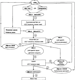
4. I . The Design Manager: DMoct
Fig. 5 illustrates the design methodology followed by DMoct. The input to DMoct is a parameterized hierarchial description of the chip architkcture. For a given set of parameter values, DMoct generates the chip layout. DMoct uses the OCT data- base system [28] to store all design data, which has the advan- tages that it provides a procedural interface for CAD tools and the data representation can be defined by the application. Three OCT representations have been defined for the silicon assem- bler: a) structure-master view; b) structure-instance view; c)
physical view. Details of these views are given in the follow- ing.
The structural description at a given level of the hierarchy can be described textually using structural description language (SDL), which is illustrated in Fig. 6, or graphically using a
I Y
. _.
"Ct
-
generator prqram)
w
Fig. 5 . Design methodology of the LAGER silicon assembler. Items in
ellipse are tools. Items in box are files. Numbers in circle correspond to the 8 design steps.
schematic entry by VEM [28]. In addition to nets, subcells and terminals declared in conventional netlist and hardware descrip- tions, unique features of SDL are: 1) for each cell the tools required to generate the layout are declared; 2) all nets can be parameterized; and 3) each cell in the hierarchy can inherit pa- rameter values from its parent. Thus all cell and net parameter values can be declared as arbitrary functions of a unique set of parameters for the chip (the root cell), typically the algorithm parameters. This allows the user to quickly generate different versions of the chip for different algorithm parameter values without having to change the architectural description.
The operations of DMoct and its associated utilities are de- scribed below.
Step I: Master creation: DMoct parses the SDL files and stores the architecture as a structure-master view in OCT, which can also be created graphically with a schematic entry. This view is an OCT representation of the information shown in Fig. 6.
Step 2: Instance generation: DMoct traverses the design hi- erarchy in a top-down depth-first manner and generates the ac- tual instances. At each level it evaluates the child cell param- eters from the parent cell parameter values. This parameter evaluation mechanism allows a more powerful parameterization compared to pop-up forms used in some commercial CAD sys- tems. The instances are stored in the OCT database as a struc-
ture-instance view. The structure-instance view is used as the common input to all the layout generation tools.
Step 3: Structure processing: Prior to layout generation,
DMoct allows the structure-instance view to be modified by a special class of programs called structure-processors. An ex- ample of a structure-processor is a bit-slice data path processor (Section IV-4.2) that modifies the cell and net information in the structure-instance view to allow a more optimal routing by the layout generation tools.
SHUNG et al.: CAD SYSTEM FOR IC DESIGN 453 parametername
>
k7zGl7,
me, parameter, parameter value’parameter value
-
constant OR function of of subcell, net, terminal-
parent cell parameters Fig. 6 . Syntax diagram of the structural descriptional language (SDL).Step 4: Functional simulation: Assuming that parameter- ized simulation models exist for the leaf cells in the hierarchy (which are usually the library cells). A utility called DMpost is then used to generate a simulation input for the entire design for the simulator THOR [29]. Based on simulation results, the designer can modify the SDL files or parameter values and re- run the simulation. When simulation results are satisfactory, layout generation can proceed.
Step 5: Layout generation: In this step, DMoct traverses the cell hierarchy in the structure-instance view in a top-down depth-first manner. When DMoct reaches a leaf node, it re- curses back up the hierarchy and executes the layout generator program specified for each cell. By policy each layout generator reads its input information about the cell from the structure- instance view and stores the information about the layout as a physical view. If the physical view exists for a cell and is more recent than the corresponding structure-instance view, the lay- out is not generated. This avoids regeneration of cells that are not affected by design iteration.
Step 6: VerBcation: A verification tool DMverify is pro-
vided to check for isomorphism between the schematic repre- sented in the structure-instance view and the hierarchial sche- matic extracted from the physical view. In contrast to conventional netlist verification tools, this program compares the cell hierarchy and connectivity (not transistor or gate level). The inherent assumption here is that at the lowest level, the cells were designed by hand and have been fully debugged using circuit simulation and test chips. The uniform policy imposed on all tools by the structure-instance and physical views takes the guesswork out of the netlist verification so that time con- suming signature analysis and logic extraction procedures can be avoided.
Step 7: Performance estimation: The chip performance de- pends on the performance of the cell library. Currently, a MOSIS rev-6 scalable CMOS library is integrated, allowing clock rates in the region of 20-25 MHz in a 2-pm process. The library provides various data and clock buffering cells so that performance is relatively independent of the place and route
tools if appropriate buffer cells are used. The choice of buffer cells is not yet automated. The chip performance can be esti- mated based on SPICE characterization of the library cells and an estimation of the critical path. Alternatively, the simulator IRISM [30] can be used in the linear mode to obtain perfor- mance estimations.
Step 8: Maskfile generation: When the final layout is ac-
ceptable, mask files can be generated from the OCT physical view.
It is important to note that to perform all the above steps the user only interacts with DMoct and its associated utilities. The designer can rapidly iterate on the design and explore different architectural alternatives by simply changing the schematics and parameter values and rerunning DMoct. The design times for silicon assembly with DMoct are application dependent; some data are given in Section V-5.3.
The LAGER silicon assembler is cell based. The cell library contains parameterized modules and leaf cells. New modules can be added to the library by providing structural descriptions; new leaf cells can be added to the library by providing simu- lation models and layouts. Re-using parameterized modules and leaf cells has proven to be an important factor in improving the productivity.
A new layout generator, structure processor or simulator can be integrated in the silicon assembler by following the policy defined by DMoct. This involves writing procedures to read, write or modify the three OCT views. For information the reader is referred to [28], [31]. Integrating a new tool or cell does not require any modification of the user interface provided by DMoct or of the interface between DMoct and the OCT data- base. This capability is an important feature in creating an open framework for tool integration.
A prototype of the design manager was previously developed using the Flavors package in FranzLisp to implement the data base [32]. This was motivated by the facilities of parameter declaration and evaluation, and the ease of prototyping offered by Lisp, and the advantage of object-oriented paradigm for tool integration offered by Flavors. However, this version was too
454 IEEE TRANSACTIONS ON COMPUTER-AIDED DESIGN, VOL. 10, NO. 4, APRIL 1991
slow to permit efficient design iteration and was less portable than the C-based OCT data base. Also, unlike OCT, which maintains the structure-master, structure-instance, and physical views as disk files, the Flavors-based implementation keeps all design information in the process memory, which limits the de- sign size.
4.2. Layout Generation Tools
While the CAD framework supported by DMoct allows any tool to be integrated so long as it fits the methodology described above, currently, a set of four layout generators are interfaced to the framework which support various design styles required in algorithm-specific IC's. These are described in the follow- ing.
4 . 2 . I . Tiler for Macrocell Layout Generation: TimLager:
TimLager is a general purpose macrocell layout generator that is used for bit-sliced modules such as adders, registers, multi- plexers as well as array-based modules such as RAMS'S, PLA's, and ROM's. It assembles the layout for the macrocell from hand designed leafcells by abutment. This requires the leafcells to be pitch-matched and avoids the use of routing in macrocell gen- eration.
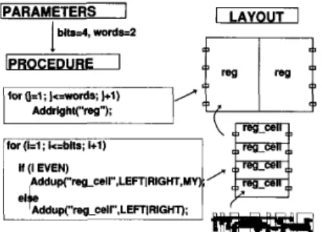
For each macrocell, TimLager requires a set of leafcell lay- outs, and a tiling procedure that describes how the marocell is constructed from the leafcells as a function of the macrocell parameters. The procedure is written using the C language. To allow rapid creation of tiling procedures for new macrocells TimLager provides two tiling functions Addright ( ) and
Addup( ) (Fig. 7). The full capability of C can be exploited for parameterizing the layout. Hierarchical tiling can be per- formed using subroutines. This allows greater flexibility than the personality matrix approach traditionally used in tiling.
Each tiling function has a set of 20 optional arguments that allows geometric transformation on the cell to be placed. The arguments also allow several bookkeeping operations to be au- tomated, such as the naming of terminals. Thus the cell termi- nals as defined in the library can be changed arbitrarily to names more pertinent to a given design. The optional argliments also provide a stretching mechanism that can be used to pitch-match one macrocell to another as well as a mechanism for adding metal feedthrough lines in between cells. These options can be exploited for optimization of a higher level cell (e.g., a data path) constructed from several macrocells generated by Tim- Lager.
The tiling procedure for each macrocell is compiled and stored in the library along with associated leafcell layouts. At runtime TimLager dynamically links the required procedure and exe- cutes it. The parameter values are read from the structure-in- stance view and a physical view is generated for the macrocell layout.
4 . 2 . 2 . Random Logic Macrocells Using Standard Cells: Stdcell: Stdcell provides an interface to a standard cell place and route tool, Wove [28], to generate standard cell modules for a given logic schematic. Wolfe in turn uses the Timber-
WolfsC [33] standard cell placement program and the YACR [34] channel router. The standard cell modules can also be gen- erated from a high-level logic description (see Section IV-4.3.3). Stdcell directly reads the structure-instance view to obtain the logic schematic and generates a physical view for the layout.
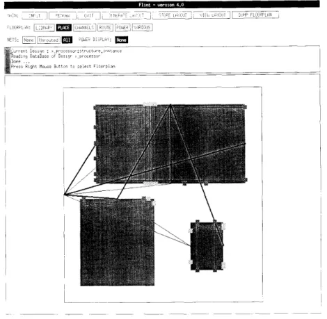
4 . 2 . 3 . Macrocell Place and Route Tool: Flint: Higher level cells can be constructed with Flint [35] from the macrocells generated by TimLager or Stdcell (or any other macrocell gen-
IPARAMETERS
I
1
LAYOUTI
I I 1
fw lJ=l;]<.words; ]+1) Addrlght("reg");
Fig. 7. Tiling procedure used in TimLager. In this example, leafcell reg- cell is abutted vertically by addup( ) calls to form reg, which is abutted horizontally by addright( ) calls to form the module. The module has 2
parameters: bits and words.
erator that produces OCT physical views). Flint supports three floorplan definition alternatives: 1) interactive-graphical (Fig. 8), 2) interactive-textual using a floorplan description language (FDL), or 3) automatic. An automatically generated floorplan
can be further refined using the interactive modes. A floorplan definition contains the relative placement of the macrocells, the definition of the channel areas, and the specification of the global routes for signal, power, ground, and clock nets. In order to make the global routing process tractable in an interactive mode, Flint clusters groups of nets in so called cables (Fig. 8). A cable is a set of nets which have identical sources and desti- nations.
The automatic mode is based on min-cut and slicing. This technique has the advantage that a realizable channel structure is automatically obtained. The placement is then further refined using a modification of Stockmeyer's algorithm [36], an effi- cient tree-traversal method which determines the optimal ori- entation of each macrocell. The global routing is based on Dijk- stra's [37] shortest path algorithm. The use of the cable concept mentioned above increases the efficiency of this phase of the floorplanning process. Finally, the global routes of power and clock nets are determined using an approximation technique for the Steiner tree problem [38]. Flint does not build the power and ground network as a single tree, but rather as a "forest of trees." In fact, it is not necessary to have a connected power network at every level of the chip hierarchy. All the above rou- tines are extremely efficient and complete in less than a minute CPU time for complex examples (up to 20 macrocells and 1000 nets) on a SUN 3/60.
Given the floorplan, Flint carries out all other steps automat- ically including channel routing, power/ground/clock routing, absolute placement, and creation of terminals on the top level cell (interface for the next higher level in the hierarchy). De- tailed routing in Flint is performed by a completely gridless channel router. Although the router is a variant of the classical left-right router, it has some features which distinguish it from other routers. First, it routes signal, power, and ground nets together using a priority scheme, which gives special priority to more sensitive nets such as power and ground. Secondly, it automatically sizes the power and ground nets, using terminal current information if it is available, or else it is based on a saturating weighted sum of the connecting terminal widths. Fi- nally, it supports three layer routing, which is essential when high density routing is necessary as in the case of bit-sliced data paths.
4.2.4. Pad frame generation and routing: Padroute: The creation of a pad frame and routing of signals from the core of
the chip t o the pad frame is d o n e bb a specialized tool called
Pndrourr [391. If the terminals on one side of the core connect only to pads o n the same side of the pad frame. a simple channel router can b e used. H o w e v e r , in practice. this is often not the case and hence. a special ring router is necessary.
T h c ring routing algorithm is a modified channel routing al- gorithm. which allows Podroute to route a channel that docs not have left and right ends. Padroute creates radial and circumfer- ential constraint graphs ( F i g . 9 ) . T h e radial constraint graphs serves the same purposc a s ;I vertical c o n m a i n t graph i n a reg- ular channel routcr. It shows the re1atiL.e positions of the tracks the nets must occupy. A track in Padroute runs thc cntire cir- cumference of the ring-shaped routing region. T h e circunifcr- entia1 constraint graph represents net? that inay be placed in the same track. Padroute continues hb checking for cycles in the radial constraint graph. It' a cyclc is detected. 21 clog-leg is added to one of the nets involved in the
Once the radial constraint graph is cyclc free. nets are as-
signed to tracks. T h e first pass simply assigns one net per track. The second pass tries to combine nets onto single tracks a s much as possible to reduce the space occupied by the routing. After track assignment. Padroute verifies that the routing will fit into the initial pad f r a m e . If the routing cannot fit. the pad frame is enlarged.
4.3. Structure Proceytor Toolc
This section describes structure processor tools that are used to preprocess the user-specified structural description before ac-
routing track - - - padframe module
Fig 9. Radial and circumferential constraints in Padroute
tual layout generation is performed. It should b e remembered these are tools called by D M o c t and are. therefore, hidden from the user.
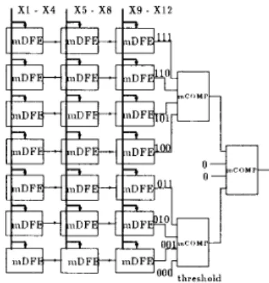
4.3.1. Data-Path Processor: dpp: T h e bit-slice data-path
generation tool, dpp 1401. is perhaps the most important utility f o r algorithm-specific IC's. M u c h of the processing power of such circuits conies from the ability t o dedicate the data-path architecture to the exact needs of the algorithm. With L A G E R the designer can very quickly reconfigure a data path and iterate o n several designs while evaluating their area and performance. Given the schematic of a bit-slice data path, d p p doe5 the place- ment. channel definition, and global routing of the data path
456 IEEE TRANSACTIONS ON COMPUTER-AIDED DESIGN, VOL 10, NO 4, APRIL 1991 Vied Macmcelb (TimLager) Control, SIaIus and Clocks
power rail (mefal2)
Vertical routing channel
I
-c-I
r--J
L A A C A N " E I T nI around rail (melala)
I
HoNontal routing channels
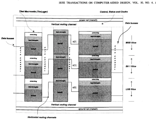
Fig. 10. Bit-slice data path by dpp. Each cell in the block consists of a
leafcell (dark), a feedrhrough (grey) and an optional stretching (white). Horizontal channels are used to route data signals between blocks. Global and local channels are used to route control, status, and clock signals. Each block is generated by TimLager. Routing of blocks is done by Flint.
and produces a floorplan (a FDL file) for Flint to route the in- dividual channels and generate the actual layout. It also back- annotates the structure-instance view of individual macrocells in the data path with geometric constraints and feedthrough in- formation for TimLager.
Bit-sliced data paths (Fig. 10) are viewed by dpp to consist of macrocells that are tiled in the vertical direction and placed linearly along the horizontal direction with the bottom edges of the macrocells being co-linear. Horizontal routing channels separate adjacent macrocells. Local vertical channels are placed along the top edge of each macrocell in order to equalize the heights of each macrocell. Finally, global vertical channels spanning the entire width of the data path are placed at the top and the bottom of the data path.
The control, status, clock, and supply nets run vertically. Within a macrocell they are routed implicitly by the abutment of leafcell terminals during the tiling process. The global rout- ing of these nets between macrocells and to the outside is done by dpp using the global vertical channels. The data buses flow in the horizontal direction and are routed explicitly using the horizontal routing channels between the adjacent macrocells. Data buses connecting nonadjacent macrocells are routed
through the intervening macrocells. This is done by back-an- notation of the structure-instance view of the macrocells with information for TimLager to generate enough feedthroughs for data buses going across the macrocell. Feedthroughs already provided by the leafcell designer are used first before extra feedthroughs are generated.
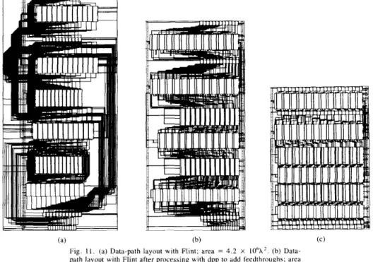
The process of guiding the lower level layout generation ac- cording to the requirements of the upper level layout generator is a key feature of dpp. It makes the macrocells appear porous
Data busses
/
I
I
MS8 Slice4
1
Bit 1 SliceT
I
LS8 Sliceto Flint and saves the area wasted by the macrocell place-and- route approach in routing around the opaque macrocells. As shown by the example in Fig. l l ( a ) and (b), this results in a 24% reduction in area. A problem with our approach is that there may be a mismatch between the heights of adjacent ma- crocells resulting in a staircase effect or congestion in the hor- izontal routing channels. Back-annotation is again used here to force TimLager to stretch the heights of the leafcells used in each bit position in all the macrocells to a uniform value. This equalizes the macrocell heights resulting in much better routing channels. A further 32% reduction in area is obtained in the same example (Fig. 4.7(c)). It can be shown that the percent area penalty due to the staircase and the macrocell opacity effect increases with the number of bits. Consequently, the percent area reduction obtained by making the macrocells porous and stretchable also increases as the number of bits increases. For example, a 24-b version of the same data path shows a 63% reduction in area.
The other crucial step in dpp is placement. The goal is to find a suitable ordering of the macrocells so as to minimize the area. With our approach of through-the-macrocell routing of global buses and equalization of the macrocell heights, the problem can be quite accurately modeled as minimization of the height of the tallest macrocell taking the extra feedthroughs required into account. Dpp directly calls TimLager in an estimation mode to obtain informqtion about the physical characteristics of the macrocells. This information is then used by the placement pro- cedure which is based on the Kemighan and Lin's min-cut placement algorithm [41], but tries to minimize the height of
the tallest macrocell taking the extra feedthroughs required into account, instead of the number of nets crossing a partition.
SHUNG ef al.: CAD SYSTEM FOR IC DESIGN 451
Fig. 11. (a) Data-path layout with Flint; area = 4 . 2 x IO‘X’. (b) Data- path layout with Flint after processing with dpp to add feedthroughs; area = 3 X 10%’. (c) Data-path layout with Flint after processing with dpp to
add feedthroughs and stretching of cells; area = 2.18 x 10‘X’.
4.3.2. Logic Synthesis: Bds2stdcell: The logic synthesis
tools BDSYN [42] and mis-I1 [43] are used by Bds2stdcell to translate a combinational logic description for a module in the BDS language to a logic schematic using a standard cell library. The standard cell layout can then be generated using Stdcell. Bds2stdcell reads the logic description and external terminal in- formation from the structure-instance view of the logic module. After executing BDSYN and mis-I1 it back-annotates the struc- ture-instance view with the actual schematic (nets and sub- cells). Thus the designer can define the logic module as part of the input architecture description and connect it to other mod- ules in the chip without having to provide the detailed sche- matic.
4.3.3. PLA Optimization: Plagen: The plagen structure-
processor reads the BDS logic description for a PLA from the structure-instance view and back-annotates it with the input- plane and output-plane bit patterns for the PLA. After being minimized by espresso [44], the PLA layout can then be gen- erated by a PLA generator using TimLager.
In summary, we see that structure-processor tools can be used to back-annotate the structure-instance view with information for the layout generation tools. This back-annotation may con- sist of defining parameter values required by the macrocell gen- eration (as in plagen and dpp) or defining the schematic itself (as in bds2stdcell). This allows the designer to exploit high- level tools on individual cells in the architecture while retaining a common input structural description.
V . DESIGN EXAMPLES
Application-specific IC’s for a variety of applications have been designing using the LAGER system. They include a low- level trajectory controller for a two-joint robot arm 1451, a chip set for real-time emulation of communication channels in com-
puter networks [46], a chip set for continuous speech recogni- tion using hidden Markov models [47], [48], a real-time image segmentation chip [49], and an image processing chip for Ra-
don transformation [50], etc. Still under development are chips for digital mobile radio, machine vision, and robotics.
Some of the above chips use only the silicon assembler por- tion of the LAGER system. These chips use hardwired archi- tectures because programmable architectures are not suitable due to either higher computation requirements, as in image pro- cessing applications, or specialized U0 requirements, as in the chips for the network channel emulator. Use of a hardwired architecture precludes the use of the behavioral mapper. How- ever, the design of these chips is facilitated by the silicon as- sembler, which enables fast, automatic generation of layout from a netlist description.
Other chips, such as the robot arm controller, the adaptive equalizer for digital mobile radio, and the inverse kinematics processor for a six-joint robot arm, use algorithms that are bet- ter suited to the programmable architectures such as the Kappa model. They have been designed or are being designed using both the behavioral mapper and the silicon assembler.
Section V-5.1 describes a robot arm controller chip, which was designed using both the behavioral mapper and the silicon assembler. Section V-5.2 describes a chip for real-time image segmentation, which was designed with the silicon assembler. In Section V-5.3 we present the design results of several other algorithm-specific IC’s in hardwired architectures.
5.1. Robot Arm Controller Chip
The robot arm controller chip [45] is the heart of a robot- control system that directs a two-joint, direct-drive robot arm along a desired trajectory in real time. It uses a model-reference
458 IEEE TRANSACTIONS ON COMPUTER-AIDED DESIGN, VOL. 10, NO. 4, APRIL 1991
EXTERNAL TESTMOOE
CONDITIONS RESET EOB SCANOUT CLOCKIN TEST CLOCK
I
I
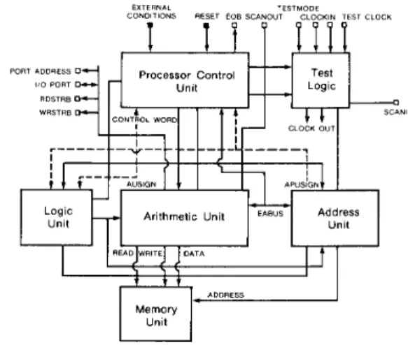
UnitFig. 12. Processor architecture of a Kappa example used in the robot arm controller chip. The solid lines from the processor control unit (PCU) are the control signals. The dotted lines from the data paths are the status sig- nals.
I
proc-chip.sdlI
I I
Fig. 13. The structural hierarchy of the robot arm controller chip. The six blocks at the bottom correspond to the six components in Fig. 12.
the nonlinearities in the arm dynamics and adaptively deter- mines the parameters of the arm at runtime.
On an IBM PC, the MRAC algorithm achieves a 7-ms sample period. Implemented on a TMS32010-based board, it achieves a sample period of 0.7 ms, but at a significant cost in hardware and board area. For a higher speed, a more complex algorithm, or a reduced amount of hardware, a custom chip is appropriate. The custom robot arm controller chip not only achieves a higher speed with a sample period of 0.04 ms, but also reduces the required I/O hardware by customizing the chip I/O.
The chip was designed using the Kappa model architecture. The robot-control algorithm, unlike many DSP algorithms, has many conditional branches and loops. The Kappa control unit provides hardware for efficient handling of these operations. The chip consists of the following functional units, as shown in Fig.
12.
Processor Control Unit: This controls program execution and provides support for branching, looping, and subroutines. It consists of a finite state machine and a control store.
Arithmetic Unit: This is the main data path, used to perform fixed-point arithmetic. It consists of a bit-slice data path and a block of random logic for decoding control signals.
Logic Unit: This is a finite state machine implementing
Boolean operations.
Address Processing Unit: This is an auxiliary data path that performs address computations. Like the arithmetic unit, it con- sists of a bit-slice data path and a block of random logic for decoding control signals.
Memory Unit: This is a random-access, read-write memory, closely tied to the arithmetic unit.
Testing Module: This is an interface for an external tester. It supports testing and debugging of the chip using the scanpath technique.
The layout of the chip is generated from a parameterized structural description. The chip is described hierarchically, using SDL files as shown in Fig. 13. The components are gen- erated using the tools best suited to their layout style; an appro- priate layout generation tool is associated with each SDL file.
At the top-most level of the hierarchy, the chip consists of four pad groups (one for each side) and a core section. The five units are connected by Padroute. The pad groups are assembled as linear tilings of pads using TimLager. The core section con- sisting of the six functional units described above is generated using Flint. The finite state machine PLA’s, the control store,