Robust Reference Clock Generator Design for DDR Synchronous Devices
10
0
0
全文
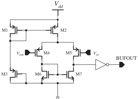
(2) the mentioned problems [1]. Then, a modified. low level.. Then, the output of CED,. NAND circuit with a delay-adjustable feedback. BUFOUT, is pulled high.. is presented to generate a phase-clocked pulse train. The proposed design is verified by using. 2). When VIN < VINB, the output node of the. CADENCE and HSPICE, and the process to. differential amplifier is pulled up to a high. carry out the entire design is TSMC 1P4M 0.35. level. Then, the output of CED, BUFOUT,. µm CMOS technology.. is pulled low.. 2. Clock Generator Circuitry. 3). Since the differential amplifier possesses a high rejection ratio to the common noise. To increase the data throughput, the. which are introduced either by process. transmission scheme has been promoted from. variations or supply noise, the noise. SDR (single data rate) to DDR. This feature. immunity is highly improved.. demands that two correctly out-of-phase pulses are generated given a single clock. The. 4). The reason why the PMOS pair is used. to. instead of a NMOS pair is that the PMOS. synchronize internal pipelines, or output data. pair can be placed inside a single N-well,. buffers. The proposed design is partitioned into. which that the noise coupled from the. two parts, clock edge detection circuit and pulse. substrate is isolated.. generated. clock. pulses. can. be. used. generator circuit as shown in Fig. 2, to resolve such a problem.. 2.1. Clock edge detection circuit. 2.2. Pulse generator The pulse generator, as shown in Fig. 4, is responding to the output of the CED to generate. Owing to the inverter in Fig. 1 will. an internal clock.. The pulse generator consists. unavoidably introduce a delay in the pulse clock. of a NAND- based responding circuit composed. corresponding to the falling edge of the given. of M8 through M11, a keeper composed of M12. clock. We propose another design in Fig. 3,. and inverter INV4, an output inverter in INV5,. where the CLK and CLKB are simultaneously. and a feedback delay circuit in INV2 and INV3.. fed into two clock edge detection (CED) cir-. The detailed operations are described as follows.. cuitry followed by their corresponding pulse generators. The CED is composed of a PMOS. 1). When the input signal at PIN is low, M8. pair differential amplifier as shown in Fig. 3[1].. and the keeper respond and keep the node. The operation of the CED is summarized as. PRES at a high voltage. In the mean time,. follows.. the output, POUT, turns low. In the steady state, M9 is off and M11 is on.. 1). When VIN > VINB, the output node of the differential amplifier is pulled down to a. 2). As soon as PIN turns high, M10 is turned.
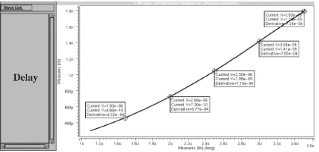
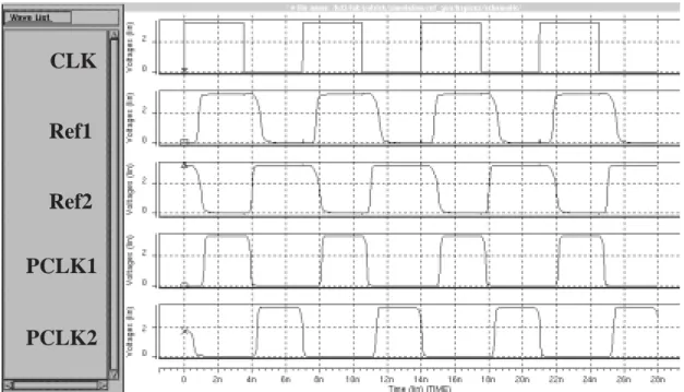
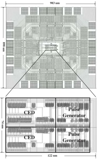
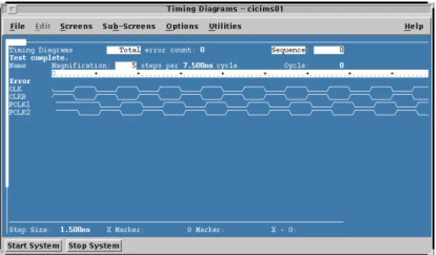
(3) on while M11 is initially on. Hence, PRES. reject the glitch of which the magnitude is over. is pulled to ground through M10 and M11. 1/2 VDD.. which in turn pull POUT to VDD level.. Noise Rejection : Fig. 7 shows another scenario that the external clock is contaminated with high. 3). The low voltage at PRES will be. frequency noises.. Again, the noises are filtered. propagated through INV3 and INV2 to cut. before the internal clocks.. off M11 and turn on M9.. Hence, the. Power Failure Sensitivity : Since the power. voltage at PRES will be back to a high. supply voltage will likely be dropped owing to. level.. aging problems or defective batteries. The voltage drop of the supplied will drastically. 4). The positive pulse width, therefore, is. affect the performance of the clocks.. Fig. 8. determined by the delay of the feedback. shows an impressive result when the supply. network, i.e., INV2 and INV3.. voltage is reduced by 10%. The sensitivity of the edge jitter is 0.62 ns/V.. The pulse width is predicted to be proportional to the delay of INV2 and INV3.. 3.2. Chip characteristics. Fig. 5 is a simulated result using TSMC 0.35 µm 1P4M CMOS process to verify this prediction.. A prototype chip (or IP, i.e., intellectual. The width of the PMOSs in INV2 and INV3 is. property) is shown in Fig. 9. The physical. set to 4.0 µm, while that of NMOSs is set to 2.0. implementation of the proposed clock generator. µm. Referring to Fig. 5, the pulse width vs. the. has been approved to be fabricated on silicon by. lengths of the MOSs are almost linear. This. TSMC and CIC given the number : S35-. result relaxes the complexity of determining the. 90A-15u. Table 1 summarizes the characteristics. duty cycle when given a clock frequency.. of the chip.. 3. Simulations and Measurement By using TSMC (Taiwan Semiconductor Manufacturing. Company). 0.35. µm. 1P4M. Table 1 : The characteristics of the chip die area (with pads). 983×898µm2. core area (without pads). 122×74µm2. max. freq.. 178 MHz. CMOS process, we realize the proposed design. power dissipation @ 133 MHz. 13.3 mW. to meet the DDR requirement of PC-133. power dissipation @ 178 MHz. 15.3 mW. mainboards.. transistor count. 3.1. Post-layout simulations. 44. Referring to Fig. 10, the die photo of the proposed design is proved on silicon. Fig. 11 is. Glitch Rejection : Fig. 6 shows a common. the measured waveforms given a 133-MHz. scenario that the external clock is coupled with a. external clock, while Fig. 12 is the waveforms. periodical glitch noise. The proposed design can. when the Vdd is dropped by 10%. They are.
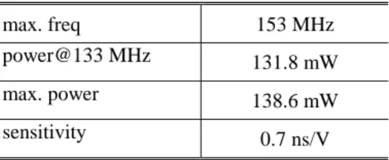
(4) adequate to show the functional correctness of the chip. Table 2 is the measurement of the. [3]. T. Takimoto, N. Fukunaga, M. Kubo, and N. Okabayshi, “High speed SI-OEIC. physical chip by the IMS-200 tester.. (OPIC) for optical pickup,” IEEE Trans. on Consumer Electronics, vol. 44, no. 1,. Table 2 : Measurements of the chip max. freq power@133 MHz. 131.8 mW. max. power. 138.6 mW. pp. 137-142, Feb. 1998.. 153 MHz. sensitivity. [4]. A. Terukina, T. Nozawa, Y. Suzuki, A. Hino, S. Koyama, and A. Moritani, “A. 0.7 ns/V. high precision (+/- 100 ppm) CMOS clock generator),” IEEE 1993 Custom Integrated Circuits Conference, pp. 27.3.1 - 27.3.4,. 4. Conclusion. 1993. A simple and noise-insensitive design for internal clock generation is presented.. It is. [5]. C.-Y. Yang, G.-K. Dehng, J.-M. Hsu, and. highly suitable for DDR applications. It can be. S.-I. Liu, “New dynamic flip-flops for. either implemented in a single chip or in an IP. high-speed dual-modulus prescaler,” IEEE.. (intellectual property) form to be included in a. J. of Solid-State Circuits, vol. 33, no. 10,. system chip.. pp. 1568-1571, Oct. 1998.. Reference. [6]. T. Yoshimura, H. Kondoh, Y. Matsuda, and T.. [1]. [2]. Sumi,. “A. 622-Mb/s. bit/frame. P. R. Gray, and R. G. Meyer, “Analysis and. synchronizer for high-speed backplane. design of analog integrated circuits,”. data. Reading: 3rd edition, John Wiley & Sons,. Solid-State Circuits, vol. 31, no. 7, pp.. Inc., 1993.. 1063-1066, July 1996.. P. Larsson, and C. Svensson, “Impact of. [7]. communication,”. IEEE.. J.. of. C.-C. Wang, Y.-T. Chien, and Y.-P. Chen,. clock slope on true single phase clocked. “A practical load-optimized VCO design. (TSPC) CMOS circuits,” IEEE. J. of. for. Solid-State Circuits, vol. 29, no. 6, pp.. phase-locked loop,” VLSI Design, vol. 11,. 723-726, June 1994.. no. 2, pp. 107-113, June 2000.. low-jitter. 5V. 500. MHz. digital.
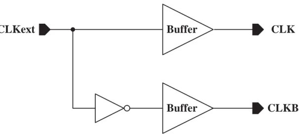
(5) CLKext. Buffer. CLK. Buffer. CLKB. Figure 1: Traditional out-of-phase clock generator. CLK CED. Pulse Generator. PCLK1. Pulse Generator. PCLK2. Ref1. CLKB. CED Ref2. Figure 2: Block diagram of the proposed DDR clock generator.
(6) Vdd. M1. M2. M4. VINB. M3. M5. M6. VIN. BUFOUT. M7. Figure 3: Schematic view of the clock edge detector (CED). Vdd INV4 M8. PIN (BUFOUT). M9. M12. INV5. POUT (PCLK). Keeper. M10. PRES M11. INV2. INV3. Responding Circuit. Feedback Delay Circuit Figure 4: Schematic view of the NAND-based pulse train generator.
(7) Delay. Figure 5: Diagram of delay vs. length of MOSs in the feedback inverters. CLK Ref1 Ref2 PCLK1 PCLK2. Figure 6: Post-layout simulation waveforms of rejecting glitches (3.3V VDD, 133 MHz external clock).
(8) CLK Ref1 Ref2 PCLK1 PCLK2. Figure 7: Post-layout simulaion waveforms of rejecting noise (3.3V VDD, 133 MHz external clock). CLK Ref1 Ref2 PCLK1 PCLK2. Figure 8: Post-layout simulation waveforms of tolerating 10% VDD drop.
(9) 983 um. 898 um. Pulse Generator. CED. Pulse Generator. 74 um. CED. 122 um. Figure 9: Chip Layout. 74 um. 122 um. Figure 10: Die photo.
(10) Figure 11: Measured waveforms given a 133 MHz clock. Figure 12: Measured waveform when Vdd drops 10%.
(11)
數據
+4
相關文件
In Paper I, we presented a comprehensive analysis that took into account the extended source surface brightness distribution, interacting galaxy lenses, and the presence of dust
[r]
➢The input code determines the generator output. ➢Understand the meaning of each dimension to control
In each figure, the input images, initial depth maps, trajectory-based edge profiles that faithfully enhance bound- aries, our depth maps obtained with robust regression, final
The schematic diagram of the Cassegrain optics is shown in Fig. The Cassegrain optics consists of a primary and a secondary mirror, which avoids the generation of
【Figure 4-50】 The difference of electrical capacity characteristics of specimens at 5 minutes deposition time with various dispersing percentage carbon
The major testing circuit is for RF transceiver basic testing items, especially for LNA Noise Figure and LTE EVM test method implement on ATE.. The ATE testing is different from
This research focuses on the analysis of the characteristics of the Supreme Court verdicts on project schedule disputes in order to pinpoint the main reason for delay
