This content has been downloaded from IOPscience. Please scroll down to see the full text.
Download details:
IP Address: 140.113.38.11
This content was downloaded on 28/04/2014 at 08:28
Please note that terms and conditions apply.
Thin-Film Transistors with Polycrystalline Silicon Films Prepared by Two-Step Rapid Thermal
Annealing
View the table of contents for this issue, or go to the journal homepage for more 2000 Jpn. J. Appl. Phys. 39 L19
(http://iopscience.iop.org/1347-4065/39/1A/L19)
Jpn. J. Appl. Phys. Vol. 39 (2000) pp.L19–L21 Part 2, No. 1A/B, 15 January 2000
c
°2000 Publication Board, Japanese Journal of Applied Physics
Thin-Film Transistors with Polycrystalline Silicon Films
Prepared by Two-Step Rapid Thermal Annealing
Huang-Chung CHENG∗, Chun-Yao HUANG, Fang-Shing WANG, Kuen-Hsien LINand Fu-Gow TARNTAIR Department of Electronics Engineering and Institute of Electronics, Semiconductor Research Center, National Chiao-Tung University, 1001 Ta Hsueh Road, HsinChu 300, Taiwan, R.O.C.
(Received August 27, 1999; accepted for publication November 1, 1999)
A novel two-step rapid thermal annealing (RTA) process has been developed to significantly reduce the crystallization time for the solid-phase crystallization (SPC) of amorphous silicon films. In comparison with the conventional SPC processes, it not only keeps a low thermal budget but also achieves a larger poly-Si film grain size than that obtained by one-step RTA, and even as large as that obtained by conventional furnace annealing (CFA). Furthermore, poly-Si thin-film transistors fabricated by such a novel annealing scheme possess electrical characteristics superior to those obtained by one-step RTA and comparable to those obtained by long-time CFA.
KEYWORDS: SPC, RTA, CFA, poly-Si TFTs, two-Step RTA
∗E-mail address: [email protected]
L19
1. Introduction
In the last decade, polycrystalline silicon thin-film transis-tors (poly-Si TFTs) have received much attention, in particu-lar, for active-matrix liquid crystal displays (AMLCDs) with on-glass peripheral circuits and 3-D integrated circuits.1–3) Unlike the transistors fabricated on bulk silicon substrates, the performance of poly-Si TFTs is strongly influenced by the grain boundaries and intragranular defects. In order to im-prove the performance of poly-Si TFTs, the recrystallization of silicon films4–8) has been widely investigated to enlarge the grain size and reduce the defect-state density in poly-Si films. In addition, AMLCDs, fabricated on glass substrates, require a low-thermal-budget process to avoid any degrada-tion of glass substrates. However, the conventional low-temperature (600◦C) furnace annealing in solid phase crys-tallization (SPC),consisting of incubation and cryscrys-tallization steps, usually requires more than 10 h for full crystallization. The use of rapid thermal annealing (RTA)9–12) enables effi-cient reduction of the thermal budget and cycle time of the processes, which results in a substantially higher throughput than with conventional furnance annealing (CFA). Neverthe-less, the grain size of a poly-Si film annealed by RTA is much smaller than that obtained by CFA. Recently, new annealing methods which combine CFA and RTA13, 14) have been pro-posed to obtain high-quality poly-Si films and to reduce the annealing time for crystallization of a-Si films. On the other hand, it still takes a few hours to achieve full recrystalliztion. In this work, a novel two-step RTA method is proposed for the recrystallization of a-Si films. By this way, it not only re-duces the annealing time from several hours to a few minutes but also enables the realization of high-quality poly-Si films of grain size as large as that in the case of long-time CFA. The electrical characteristics of poly-Si TFTs fabricated by various annealing methods are also compared and discussed.
2. Experimental Procedures
The poly-Si films were fabricated on thermally oxidized silicon wafers. A 100-nm-thick a-Si film was initially de-posited at 475◦C by low-pressure chemical vapor deposition (LPCVD) using Si2H6gas. The crystallization was performed by the two-step RTA technique, in which the a-Si films were
at 600◦C for the LT case. After opening the contact holes, the Al films were evaporated and then patterned. For evalua-tion of the simple effects of the different annealing processes on the TFT characteristics, no further hydrogenation was per-foemed. The final TFT had a conventional coplanar structure and the W/L ratio was 50 µm/10 µm.
3. Results and Discussion
Figure 1 shows the plan-view bright-field TEM micrograph of the 100-nm-thick silicon film annealed by (a) one-step RTA (750◦C/120 s), (b) two-step RTA (550◦C/60 s + 750◦C/60 s), and (c) CFA (600◦C/20 h). As can be seen in Fig. 1(a), the grains in the case of the one-step RTA process exhibit a den-dritic structure and the grain size, as estimated by dark-field TEM, is around 0.8µm. The structure of the silicon films an-nealed by two-step RTA, as shown in Fig. 1(b), is similarly dendritic and the grain size is about 1.5µm. The result is al-most similar to that for an a-Si film annealed by long-time CFA, as shown in Fig. 1(c). It is noteworthy that the CFA takes 20 h to crystallize the a-Si film, while the two-step RTA takes only 2 min. Therefore, the crystallization time of SPC can be significantly reduced with no associated reduction in grain size by applying the new annealing scheme.
To verify the electrical properties of the poly-Si films first annealed at 550◦C for 60 s and then at 750◦C for 60 s. In addition, comparison for films were also annealed by either CFA at 600◦C for 20 h or one-step RTA at 750◦C for 120 s. The structure and the grain size of the crystallized poly-Si films were determined by transmission electron microscopy (TEM). In order to evaluate the electrical characteristics of the poly-Si films, two sets of TFTs were separately fabricated us-ing high- and low-temperature processes, denoted as HT and LT. After defining the active islands, 60-nm-thick gate oxide was thermally grown by dry oxidation at 900◦C for the HT process and SiNxwas deposited as gate dielectrics by
plasma-enhanced CVD (PECVD) at 300◦C for the LT process. There-fore, another 250-nm-thick a-Si film was deposited at 560◦C in a LPCVD system using SiH4and patterned as the gate elec-trodes. Self-aligned phosphorus ion implantation with energy of 50 keV and dose of 5E15 cm−2was used to dope the drain, source, and the gate areas. Prior to the dopant activation, a 500-nm-thick encapsulation oxide was deposited in a PECVD system. The implanted dopants were activated by 40-min an-nealing at 850◦C for the HT samples and by 12-h annealing
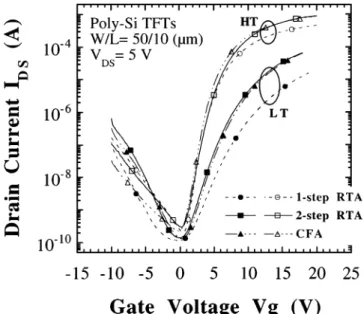
formed by the new annealing technique, n-channel poly-Si TFTs were fabricated and the current–voltage (I –V ) charac-teristics of the TFTs were measured by an HP 4156A pre-cise semiconductor parameter analyzer. Figure 2 gives the typical Id–Vg transfer characteristics for the differently pro-cessed TFTs at VDS = 5 V. The extracted electrical pa-rameters from the plot, including the threshold voltage, the on/off current ratio, the field effect mobility, the subthresh-old swing, and the trap-state density, are all listed in Table I. The trap-state density Nt is obtained by using the theory es-Fig. 1. Plan-view bright-field TEM micrographs of 100-nm-thick silicon films crystallized by (a) one-step RTA (750◦C/120 s), (b) two-step RTA (550◦C/60 s + 750◦C/60 s), and (c) CFA (600◦C/20 h).
Fig. 2. The Id–Vg transfer characteristics of n-channel poly-Si TFTs at
VDS = 5 V, fabricated using HT and LT processes with various
crystal-lization methods. The W/L is 50 µm/10 µm.
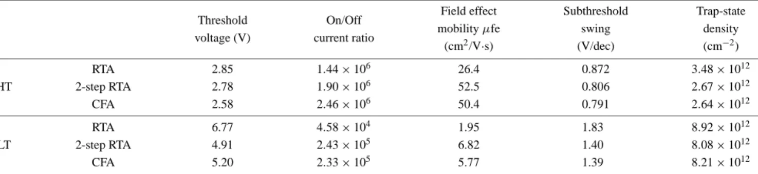
tablished by Levison et al.15) and Proano et al.16) Whether the HT or LT process is used, it is evident that the two-step RTA specimens exhibit superior electrical performance such as higher field-effect mobility, on/off current ratio, lower threshold voltage, and trap-state density. The enhancement of the TFT characteristics is attributed to the larger grain size and lower trap-state density achieved by the two-step RTA method. As to the enlarged grain size obtained by two-step RTA, the first low-temperature RTA (550◦C/60 s) is thought to play an important role during crystallization. It is presumed that the first low-temperature RTA induces the formation of a few nucleation sites which then enlarge during the second high-temperature RTA (750◦C/60 s). In contrast, one-step RTA at 750◦C induces the rapid formation of a mass of nu-cleation sites everywhere, which results in a small grain size. Further compared with CFA-TFTs, the devices fabricated by the two-step RTA possess similar electrical characteristics to those of the TFTs fabricated by CFA. The similar electri-cal performances of the TFTs fabricated by these two meth-ods are believed to be due to their similar microstructures and grain size. The lower field effect mobility, as compared with that of films fabricated by Excimer laser annealing (ELA), can be attributed to the crystallinity of the poly-Si films. The poly-Si film subjected to solid-phase crystallization of RTA and CFA has more defects than that in case of liquid-phase crystallization by ELA. These defects include intra-grain de-fects and high-angle grain-boundaries within the active chan-nel portion of the TFTs. Hence, the field effect mobility of the poly-Si TFTs fabricated by CFA or two-step RTA is relatively lower than that of the TFTs fabricated by ELA.
4. Summary and Conclusions
In conclusion, a new annealing method, two-step RTA, was developed to obtain high-quality poly-Si films. The grain size of poly-Si films obtained by this two-step RTA is twofold that in the case of one-step RTA and as large as that obtained by CFA. Poly-Si TFTs with an active layer prepared by this novel method have superior electrical characteristics to those
fabricated by one-step RTA, comparable to those obtained by CFA. Since the two-step RTA can significantly improve the characteristics of the poly-Si TFTs at a lower thermal budget and manufacturing cost, its use is recommended for applica-tion to poly-Si TFT/LCDs.
Acknowledgments
This research was supported in part by the Republic of China (ROC) National Science Council under Contract No. NSC-89-2215-E009-069. The technical support from the Semiconductor Research Center in National Chiao Tung Uni-versity and the National Nano Device Laboratory is also ac-knowledged.
1) S. Morozumi, K. Oguchi, S. Yazawa, T. Kodaira, H. Ohshima and T. Mano: SID’83 Dig. (1983) p. 156.
2) A. Mimura, N. Konishi, K Ono, J. Ohwada, Y. Hosokawa, Y. Ono, T. Suzuki, K. Miyata and H. Kawakami: IEEE Trans. Electron Devices 36 (1989) 351.
3) M. Kinugawa, M. Kakamu, T. Yoshida, T. Nakayama, S. Morita, K. Kubota, F. Matsuoka, H. Oyamatsu, K. Ochii and K. Maequchi: VLSI
Technol. Dig. Tech. Papers (1990) p. 23.
4) M. K. Hatalis and D. W. Greve: IEEE Electron Device Lett. 8 (1987) 361.
5) R. B. Iverson and R. Reif: J. Appl. Phys. 62 (1987) 1675. 6) Y. Moria and T. Noguchi: Jpn. J. Appl. Phys. 28 (1989) L309. 7) K. Sera, F. Okumura, H. Uchida, S. Itoh, S. Kaneko and K. Hotta: IEEE
Trans. Electron Devices 36 (1989) 2868.
8) T. Aoyama, G. Kawachi, N. Konishi, T. Suzuki, Y. Okajima and M. Miyata: J. Electrochem. Soc. 136 (1989) 1169.
9) R. Kakkad, J. Smith, W. S. Lau and S. J. Fonash: J. Appl. Phys. 65 (1989) 2069.
10) M. Bonnel, N. Duhamel, M. Guendouz, L. Haji, B. Loisel and P. Ruault: Jpn. J. Appl. Phys. 30 (1991) L1924.
11) M. Bonnel, N. Duhamel, T. Henrion, B. Loisel and L. Haji: J. Elec-trochem. Soc. 140 (1993) 3584.
12) L. Hajj, P. Joubert, J. Stoemenos and N. A. Economou: J. Appl. Phys. 75 (1994) 3944.
13) M. Bonnel, N. Duhamel, L. Hajj, B. Loisel and J. Stoemenos: IEEE Electron Device Lett. 14 (1993) 551.
14) K. S. Nam, Y. H. Song, J. T. Baek, H. J. Kong and S. S. Lee: Jpn. J. Appl. Phys. 32 (1993) 1908.
15) J. Levison, F. R. Shepherd, P. J. Scanlon, W. D. Westwood, G. Este and M. Rider: J. Appl. Phys. 53 (1982) 1193.
16) R. E. Proano, R. S. Misage and D. G. Ast: IEEE Trans. Electron Devices 36 (1989) 1915.
Jpn. J. Appl. Phys. Vol. 39 (2000) Pt. 2, No. 1A/B H.-C. CHENGet al. L21
Table I. The values of the threshold voltage, the on/off current ratio, the field effect mobility, the subthreshold swing and the trap-state density of poly-Si TFTs fabricated using HT and LT processes with various SPC techniques. The threshold voltage is defined at a fixed drain current Id= Idn×W/L, where Idnis the normalized drain current, 10 nA. The subthreshold swing and field effect mobility
were measured at VDS = 0.1 V for W/L = 50 µm/10 µm. The on/off current ratio is the drain current measured at VDS= 5 V and
VG= 15 V over the minimum value of the drain current measured at VDS= 5 V.
Threshold On/Off Field effect Subthreshold Trap-state voltage (V) current ratio mobilityµfe swing density
(cm2/V·s) (V/dec) (cm−2) RTA 2.85 1.44 × 10⁶ 26.4 0.872 3.48 × 10¹² HT 2-step RTA 2.78 1.90 × 10⁶ 52.5 0.806 2.67 × 10¹² CFA 2.58 2.46 × 10⁶ 50.4 0.791 2.64 × 10¹² RTA 6.77 4.58 × 10⁴ 1.95 1.83 8.92 × 10¹² LT 2-step RTA 4.91 2.43 × 10⁵ 6.82 1.40 8.08 × 10¹² CFA 5.20 2.33 × 10⁵ 5.77 1.39 8.21 × 10¹²