國
立
交
通
大
學
電信工程研究所
碩
士
論
文
分裂諧振環應用於矩形波導中的參數研究與建立其多項式曲
線擬合
A Parametric Study of SRR loaded Rectangular Waveguides
and Modeling with Polynomial Curve Fitting
研 究 生:包佳琪
(Lallah Badjie)
指導教授:黃謀勤 博士 (Dr. Malcolm Ng Mou Kehn)
分裂諧振環應用於矩形波導中的參數研究與建立其多項式曲線擬合
A Parametric Study of SRR loaded Rectangular Waveguides and Modeling
with Polynomial Curve Fitting
研 究 生:包佳琪
(Lallah Badjie)
指導教授:黃謀勤 博士 (Dr. Malcolm Ng Mou Kehn)
A thesis
Submitted to Institute of Communication Engineering
College of Electrical Engineering and Computer Engineering
National Chiao Tung University
For Obtaining The Degree of Master
In
Communication Engineering
August 2012
I
A Parametric Study of SRR loaded Rectangular Waveguides and Modeling
with Polynomial Curve Fitting
Student: Lallah Badjie Advisor: Dr. Malcolm Ng Mou Kehn Institute of Communication Engineering
National Chiao Tung University
I.
Abstract
Metamaterial though is a new research area in electromagnetic engineering has attracted many investigators recently. The loading of these metamaterial elements have been presented here. My thesis carried out a parametric on rectangular waveguide with SRR metamaterial aim at investigating dimensional and electrical properties on the behavior of the backward wave mode on the dispersion diagrams. By inserting identical SRRs on two side walls of the rectangular waveguide create a pass-band below the waveguide cutoff frequency, thereby supporting backward travelling waves. SRRs are negative permeability media periodic structures loading into rectangular waveguide possess backward wave mode existing within the narrow pass-band below the cutoff frequency. Parameters involved in the design configuration have been investigated and their effects and influences on the appearance and locations of the backward wave mode on dispersion diagrams have been analyzed. A range of parameters that can be used to produce a better design and obtained good results as expected were identify. One major success of this study conducted is a way of computing the CST simulation in the shortest period of time which does not only speed up the work but ease the tension of the work. Optimization of the design parameters has been presented. This method shows the overlapping areas of the parameters involved. Another method called the polynomial curve fitting technique for modeling the estimated data from the dispersion diagrams have been presented too.
II
II. Keywords
Metamaterials, Split ring resonators (SRR), backward wave, Pass-band .
III.
Acknowledgements
First, I would like to thank my advisor Professor Malcolm Ng Mou Kehn for his support on this thesis and the helped with suggestions and comments of some of the results presented in this thesis. Finally, my thoughts go to my family and to my friends for their sensible advises and
III
TABLE OF CONTENTS
I. Abstract………...I
II. Keywords………...II
III. Acknowledgements………II
CHAPTER 1
INTRODUCTION
………1
I. Metamaterials……….1
II. Motivation and objectives………..2
III. Contributions………..2
CHAPTER 2
CONFIGURATION AND METHODOLOGY
I. Introduction………..3
II. Rectangular waveguides TE modes ………3
III. SRR array loaded rectangular waveguide………6
CHAPTER 3
RESULTS AND ANALYSIS
………9
I. Parametric study………..………9
II. CST Simulations………22
III. Map design application………..41
IV
CHAPTER 4
CONCLUSIONS
………60
I. Summary………60
II. Future work………62
III. Reference………62
1
CHAPTER 1
Introduction
This chapter contains about the artificial man-made materials that are not readily occurring in natural materials. These artificial materials called metamaterials are briefly reviewed. The motivation and goals of this thesis work have been discussed. The applications in electromagnetic engineering have been also described. Finally the structure of the thesis is presented.
I. Metamaterials
The termed metamaterial have been a research of interest among the researchers all over the world for a decade now. There are several names associated to metamaterials and its definition nonetheless they are man-made materials that have the ability to exhibit properties that may not occur in nature [1]. The unique properties (negative permeability and permittivity) possess or exhibited by this man made materials are due to the periodic arrangement and their design configurations unlike natural occurring elements that exhibits properties due to the atomic molecules that make them up [2]. There are various types of metamaterial but on this thesis electromagnetic metamaterial will be presented [3-4]. Since the introduction of metamaterial in the early sixties, metamaterial has not only attracted scientist but the insertion of these metamaterial elements into rectangular waveguide has been an intense research recently [5-6]. Previous work of authors has proposed the used of periodically arranged metamaterial elements (SRRs) on different locations within the waveguide but with this different approaches all these authors have a common goal which is the realization of backward wave mode within a narrow pass-band and stop-band below and above waveguide cutoff frequencies respectively[7-11]. SRR loaded waveguide configuration can either possess pass-band or stop-band depending on the SRR resonance frequencies below and above the cutoff frequencies of the waveguide.
Waveguide are guiding structures that allow the propagation or transmission of electromagnetic waves. In a typical waveguide (X-band waveguide) structures without any filling behaves as a high pass filter allowing transmission above the cutoff frequency. The transmission of X-band waveguide occurs at cutoff frequency of 8GHz to 12GHz but when it was filled with a material backward wave exist but the cutoff frequency shift down from 8GHz to 4.5GHz as indicated in figure 1 (b). Figure1.1 shows the X-band waveguide response of both waveguides with or without fillings.
2
Fig. 1.1 X-band waveguides response with or without fillings, (a) waveguides response without fillings, (b) waveguides response with fillings
II. Motivation and objectives
Before the start of this study, I have no idea or little did I know about metamaterial element (SRR) loaded rectangular waveguide but reading papers by different authors I now have a picture of this widely research topic. As mentioned earlier recent authors has conducted an investigation on SRR loaded rectangular and the objective of this research was among obtaining a backward wave mode existing within a narrow pass-band of the cutoff frequency thereby creating an environment for backward wave propagation. But this has not been an easy task due to the challenges encountered in the research process. Though several researchers conducted this study, the challenges encountered motivated me to conduct the same study in order to investigate for a remedy to this problem. The challenges include: the design configuration of SRRs loaded rectangular waveguide which is difficult to draw, the electrical and structural dimensions of the design configuration which have great impact towards the realization of obtaining a pass-band below the cutoff frequency. The CST simulation of the configuration was also a course of concern due to the time consumed during the simulation process. The need to consume less time during the simulation was a necessity to ease the tension of the work.
III. Contributions
To improve the challenges described in the study of SRR loaded rectangular waveguide, a parametric study have been conducted. The parametric study based on the input parameters of the design structure was aim at investigating the influence of different parameters and their effects on the performance of the proposed waveguide. The exhibition of backward wave mode
3
existing within the narrow pass-band below the waveguide cutoff frequency was the main objective of this study. The parametric study performed build on pervious study by other authors [8, 12] were the electrical, structural and dimensional properties of the SRR loaded rectangular waveguide have been investigated observing the behavior of the backward wave. During this parametric study an approach fast enough to perform the CST simulation in the shortest period of time was discovered which forms the most significant contribution of this thesis.
The other aspect of contribution was map design applications and polynomial curve fitting technique. Map designed method have been demonstrated to see the overlapping areas of the SRR loaded waveguide parameters which can be used for engineering applications. The estimated values calculated from the CST dispersion result have been model in polynomial curve fitting technique.
CHAPTER 2
CONFIGURATION AND METHODOLOGY
I. Introduction
This chapter contains a brief review of SRR array loaded rectangular waveguides [7]. The objectives and motivation of this thesis are address on the parametric study. Firstly we review transverse electric TE modes rectangular waveguide however the rectangular waveguide can support both TE and TM modes only the solution of TE mode is provided here and it is also call the dominant mode [13].
II. Rectangular waveguides TE modes
Figure 2.1 is the geometry of rectangular waveguide structure. The coordinate systems are oriented so that the z axis is along the length of waveguide indicating the direction of wave propagation. The horizontal and vertical axes denoted as x and y respectively. a and b denote the width and height respectively. By convention we define a b. and the x axis is oriented along a broader dimension a.
4
Figure 2.1 Rectangular waveguide structures [13]
Taking the wave equation in Cartesian coordinate system which is a scalar equation µє 0
Frequency is ω, permittivity є, and permeability µ respectively. Expanding the in the Cartesian coordinate system to get
µє 0
By using the method of separation of variables to get a solution which is a function of
YZ XZ XY µє XYZ 0
µє 0
The above equation can be reduced into three equations by equating the each term of the above equation to some constants.
5
The three equations above looks like a second order equation which can be written as a forward manner as X(x) Y(y) Z(z) 0 HZ ( )
HZ is a tangential component to four walls of rectangular waveguide as shown in fig… and
boundary conditions are also obtained: x=0, x=a and y=0, y=b. Boundary conditions can be applied to get the arbitrary constants
EZ = 0 at x=0, x=a and y=0, y=b
For x= 0 C1 0
For y =0 C3 0
The general solution that can satisfied the boundary conditions when x=0, y=0 would be
HZ =
Combining the arbitrary constants C5C1C3 to be a C quantity we get
HZ = C
For x= a, EZ = 0 when if Aa are multiples of m , so A =
For y=b, EZ = 0 when if By are multiples of n , so B =
Substitute the value of A and B into the equations. m and n are integers we get the complete solution of the wave equation for the longitudinal components EZ as shown below
C ( ) ( )
Longitudinal components for TE modes Ex =
=
6 Ey = = ( ) C ( ) ( ) Hx = = ( ) C ( ) ( ) Hy = = ( ) C ( ) ( ) Observation of TEmn modes: TE00 does not exist
TEm0 and TE0n modes exist.
TE10 and TE01 is the lowest order of TE mode which existed on the waveguide.
Cutoff frequency c = √ {(
) ( ) }
⁄
From the expression of the cutoff frequency c = √ { (
) ( ) }
⁄
we can substitute for the lowest indices possible in the TE10, TE01
cTE10 = ⁄ √ cTE01 = ⁄ √
Since on the rectangular waveguide we defined a b then
cTE10 cTE01
TE00 do not exist then the lowest frequency that can propagate on this structure is
c TE10 and is the absolute minimum frequency the structure can support and known as
dominant TE10 mode..
III.
SRR array loaded rectangular waveguides
Artificially structured metamaterials waveguides has attracted increasing researchers in recent years, however this study will base on waveguide with SRR metamaterials. Backward travelling waves is one of the unique properties exhibited by SRR loaded waveguides but there are other
7
metamaterial waveguide structures examined by other authors which also have the ability to create an environment for backward wave propagations [14-17]. Regardless of the challenges encountered during the investigation process, great interest has been devoted to waveguide with SRR metamaterials for the past decade. Many investigations have been performed for different SRR parameters and orientation on rectangular waveguide however all created a backward wave mode thereby supporting backward travelling wave. This does not only support electromagnetic wave propagation but also use for waveguide miniaturization [3, 11]. Some focus on other waveguide structures leading to the realization of backward wave mode below the cutoff frequency.
In this thesis SRR loaded rectangular waveguide proposed by [7] have been presented and it was designed to obtain a pass-band below the waveguide cutoff frequency. The identical SRR inserted on two side walls of the rectangular waveguide was reinvestigated again. The design configuration made it possible for the SRR at its resonance frequency below the waveguide cutoff frequency to exhibit a backward travelling wave. This backward wave mode existing within a narrow pass-band below the waveguide cutoff frequency was created by the simultaneously negative permeability and permittivity of the proposed waveguide structure. We reinvestigated SRR loaded rectangular waveguide [7] with width and height of 35mm and 16mm respectively. An SRR inclusion was printed on a conventional fiber glass of relative permittivity of 4.5 with thickness 1.55mm. The SRR dimensions are: outer radius = 7.6mm, inner radius = 6.4mm, gap distance = 1.4mm and unit cell 15.6mm and the geometry of the
proposed waveguide is shown in figure 2.2 The design configuration structure have been computed using CST simulation and the dispersion diagram have been reproduced again as shown in figure 2.3.A backward wave centered at 1.8GHz at a cutoff frequency of 3.9HGz was observed as expected but the variations of SRR has an influence on the location of the backward wave mode. CST software was used for both the dispersion diagram of figure 2.2 and the dispersion diagram of fig. 2. [7], shown as figure 2.4. Comparing the two dispersion diagrams their dispersion results are in agreement, the location of the backward wave modes of the two dispersion diagrams are centered at 1.8 GHz below waveguide the cutoff frequency. With regards to this phenomenon parametric study has been conducted to reinvestigate the factors affecting the location, presence/absence of backward wave mode on the dispersion diagrams. Not only the SRR various size was considered but the parameters of the overall SRR loaded rectangular waveguide structure was looked into. The duration of the CST simulation was also paramount.
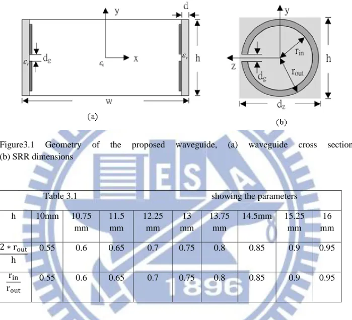
8
Figure 2.2 Geometry of the proposed waveguide, (a) waveguide cross section (b) SRR dimensions
Figure 2.3 Dispersion diagram of the proposed waveguide with SRR of identical sizes on both sides.
9
Figure 2.4.Dispersion diagram of the proposed waveguide with SRR of identical sizes on both sides (solid lines) [7].
CHAPTER 3
RESULTS AND ANALYSIS
I. parametric study
Nowadays recent researchers have design SRR array loaded rectangular waveguide of different orientation on the waveguide structure, however the main concern for these structure design is on how to give suitable range of parameters to meet the design objectives. The existence of a backward wave mode on the dispersion diagram may be due to the inappropriate varying electrical structural and dimensions. Despite several parametric study conducted by other authors
10
they has not been able to show design configuration method which can be computed using CST in the shortest period of time.
The objective of this study is to examine SRR loaded rectangular waveguide configuration to determine the influence and the effects of the input parameters on the existence of backward wave modal pass-band below the cutoff frequency. This parametric study extended from the previous author [8, 12] on Multiband SRR Loaded Rectangular Waveguide. Variation of design input parameters have continue to be a key factor affecting the exhibition of backward wave mode in metamaterial waveguide structures, an impact on the design configuration and also influences the position of the modal pass-band on the dispersion diagrams. This particular parametric study carried out here was able to provide the possibilities of improving the duration of the CST simulations.
A range of parameters are chosen as shown on table 3.1, various designed configurations have been generated and simulated. Each parameter variation and dispersion results have been analyze, thereby demonstrating the variations of the design causing the most effect either good or bad on the dispersion diagram. The different parameters investigated in this study include the following:
Height Width
Relative permittivity Thickness
Outer and inner SRR radii Gap space
The following is a description of the new initial geometry proposed for this parametric study shown in figure 3.1. The gap space in this new geometry is an arc of 𝜙 = equivalent to 0.087rad. Width w = 35mm, = 4.5, thickness d = 1.55mm. Other dimensions are as follows:
Height: height 16mm
SRR radii: and 0.55 0.95 Gap space: 0.55 0.087rad 0.087rad
11
Figure3.1 Geometry of the proposed waveguide, (a) waveguide cross section (b) SRR dimensions
Table 3.1 showing the parameters h 10mm 10.75 mm 11.5 mm 12.25 mm 13 mm 13.75 mm 14.5mm 15.25 mm 16 mm 0.55 0.6 0.65 0.7 0.75 0.8 0.85 0.9 0.95 0.55 0.6 0.65 0.7 0.75 0.8 0.85 0.9 0.95
There were a total number of 729 computed results which all exhibited backward wave on their dispersion diagrams as expected and their respective cutoff frequencies have been observed. Each of the nine different heights as indicated in table 3.1 have 81 total dispersion diagrams. It was also noticed that backward travelling wave made a shift to left as the scaling factors increase in size. The bandwidths and the center frequencies vary due to the effects of the starting and ending points of the backward travelling wave. It can now be conclude that no matter how small the height of waveguide would be, if you keep on increasing the size of SRR with different scaling factors in ascending order backward wave will be observed as expected.
The effects of the waveguide height dimensions ranging from 14.5mm to 16mm and the SRR size variations have been presented here as follows waveguide heights: height 16mm, SRR radii: and 0.55 0.95 , Gap space:
12
0.55 0.087rad 0.087rad. Backward waves mode exist on all the
dispersion graphs of heights 14.5mm, 15.25mm and 16mm but shifting to right as the height increases. There is an influence on the cutoff frequency location. Increasing the heights and the SRR size caused both the backward waves and cutoff frequencies locations on the dispersion graphs to decrease in values and make a shift to the left side due to the constant increase of inner radius whilst maintaining the outer radius of the SRR. Hence the heights and the SRR size variations affect the locations of the backward waves. Below are some of the computed dispersion diagrams and their various bandwidths, center frequencies and cutoff frequencies.
Table 3.2 Height = 14.5mm figures Legend Center
frequencies (GHz) Cutoff frequencies (GHz) Bandwidth (GHz) 3.2 3.42965 7.5 0.047 3.72455 7.64 0.041 4.0931 7.63 0.026 3.10 1.93725 5.58 0.016 2.15255 5.96 0.017 2.38785 6.2 0.01
13
Figure3.2. Height and SRRs dimension effects on dispersion diagrams showing only outer radius of 3.98mm.
The height of the waveguide is 14.5 mm and its width is 35 mm. The relative permittivity of each of the two dielectric side slabs is 4.5 with thickness 1.55mm.3.98 6.88, 0.55
, 0.55 0.087rad 0.087rad, represented in the figure in solid
14
Figure3.3 SRRs dimensions and Height effects on dispersion diagrams showing only outer radius of 3.98mm.
The height of the waveguide is 14.5 mm and its width is 35 mm. The relative permittivity of each of the two dielectric side slabs is 4.5 with thickness 1.55mm.3.98 6.88, 0.55
, 0.55 0.087rad 0.087rad, represented in the figure in solid
lines, asterisk lines and point lines respectively.
Looking at the above graphs with the same height of 14.5mm, it have been noticed that both the backward wave modes and the cutoff frequency values all shift to the right side as their outer and inner diameters of the SRRs increases. Both the outer and inner diameters of the SRRs rings have be scale by factors [0.55 0.6 0.65 0.7 0.75 0.8 0.85 0.9 0.95]. The higher the scale factor backward wave modes and their respective cutoff frequencies shift to the left side.
Table3.3 Height = 15.25mm figures Legend Center
frequencies (GHz) Cutoff frequencies (GHz) Bandwidth (GHz)
15 3.11 2.97465 7.38 0.0407 3.5252 7.6 0.0396 3.88745 7.6 0.0251 3.19 1.84425 5.345 0.0155 2.05645 5.76 0.0151 2.2714 5.99 0.0092
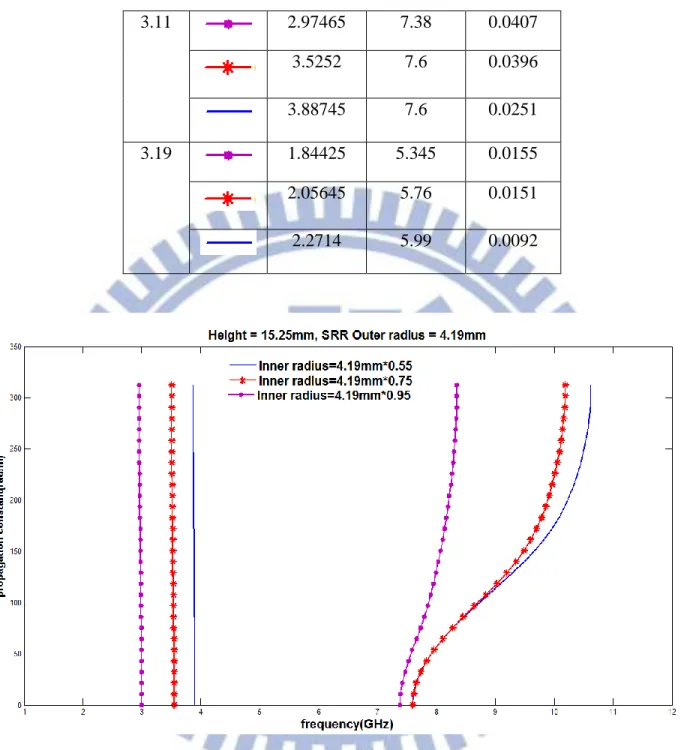
Figure 3.4 SRRs dimensions and Height effects on dispersion diagrams showing only outer radius of 4.19mm.
The height of the waveguide is 15.25mm and its width is 35 mm. The relative permittivity of each of the two dielectric side slabs is 4.5 with thickness 1.55mm.4.19 7.24mm, 0.55
, 0.55 0.087rad 0.087rad, represented in the figure in solid
16
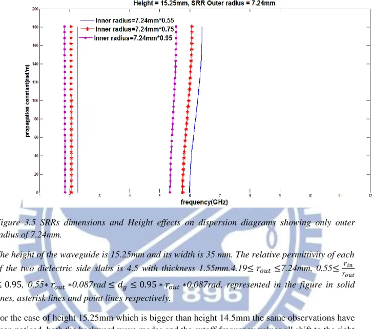
Figure 3.5 SRRs dimensions and Height effects on dispersion diagrams showing only outer radius of 7.24mm.
The height of the waveguide is 15.25mm and its width is 35 mm. The relative permittivity of each of the two dielectric side slabs is 4.5 with thickness 1.55mm.4.19 7.24mm, 0.55
, 0.55 0.087rad 0.087rad, represented in the figure in solid
lines, asterisk lines and point lines respectively.
For the case of height 15.25mm which is bigger than height 14.5mm the same observations have been noticed, both the backward wave modes and the cutoff frequency values all shift to the right side as their outer and inner diameters of the SRRs increases. As applied with heights 14.5mm both the outer and inner diameters of the SRRs rings with height 15.25mm have been also scale by factors [0.55 0.6 0.65 0.7 0.75 0.8 0.85 0.9 0.95]. Comparing the graphs of heights 14.5mm from figure a. to figure i. with the graphs of height 15.25mm from figure a) to figure i) respectively, more shifting to left with a height 15.25mm would be expected. When the SRRs rings are scale with the same scale factor but different heights the locations and positions of both the backward wave modes and the cutoff frequencies differs.
17
Table 3.4 Height = 16mm figures Legend Center
frequencies Cutoff frequencies Bandwidth 3.20 2.8394 7.21 0.034 3.3729 7.53 0.039 3.72275 7.53 0.022 3.28 1.5131 4.87 0.0056 1.7611 5.13 0.0058 1.97915 5.28 0.0017
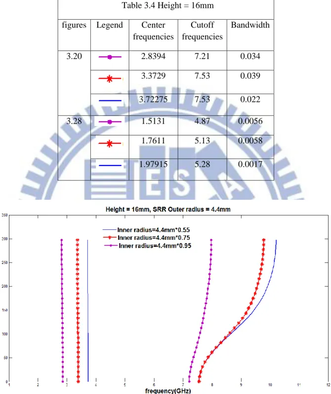
Figure 3.6 SRRs dimensions and Height effects on dispersion diagrams showing only outer radius of 4.4mm.
The height of the waveguide is 16mm and its width is 35 mm. The relative permittivity of each of the two dielectric side slabs is 4.5 with thickness 1.55mm.4.4 7.6mm, 0.55
18
0.55 0.087rad 0.087rad, represented in the figure in solid lines, asterisk lines and point lines respectively.
Figure 3.7SRRs dimensions and Height effects on dispersion diagrams showing only outer radius of 7.6mm.
The height of the waveguide is 16mm and its width is 35 mm. The relative permittivity of each of the two dielectric side slabs is 4.5 with thickness 1.55mm.4.4 7.6mm, 0.55
, 0.55 0.087rad 0.087rad, represented in the figure in solid lines,
asterisk lines and point lines respectively.
In this parametric study, the highest height was 16mm and comparing its dispersion diagrams with the dispersion diagrams of heights 14.5mm and 15.25mm, both the backward wave modes and their respective cutoff frequencies decrease towards the left side on the dispersion graphs though their respective SRRs rings have been scale with the same factors.
Waveguide width effects:
Waveguide width effects: The effect of waveguide width( ω = 35mm) variation on the modal dispersion have been investigated on three different heights, 14.5mm, 15.25mm and 16mm.The thickness (d = 1.55mm) of the dielectric slab on both side (2* d) of the waveguide have been maintained. The width between the two identical SRRs19
denoted here (a) centered within the two unit cells on both side (2*a) of the waveguide walls have been reduced to half (a). A parametric study of all the SRRs scale by factors [0.55, 0.6, 0.65, 0.7, 0.75, 0.8, 0.85, 0.9, 0.95] on all the three heights have been simulated but the figure below only shows the dispersion diagrams for the three different heights, the outer SRR diameter rings 0.95 times each of the three different heights of the waveguide, and the inner SRR diameter of rings 0.55 times the outer diameters of each height.
A rise in both backward wave modes and the ordinary modal cutoff frequencies have occurred with width a reduction. The backward wave mode on each of the three heights dispersion diagrams rise by shifting to the right side comparing with their dispersion diagrams when width (ω = 35mm) was maintained on all the three heights.
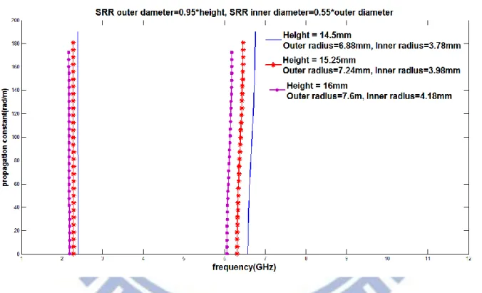
Figure 3.8 Height and Waveguide width effects on dispersion diagrams showing only outer diameter of 0.95*height and inner diameter of 0.55*outer diameter
14.5mm Height 16mm, with width 17.5 mm, , The relative permittivity of each of the two dielectric side slabs is 4.5 with thickness 1.55mm.0.55
0.55 0.087rad 0.087rad, represented in the figure in solid
20
Dielectric Slab d effects:
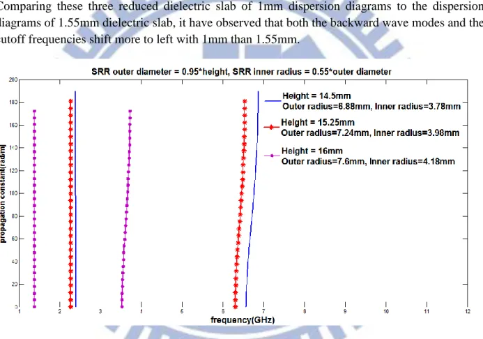
The thickness of the two dielectric slabs (2* d) loading on the two side walls of the rectangular waveguide have been studied. The two identical SRR arrays printed on the surface of both the dielectric slabs have been simulated reducing the thickness from 1.55mm to 1mm on both the side walls of the waveguide. Three different rectangular waveguides have investigated with all their SRRs scale by factors [0.55, 0.6, 0.65, 0.7, 0.75, 0.8, 0.85, 0.9, 0.95]. All designs of different waveguide heights exhibits backward modes on their dispersion graphs as expected. The figure below only shows their dispersion diagrams, the outer SRR diameter of the three rings 0.95 times each of the three different heights of the waveguide, and the inner SRR diameter of the three rings 0.55 times their outer diameters.Comparing these three reduced dielectric slab of 1mm dispersion diagrams to the dispersion diagrams of 1.55mm dielectric slab, it have observed that both the backward wave modes and the cutoff frequencies shift more to left with 1mm than 1.55mm.
Figure 3.9 Height and Dielectric slab effects on dispersion diagrams showing only outer diameter of 0.95*height and inner diameter of 0.55*outer diameter
14.5mm Height 16mm, with width 35mm, , The relative
permittivity of each of the two dielectric side slabs is 4.5 with thickness 1mm.0.55
0.55 0.087rad 0.087rad, represented in the figure in solid lines,
21
Relative permittivity
effects:
The substrate material with relative permittivity = 4.5 have changed to = 1. This reduction on the on the have affected the appearance of the backward wave modes on the three different heights 14.5mm, 15.25mm and 16mm simulation results. All the SRRs of the three heights scale by ring factors [0.55, 0.6, 0.65, 0.7, 0.75, 0.8, 0.85, 0.9, 0.95] have been simulated. The outer SRR diameter rings 0.95 times each of the three different heights and their inner SRR diameter of rings 0.55 times their respective outer diameters all possessed backward wave modes as shown in figure 3.10.Comparing the backward wave modes on each of the three heights dispersion diagrams where the relative permittivity have been changed to 1 with dispersion diagrams with relative permittivity = 4.5, the locations of the backward wave modes changes position at different locations decreasing to the left side and their ordinary cutoff frequencies locations were also influence with a smaller relative permittivity. The dispersion graphs of all the three heights with the rings scale by factor 0.95 and 0.55
Figure 3.10Relative permittivity ( )and Height effects on dispersion diagrams showing only outer diameter of 0.95*height and inner diameter of 0.55*outer diameter
14.5mm Height 16mm, with width 35 mm, , The relative permittivity of each of the two dielectric side slabs is 1 with thickness 1.55mm.0.55
22
0.55 0.087rad 0.087rad, represented in the figure in solid
lines, asterisk lines and point lines respectively.
II. CST Simulations
Computer Simulation Technology (CST) is a commercial microwave software tool used in the simulations and design of electromagnetic structures. The problem that usually found in CST design simulation is time consuming during the process and at end the results might not be good as expected. First of all before the start of the simulation process identical SRR loaded rectangular waveguide was drawn and various design configurations were generated.
The simulations of metamaterial element loaded waveguide structures are really timed consuming but previous authors have not paid much attention to this problem. My thesis work investigated a way of improving this problem to address long time consumption. Under the boundary conditions symmetry planes have set in particular directions; all to none field directions which involves all cases of fields, all to electric (electric fields are anti-symmetric whilst the magnetic fields are symmetric) or magnetic field directions (magnetic fields are anti-symmetric whilst the electric fields are anti-symmetric), one of the symmetry planes XZ plane electric or YZ plane magnetic or vice versa. The figure 3.11 below show the directions of symmetry planes under the boundary condition of CST design configuration structures.
23
Figure 3.11 Setting of symmetry planes under boundary conditions.
The first approach was setting all symmetry planes XZ and YZ to none fields directions and the simulation process took longer hours (total of 9 hours, 35mins and 55sec) but the modal pass-band appeared on the dispersion graphs. This way of setting the symmetry planes thought exhibited backward wave mode as expected but was unable to produce a fast enough simulation process. In the same design all symmetry planes XZ and YZ were set to electric fields directions the simulation was faster (total of 6 hours, 28mins and 14sec) consequently obtaining modal pass-band below the cutoff frequency. This approach of symmetry planes setting to all electric directions does not only speedy up the time but also exhibit modal pass-band. The other two settings of the symmetry planes was also fast enough but backward wave modes could not appear on the dispersion graphs.
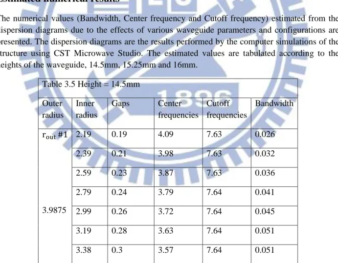
Estimated numerical results
The numerical values (Bandwidth, Center frequency and Cutoff frequency) estimated from the dispersion diagrams due to the effects of various waveguide parameters and configurations are presented. The dispersion diagrams are the results performed by the computer simulations of the structure using CST Microwave Studio. The estimated values are tabulated according to the heights of the waveguide, 14.5mm, 15.25mm and 16mm.
Table 3.5 Height = 14.5mm Outer radius Inner radius Gaps Center frequencies Cutoff frequencies Bandwidth 3.9875 2.19 0.19 4.09 7.63 0.026 2.39 0.21 3.98 7.63 0.032 2.59 0.23 3.87 7.63 0.036 2.79 0.24 3.79 7.64 0.041 2.99 0.26 3.72 7.64 0.045 3.19 0.28 3.63 7.64 0.051 3.38 0.3 3.57 7.64 0.051
24 3.58 0.31 3.42 7.6 0.06 3.78 0.33 3.12 7.5 0.047 4.35 2.39 0.21 3.76 7.56 0.021 2.61 0.23 3.66 7.56 0.027 2.82 0.25 3.56 7.56 0.032 3.04 0.27 3.48 7.56 0.034 3.26 0.28 3.43 7.56 0.039 3.48 0.3 3.32 7.56 0.042 3.69 0.32 3.28 7.58 0.044 3.91 0.34 3.16 7.58 0.046 4.13 0.36 3.14 7.25 0.038 4.7125 2.59 0.23 3.49 7.46 0.021 2.82 0.25 3.38 7.45 0.024 3.06 0.27 3.3 7.45 0.027 3.29 0.29 3.22 7.44 0.03 3.53 0.31 3.16 7.45 0.037 3.77 0.33 3.08 7.42 0.035 4 0.35 3.03 7.37 0.036 4.24 0.37 2.92 7.39 0.039 4.47 0.39 2.53 6.86 0.042 5.075 2.79 0.23 3.24 7.32 0.018 3.04 0.25 3.16 7.32 0.021 3.29 0.27 3.07 7.3 0.023 3.55 0.29 3 7.29 0.027
25 3.8 0.31 2.94 7.28 0.03 4.06 0.33 2.87 7.23 0.031 4.31 0.35 2.82 7.26 0.032 4.56 0.37 2.74 7.2 0.034 4.82 0.39 2.45 6.77 0.042 5.4375 2.99 0.26 3.03 7.16 0.016 3.26 0.28 2.94 7.13 0.018 3.53 0.31 2.87 7.11 0.019 3.8 0.33 2.79 7.08 0.023 4.07 0.36 2.74 7.08 0.024 4.35 0.38 2.68 7.02 0.028 4.62 0.4 2.63 7.01 0.027 4.89 0.43 2.57 6.945 0.029 5.16 0.45 2.29 6.43 0.037 5.8 3.19 0.28 2.85 6.96 0.014 3.48 0.3 2.76 6.93 0.017 3.77 0.33 2.7 6.9 0.019 4.06 0.35 2.63 6.86 0.019 4.35 0.38 2.57 6.81 0.023 4.64 0.4 2.52 6.77 0.025 4.93 0.43 2.47 6.72 0.023 5.22 0.45 2.41 6.65 0.026 5.51 0.48 2.08 5.895 0.024 3.38 0.3 2.67 6.74 0.012
26 6.1625 3.69 0.32 2.6 6.69 0.016 4 0.35 2.54 6.64 0.017 4.31 0.38 2.48 6.5975 0.019 4.62 0.4 2.42 6.535 0.025 4.93 0.43 2.37 6.495 0.02 5.23 0.46 2.33 6.43 0.023 5.54 0.48 2.28 6.38 0.027 5.85 0.51 1.96 5.6 0.022 6.525 3.58 0.31 2.53 6.48 0.011 3.91 0.34 2.46 6.43 0.014 4.24 0.37 2.39 6.38 0.016 4.56 0.4 2.33 6.32 0.017 4.89 0.43 2.28 6.255 0.018 5.22 0.45 2.23 6.195 0.019 5.54 0.48 2.2 6.155 0.019 5.87 0.51 2.14 6.07 0.019 6.19 0.54 1.96 5.62 0.018 6.8875 3.78 0.33 2.38 6.2 0.01 4.13 0.36 2.32 6.15 0.013 4.47 0.39 2.25 6.085 0.014 4.82 0.42 2.2 6.02 0.016 5.16 0.45 2.15 5.96 0.016 5.51 0.48 2.11 5.93 0.016 5.85 0.51 2.07 5.86 0.017
27
6.19 0.54 2.03 5.82 0.017 6.54 0.57 1.93 5.58 0.017
Figure 3.12Bandwidth versus inner radius. Each of the nine outer radii has nine varying inner radii
Table 3.5 shows height, Bandwidth and SRRs dimensions. The height of the waveguide is 14.5 mm and its width is 35 mm. The relative permittivity of each of the two dielectric side slabs is 4.5 with thickness 1.55mm. 3.98mm 6.8mm8, 0.55
0.95, 0.55 0.087rad
28
Figure 3.13 Center frequencies inner radius. Each of the nine outer radii has nine varying inner radii
Table 3.5 shows height, Center frequency and SRRs dimensions. The height of the waveguide is 14.5 mm and its width is 35 mm. The relative permittivity of each of the two dielectric side slabs
is 4.5 with thickness 1.55mm. 3.98mm 6.8mm8, 0.55
0.95, 0.55 0.087rad
29
Figure 3.14Cutoff frequencies versus inner radius. Each of the nine outer radii has nine varying inner radii
Table 3.5 shows height, Cutoff frequencies and SRRs dimensions. The height of the waveguide is 14.5 mm and its width is 35 mm. The relative permittivity of each of the two dielectric side slabs
is 4.5 with thickness 1.55mm. 3.98mm 6.8mm8, 0.55 0.95, 0.55 0.087rad 0.087rad Table 3.6 Height = 15.25mm Outer radius Inner radius Gaps Center frequencies Cutoff frequencies Bandwidth 4.19375 2.3065625 0.20 3.88745 7.6 0.0251 2.51625 0.22 3.7977 7.6 0.0286 2.7259375 0.24 3.6908 7.6 0.0344 2.935625 0.26 3.6305 7.6 0.039
30 3.1453125 0.27 3.5252 7.6 0.0396 3.355 0.29 3.4553 7.6 0.0454 3.5646875 0.31 3.40175 7.6 0.0465 3.77435 0.33 3.26885 7.58 0.0482 3.9840625 0.35 2.97465 7.38 0.0407 4.575 2.51625 0.22 3.58905 7.5 0.0219 2.745 0.24 3.4923 7.5 0.0254 2.97375 0.26 3.3934 7.5 0.0292 3.2025 0.28 3.31945 7.5 0.0346 3.43125 0.30 3.2467 7.5 0.0346 3.66 0.32 3.17225 7.5 0.0355 3.88875 0.34 3.13545 7.5 0.0391 4.1175 0.36 3.01525 7.45 0.0395 2.7259375 0.38 2.7292 7.04 0.0316 4.95625 2.97375 0.24 3.32365 7.38 0.0127 3.2215625 0.26 3.22175 7.38 0.0205 3.469375 0.28 3.1479 7.36 0.0242 3.7171875 0.30 3.0697 7.36 0.0286 3.965 0.32 3.00805 7.34 0.0319 4.2128125 0.35 2.93555 7.32 0.0329 4.460625 0.37 2.89315 7.32 0.0337 4.7084375 0.39 2.78455 7.26 0.0349 2.7259375 0.41 2.416 6.63 0.0339 2.935625 0.26 3.09605 7.225 0.0159
31 5.3375 3.2025 0.28 3.0071 7.2 0.0178 3.469375 0.30 2.9257 7.18 0.0206 3.73625 0.33 2.86025 7.16 0.0235 4.003125 0.35 2.8 7.15 0.024 4.27 0.37 2.74015 7.12 0.0297 4.536875 0.40 2.69295 7.1 0.0301 4.80375 0.42 2.61205 7.02 0.0319 5.070625 0.44 2.33855 6.53 0.0349 5.71875 3.1453125 0.27 2.88935 7.02 0.0133 3.43125 0.30 2.80805 6.99 0.0159 3.7171875 0.32 2.7346 6.96 0.0188 4.003125 0.35 2.6702 6.92 0.0216 4.2890625 0.37 2.60825 6.87 0.0235 4.575 0.40 2.55955 6.84 0.0249 4.8609375 0.42 2.5065 6.79 0.026 5.146875 0.45 2.44605 6.795 0.0269 5.4328125 0.47 2.11845 5.92 0.0271 6.1 3.355 0.29 2.71655 6.795 0.0149 3.66 0.32 2.6363 6.75 0.0148 3.965 0.35 2.5712 6.72 0.0176 4.27 0.37 2.5054 6.66 0.0192 4.575 0.40 2.4492 6.6 0.0206 4.88 0.43 2.4008 6.56 0.0224 5.185 0.45 2.3524 6.49 0.0232
32 5.49 0.48 2.30635 6.44 0.0233 5.795 0.51 1.9892 5.65 0.0226 6.48125 3.5646875 0.31 2.5575 6.55 0.0129 3.8875 0.34 2.4862 6.5 0.0136 4.2128125 0.37 2.4228 6.44 0.0164 4.536875 0.40 2.3683 6.38 0.0166 4.8609375 0.42 2.3064 6.31 0.0192 5.185 0.45 2.2578 6.26 0.0204 5.5090625 0.48 2.22385 6.22 0.0203 5.833125 0.51 2.1698 6.14 0.0204 6.1571875 0.54 1.9921 5.65 0.0178 6.8625 3.774375 0.33 2.4161 6.28 0.02 4.1175 0.36 2.34625 6.23 0.0115 4.460625 0.39 2.28095 6.16 0.0141 4.80375 0.42 2.22205 6.08 0.0159 5.146875 0.45 2.1739 6.02 0.0162 5.49 0.48 2.14145 5.99 0.0171 5.833125 0.51 2.0958 5.91 0.0184 6.17625 0.54 2.06275 5.87 0.0185 6.519375 0.57 1.87585 5.67 0.0163 7.24375 3.9840625 0.35 2.2714 5.99 0.0092 4.34625 0.38 2.21545 5.955 0.0111 4.7084375 0.41 2.15005 5.88 0.0119 5.070625 0.44 2.098475 5.81 0.01355
33 5.4328125 0.47 2.05645 5.76 0.0151 5.795 0.51 2.0164 5.7 0.0151 6.1571875 0.54 1.97325 5.63 0.0155 6.519375 0.57 1.93605 5.58 0.0159 6.8815625 0.60 1.84425 5.345 0.0155
Figure 3.15 Bandwidth versus inner radius. Each of the nine outer radii has nine varying inner radii
Table 3.6 shows height, bandwidth and SRRs dimensions. The height of the waveguide is 15.25 mm and its width is 35 mm. The relative permittivity of each of the two dielectric side slabs is 4.5
with thickness 1.55mm. 4.19mm 7.24mm8, 0.55
0.95, 0.55 0.087rad
34
Figure 3.16 Center frequencies versus inner radius. Each of the nine outer radii has nine varying inner radii
Table 3.6 shows height, Center frequencies and SRRs dimensions. The height of the waveguide is 15.25 mm and its width is 35 mm. The relative permittivity of each of the two dielectric side slabs
is 4.5 with thickness 1.55mm. 4.19mm 7.24mm8, 0.55
0.95, 0.55 0.087rad
35
Figure 3.17 Cutoff frequencies versus inner radius. Each of the nine outer radii has nine varying inner radii
Table 3.6 shows height, Cutoff frequencies and SRRs dimensions. The height of the waveguide is 15.25 mm and its width is 35 mm. The relative permittivity of each of the two dielectric side slabs
is 4.5 with thickness 1.55mm. 4.19mm 7.24mm8, 0.55
0.95, 0.55 0.087rad
36 Table 3.7 Height = 16mm Outer radius Inner radius Gaps Center frequencies Cutoff frequencies Bandwidth 4.4 2.42 0.21 3.72 7.56 0.022 2.64 0.23 3.62 7.56 0.026 2.86 0.25 3.52 7.55 0.031 3.08 0.27 3.46 7.56 0.035 3.3 0.29 3.37 7.53 0.034 3.52 0.31 3.29 7.55 0.04 3.74 0.33 3.25 7.57 0.037 3.96 0.35 3.11 7.52 0.044 4.18 0.36 2.83 7.21 0.039 4.8 2.64 0.23 3.42 7.44 0.018 2.88 0.25 3.32 7.44 0.022 3.12 0.27 3.24 7.43 0.026 3.36 0.29 3.16 7.42 0.03 3.6 0.31 3.1 7.42 0.032 3.84 0.33 3.02 7.395 0.032 4.08 0.36 2.99 7.415 0.036 4.32 0.38 2.87 7.36 0.036 4.56 0.4 2.49 6.78 0.036 2.86 0.25 3.17 7.28 0.021 3.12 0.27 3.07 7.26 0.019 3.38 0.29 3 7.25 0.024
37 5.2 3.64 0.32 2.93 7.24 0.026 3.9 0.34 2.87 7.23 0.027 4.16 0.36 2.8 7.19 0.03 4.42 0.39 2.76 7.19 0.028 4.68 0.41 2.68 7.12 0.031 4.94 0.43 2.4 6.66 0.039 5.6 3.08 0.27 2.95 7.09 0.015 3.36 0.29 2.86 7.14 0.019 3.64 0.32 2.79 7.04 0.019 3.92 0.34 2.72 7 0.022 4.2 0.37 2.67 6.98 0.023 4.48 0.39 2.61 6.93 0.025 4.76 0.41 2.56 6.91 0.025 5.04 0.44 2.49 6.83 0.029 5.32 0.46 2.19 6.21 0.03 6 3.3 0.29 2.76 6.86 0.013 3.6 0.31 2.67 6.82 0.017 3.9 0.34 2.61 6.78 0.018 4.2 0.37 2.55 6.74 0.02 4.5 0.39 2.48 6.67 0.021 4.8 0.42 2.43 6.63 0.022 5.1 0.44 2.39 6.565 0.023 5.4 0.47 2.34 6.52 0.024 5.7 0.5 2.02 5.72 0.024
38 6.4 3.52 0.31 2.59 6.61 0.012 3.84 0.33 2.51 6.55 0.013 4.16 0.36 2.45 6.5 0.016 4.48 0.39 2.38 6.43 0.016 4.8 0.42 2.33 6.37 0.018 5.12 0.45 2.28 6.33 0.02 5.44 0.47 2.24 6.28 0.02 5.76 0.5 2.18 6.19 0.019 6.08 0.53 2.01 5.71 0.019 6.8 3.74 0.33 2.42 6.33 0.012 4.08 0.36 2.37 6.27 0.013 4.42 0.39 2.3 6.203 0.014 4.76 0.41 2.24 6.12 0.014 5.1 0.44 2.19 6.07 0.016 5.44 0.47 2.16 6.035 0.018 5.78 0.5 2.11 5.96 0.018 6.12 0.53 2.08 5.91 0.019 6.46 0.56 1.88 5.42 0.016 7.2 3.96 0.35 2.28 6.03 0.009 4.32 0.38 2.23 5.99 0.011 4.68 0.41 2.16 5.91 0.015 5.04 0.43 2.11 5.84 0.014 5.4 0.47 2.06 5.8 0.014 5.76 0.5 2.03 5.73 0.015
39 6.12 0.53 1.98 5.665 0.016 6.48 0.56 1.95 5.63 0.015 6.84 0.6 1.85 5.38 0.014 7.6 4.18 0.36 1.97 5.28 0.0017 4.56 0.4 1.92 5.26 0.003 4.94 0.43 1.86 5.21 0.007 5.32 0.46 1.8 5.17 0.005 5.7 0.5 1.76 5.13 0.005 6.08 0.53 1.7 5.07 0.005 6.46 0.56 1.65 5.02 0.005 6.84 0.6 1.6 5.01 0.005 7.22 0.63 1.51 4.87 0.005
40
Figure 3.18 Bandwidth versus inner radius. Each of the nine outer radii has nine varying inner radii
Table 3.7 shows height, bandwidth and SRRs dimensions. The height of the waveguide is 16 mm and its width is 35 mm. The relative permittivity of each of the two dielectric side slabs is 4.5 with thickness 1.55mm. 4.4mm 7.6mm8, 0.55
0.95, 0.55 0.087rad
0.087rad
Figure 3.19 Center frequencies versus inner radius. Each of the nine outer radii has nine varying inner radii
Table 3.7 shows height, Center frequencies and SRRs dimensions. The height of the waveguide is 16 mm and its width is 35 mm. The relative permittivity of each of the two dielectric side slabs is 4.5 with thickness 1.55mm. 4.4mm .6mm8, 0.55
0.95, 0.55 0.087rad
41
Figure 3.20 cutoff frequencies versus inner radius. Each of the nine outer radii has nine varying inner radii
Table 3.7 shows height, Cutoff frequencies and SRRs dimensions. The height of the waveguide is 16 mm and its width is 35 mm. The relative permittivity of each of the two dielectric side slabs is 4.5 with thickness 1.55mm. 4.4mm 7.6mm8, 0.55
0.95, 0.55 0.087rad
0.087rad
III. Map design application
A map has been designed to see the overlap of the parameters on the dispersion graphs. The rectangular waveguide dimensions are as follows W = 35mm, h = 14.5mm and 16mm, the material on which the SRR were printed is = 4.5 and width a thickness of 1.55mm. Origin 75 graphical software have been use to present this overlap with the designed map applications. The SRRs dimensions; outer and inner radii, gaps have been tabulated in table 3.4 and 3.6 above. The goal of the optimization is to achieve an overlapping area of all the parameters on the dispersion graphs. Eigenmode solver of CST Microwave Studio was used to compute the dispersion diagrams for the solution evaluations.
42
Firstly, map design application for optimization for the height 16mm whilst keeping gaps 0.21 and 0.36 constantly have been performed but the rest of the parameters as indicated on table 2 remain unchanged. The SRRs gap 0.21 and 0.36 has later been mapped as shown in the following figures.
Figure 3.21 Map design graphs of gaps 0.21 and 0.36, Bandwidth versus inner radius showing their respective outer and inner radii
The height of the waveguide is 16mm its width is 35 mm. The relative permittivity of each of the two dielectric side slabs is 4.5 with thickness 1.55mm. 4.4mm 7.6mm, 0.55
0.95,
0.55
0.95, 0.55 0.087rad 0.087rad.SRRs gaps are 0.21and 0.36, represented in the figure in black point lines and red point lines respectively.
43
Figure 3.22 Map design graphs of gaps 0.21 and 0.36, center frequencies versus inner radius showing their respective outer and inner radii
The height of the waveguide is 16mm its width is 35 mm. The height of the waveguide is 16mm its width is 35 mm. The relative permittivity of each of the two dielectric side slabs is 4.5 with
thickness 1.55mm. 4.4mm 7.6mm, 0.55
0.95, 0.55
0.95, 0.55
0.087rad 0.087rad.SRRs gaps are 0.21and 0.36, represented in the
44
Figure 3.23 Map design graphs of gaps 0.21 and 0.36, cutoff frequencies versus inner radius showing their respective outer and inner radii
The height of the waveguide is 16mm its width is 35 mm. The relative permittivity of each of the two dielectric side slabs is 4.5 with thickness 1.55mm. 4.4mm 7.6mm, 0.55
0.95,
0.55
0.95, 0.55 0.087rad 0.087rad.SRRs gaps are 0.21and 0.36, represented in the figure in black point lines and red point lines respectively.
Finally the plots of height 14.5 and plots of 16mm have also been map together which includes their respective SRRs parameters.
45
Figure 3.24 Map design graphs of heights 14.5mm and 16mm, Bandwidth versus inner radius
showing their respective outer and inner radii
Table 3.5 and 3.7 shows heights, bandwidth and SRRs dimension. 14.5mm Height 16mm, with
width 35 mm, , The relative permittivity of each of the two dielectric side slabs is 4.5 with thickness 1.55mm.0.55
0.55 0.087rad
0.087rad, represented in the figure black point lines and red point lines
46
Figure 3.25 Map design graphs of heights 14.5mm and 16mm, Center frequency versus inner showing their respective outer and inner radii
Table 3.5 and 3.7 shows heights, bandwidth and SRRs dimension. 14.5mm Height 16mm, with
width 35 mm, , The relative permittivity of each of the two dielectric side slabs is 4.5 with thickness 1.55mm.0.55
0.55 0.087rad
0.087rad, represented in the figure black point lines and red point lines
47
Figure 3.26 Map design graphs of heights 14.5mm and 16mm, Cutoff frequency versus inner showing their respective outer and inner radii
Table 3.5 and 3.7 shows heights, bandwidth and SRRs dimension. 14.5mm Height 16mm, with
width 35 mm, , The relative permittivity of each of the two dielectric side slabs is 4.5 with thickness 1.55mm.0.55
0.55 0.087rad
0.087rad, represented in the figure black point lines and red point lines
respectively.
Though my design configurations have not been fabricated to take measurements and compare the measurement results with the CST simulation dispersion diagrams. A map design could be used to verify my results with similar results with both simulations and measurement results. Two examples from the dispersion diagram [7] figure 2.4 and my results have been verified using design map.
48
Example 1
= 7.6mm, = 6.4mm, = 1.4mm
Data from CST Dispersion diagrams
From figure 2.4 From Map design Bandwidth Not given 5MHz Center frequency 1.8GHz 1.7GHz Cutoff frequency 3.6GHz 5.0GHz
Example 2
= 6.4mm, = 5.12mm, = 1.4mm
Data from CST Dispersion diagrams
From figure 2.4 From Map design Bandwidth Not given 13MHz Center frequency 2.4GHz 2.5GHz Cutoff frequency 3.7GHz 6.7GHz
IV. Polynomial curve fitting model
A commercial microwave solver CST tool was used for the numerical investigations. The numerical data have been modeled in a polynomial curve fitting to see the behavior of these parameters. The graphical expressions analyze the behavior of the backward wave and the cutoff frequencies with the variations of certain parameters in the dispersion diagram of SRR loaded rectangular waveguide. The estimated numerical data (bandwidths, center frequencies and cutoff frequencies) and the calculated data (outer radius and inner radius) have been stored in two different vectors respectively and modeled as a 5th degree polynomial curve fitting. The 5th degree polynomial expansion of a function y = f(x) takes the following form.
49
Where Y= [ , , ……, ] are the estimated numerical data
X= [ , , ……, ] are real calculated values of the outer radius and inner radius of the of the SRR scale by factors ranging from 0.55 to 0.95.
From polynomial curve fitting graphs of heights 14.5mm, 15.25mm and 16mm have been presented below. It have been noticed from all these graphs that the heights of the waveguide have effects on the backward wave, Bandwidths, Center frequencies and the cutoff frequencies. As the outer radius and inner radius of the SRRs increases, the Bandwidths, Center frequencies and the cutoff frequencies value decreases.
Figure 3.27 show the polynomial curve-fitting modeling of figure 3.11.
Table 3.5 shows height, Bandwidth and SRRs dimensions. The height of the waveguide is 14.5 mm and its width is 35 mm. The height of the waveguide is 14.5 mm and its width is 35 mm. The relative permittivity of each of the two dielectric side slabs is 4.5 with thickness 1.55mm. 3.98mm 6.8mm8, 0.55 0.087rad 0.087rad, represented in the figure in green circles lines. Blue point lines in the figure are test values.
50
Figure 3.28 Polynomial curve-fitting modeling of figure 3.12.
Table 3.5 shows height, center frequencies and SRRs dimensions. The height of the waveguide is 14.5 mm and its width is 35 mm. The height of the waveguide is 14.5 mm and its width is 35 mm. The relative permittivity of each of the two dielectric side slabs is 4.5 with thickness 1.55mm. 3.98mm 6.8mm8, 0.55 0.087rad 0.087rad, represented in the figure in green circles lines. Blue point lines in the figure are test values.
51
Figure 3.29 Polynomial curve-fitting modeling of figure 3.13.
Table 3.5 shows height, cutoff frequencies and SRRs dimensions. The height of the waveguide is 14.5 mm and its width is 35 mm. The height of the waveguide is 14.5 mm and its width is 35 mm. The relative permittivity of each of the two dielectric side slabs is 4.5 with thickness 1.55mm. 3.98mm 6.8mm8, 0.55 0.087rad 0.087rad, represented in the figure in green circles lines. Blue point lines in the figure are test values.
52
Figure 3.30 Polynomial curve-fitting modeling of figure 3.14.
Table 3.6 shows height, bandwidth and SRRs dimensions. The height of the waveguide is 15.25 mm and its width is 35 mm. The relative permittivity of each of the two dielectric side slabs is 4.5
with thickness 1.55mm. 4.19 7.24mm, 0.55
0.95, 0.55 0.087rad
0.087rad, represented in the figure in green circles lines. Blue point lines in the
53
Figure 3.31 Polynomial curve-fitting modeling of figure 3.15.
Table 3.6 shows height, center frequencies and SRRs dimensions. . The height of the waveguide is 15.25 mm and its width is 35 mm. The relative permittivity of each of the two dielectric side slabs is 4.5 with thickness 1.55mm. 4.19 7.24mm, 0.55
0.95, 0.55
0.087rad 0.087rad, represented in the figure in green circles lines.
Blue point lines in the figure are test values
54
Figure 3.32 Polynomial curve-fitting modeling of figure 3.16.
Table 3.6 shows height, cutoff frequencies and SRRs dimensions. The height of the waveguide is 15.25 mm and its width is 35 mm. The relative permittivity of each of the two dielectric side slabs
is 4.5 with thickness 1.55mm. 4.19 7.24mm, 0.55
0.95, 0.55 0.087rad
0.087rad, represented in the figure in green circles lines. Blue point lines in
the figure are test values
55
Figure 3.33 Polynomial curve-fitting modeling of figure 3.17.
Table 3.7 shows height, bandwidth and SRRs dimensions. The height of the waveguide is 16 mm and its width is 35 mm. The relative permittivity of each of the two dielectric side slabs is 4.5 with thickness 1.55mm. 4.4mm , 0.55
0.55 0.087rad
0.087rad, represented in the figure in green circles lines. Blue point lines in the
figure are test values.
Polynomial coefficients of 5th degree modeling for bandwidth of height 16mm
design configurations
Polycoeff ( ) -0.0391 0.6337 -4.0741 12.9677 -20.4108 12.7214 Polycoeff ( ) -0.0454 0.8508 -6.3346 23.4128 -42.9325 31.2506 Polycoeff -0.0023 0.0573 -0.5430 2.4535 -5.3360 4.515156 ( ) Polycoeff ( ) -0.0006 0.0123 -0.0919 0.3291 -0.5482 0.3385 Polycoeff ( ) 0.0012 -0.0289 0.2708 -1.2557 2.8926 -2.6348 Polycoeff ( ) 0.0005 -0.0108 0.0954 -0.4085 0.8543 -0.6891 Polycoeff ( ) 0.0002 -0.0074 0.0868 -0.4883 1.3342 -1.4123 Polycoeff ( ) -0.0002 0.0047 -0.0409 0.1594 -0.2483 0.0685 Polycoeff ( ) 0.0001 -0.0021 0.0280 -0.1910 0.6490 -0.8687
57
Figure 3.34 Polynomial curve-fitting modeling of figure 3.18.
Table 3.7 shows height, center frequencies and SRRs dimensions. The height of the waveguide is 16 mm and its width is 35 mm. The relative permittivity of each of the two dielectric side slabs is 4.5 with thickness 1.55mm. 4.4mm , 0.55
0.55 0.087rad
0.087rad, represented in the figure in green circles lines. Blue point lines in
the figure are test values.
Polynomial coefficients of 5th degree modeling for center frequencies of height 16mm design configurations Polycoeff ( ) -0.3462 5.3813 -33.2860 102.4632 -157.4059 100.4960 Polycoeff ( ) -0.4301 7.3555 -49.9878 168.8038 -283.6373 193.3609 Polycoeff -0.2230 4.1667 -30.9496 114.2803 -210.0827 157.1690
58 ( ) Polycoeff ( ) -0.1708 3.4289 -27.3495 108.3852 -213.6892 170.8119 Polycoeff ( ) -0.1617 3.4999 -30.0908 128.4401 -272.4209 232.6212 Polycoeff ( ) -0.0407 0.9300 -8.4379 38.0580 -85.5732 79.5051 Polycoeff ( ) -0.1372 3.4748 -34.9040 173.6943 -428.2151 420.8552 Polycoeff ( ) -0.0089 0.2187 -2.1282 10.2524 -24.6425 26.1358 Polycoeff ( ) -0.0085 0.2323 -2.5318 13.7005 -36.9568 41.8750
59
Figure 3.35 Polynomial curve-fitting modeling of figure 3.19.
Table 3.7 shows height, cutoff frequencies and SRRs dimensions. The height of the waveguide is 16 mm and its width is 35 mm. The relative permittivity of each of the two dielectric side slabs is 4.5 with thickness 1.55mm. 4.4mm , 0.55
0.55 0.087rad
0.087rad, represented in the figure in green circles lines. Blue point lines in
the figure are test values.
Polynomial coefficients of 5th degree modeling for cutoff frequencies of height
16mm design configurations
Polycoeff ( ) -0.6033 9.3704 -57.7731 176.7393 -268.3118 169.2970 Polycoeff ( ) -0.8232 14.1037 -95.9405 323.8563 -542.4733 368.1735 Polycoeff -0.4397 8.2141 -60.9588 224.6002 -410.8268 305.723960 ( ) Polycoeff ( ) -0.2347 4.4722 -33.6615 124.9923 -228.9393 172.6092 Polycoeff ( ) -0.4102 8.8546 -75.8713 322.5217 -680.2258 576.3869 Polycoeff ( ) -0.1356 3.0847 -27.8522 124.8019 -277.7099 252.2823 Polycoeff ( ) -0.1000 2.4090 -23.0418 109.3484 -257.6905 247.7892 Polycoeff ( ) -0.0323 0.8197 -8.2337 40.9654 -101.1296 105.3253 Polycoeff ( ) -0.0222 0.6117 -6.6621 35.9114 -95.8964 106.8781
CHAPTER 4
CONCLUSIONS
I.Summary
The specify objective of this study was as follows:
To investigate the extent to which the appearance of backward wave mode exist within the narrow pass-band of the waveguide cutoff frequency can be obtained. To determine the conditions under which the modal pass-band and the cutoff
frequency would appear and position on the dispersion graphs.
To investigate how the design simulation can be speed up by using CST software tool.
61
As already stated at above the study was to examine the factors affecting the appearance of the modal pass-band on SRR loaded rectangular waveguide. The investigation was able to show the influences and effects of the design involved parameters on the dispersion diagrams. Understanding of the specify study above will have no doubt contribute significantly in the research of waveguide with SRR metamaterials. In order to obtain modal pass-band below the waveguide cutoff frequency the height of the waveguide had great impact to this. The findings obtained in case of different heights whilst maintaining the rest of the parameters in the design configurations does not only indicated the influences locations of the backward wave mode but also affects the presence/absence of the pass-band below the cutoff frequency. The results of this specify parameter (heights) shows small heights ranging from 10mm and 16mm support an environment for backward travelling waves. Only dispersion diagrams of heights ranging from heights 14.5mm to 16mm have presented. The SRR inserted in the waveguide fails to exhibits negative permeability which should be have been combined with the negative permittivity of the dominant TE mode to obtain the pass-band. This shows that in any SRR rectangular waveguide the height of the waveguide should be better chosen in order to obtain backward wave mode as expected.
As the main goal of SRR loaded rectangular waveguide configuration is to obtained backward wave mode, the understanding of SRR element is of great importance to sustain pass-band in all the dispersion diagrams computed. There the dimensions of the SRR inclusion was characterize at different scaling factors. Fixing the outer SRR radius and varying the inner SRR radius by SRR scale factor the design configuration with small heights is likely to create pass-band on the dispersion graphs. The modal pass-band position decreases with an increase in SRR dimension by scale factors.
The research has shown how width reduction on the design has effects on the backward wave mode. Width increment or reduction has an influence on the position of both backward wave mode and the cutoff frequency. Backward wave mode and the cutoff frequency moves to the right side or left side when the design width parameter reduces and increase respectively. The results also provide that design configurations which exhibit pass-band below the cutoff frequency can still pass-band below the waveguide in the width reduction on the dispersion diagram. The same design configurations with different dielectric slab was also determined whether or not increment or reduction of dielectric slab thickness has influence and effects on the dispersion diagrams. It have been proved that here that the dielectric slab has effects and influences on the appearance and the position of the backward wave mode.
The used of CST simulation software required appropriate methods to speed up the simulation process. However the approach use was the setting of symmetry planes under the boundary conditions of the design structures. Various symmetry planes includes: YZ plane and XZ plane all electric directions, YZ plane and XZ plane all in magnetic field directions, YZ plane and XZ plane all none field directions, either YZ plane or XZ plane are set to electric-magnetic or
![Figure 2.1 Rectangular waveguide structures [13]](https://thumb-ap.123doks.com/thumbv2/9libinfo/8234353.171082/10.918.106.791.109.1003/figure-rectangular-waveguide-structures.webp)
![Figure 2.4.Dispersion diagram of the proposed waveguide with SRR of identical sizes on both sides (solid lines) [7]](https://thumb-ap.123doks.com/thumbv2/9libinfo/8234353.171082/15.918.107.814.102.902/figure-dispersion-diagram-proposed-waveguide-identical-sizes-sides.webp)