國 立 交 通 大 學
電 子 工 程 學 系 電 子 研 究 所
碩 士 論 文
具有適當密度與元件結構之奈米碳管之場發射特性
最佳化
Optimization for the Field Emission Properties of
Carbon Nanotubes with Proper Densities and
Device Structures
研 究 生:許 鈞 凱
指導教授:鄭 晃 忠 博士
具有適當密度與元件結構之奈米碳管之場發射特性最佳化
Optimization for the Field Emission Properties of Carbon
Nanotubes with Proper Densities and Device Structures
研 究 生:許鈞凱 Student: Jiun-Kai Shiu
指導教授:鄭晃忠 博士 Advisor: Dr. Huang-Chung Cheng
國 立 交 通 大 學
電子工程學系 電子研究所碩士班
碩士論文
A Thesis
Submitted to Department of Electronics Engineering & Institute of Electronics College of Electrical and Computer Engineering
National Chiao Tung University In Partial Fulfillment of the Requirements
for the Degree of Master in
Electronics Engineering 2006
Hsinchu, Taiwan, Republic of China
具有適當密度與元件結構之奈米碳管之場發射特
性最佳化
研究生: 許鈞凱 指導教授: 鄭晃忠 博士
國立交通大學電子工程學系 電子研究所碩士班
摘 要
利用熱化學氣相沉積系統成長出來的奈米碳管的密度依舊太高而導致因
遮蔽效應而造成場發射電流密度下降和起始電場上升。在此論文中,我們提
出了三種新穎的密度控制方法去控制奈米碳管的密度進而改善場發射特性,
其中包括了兩種薄的鈦覆蓋層的製程和一個鐵和鈦共鍍的製程。對於沒有前
處理而蓋薄的鈦覆蓋層的方法,其場發射特性不好。對於前處理完後蓋薄的
鈦覆蓋層的方法,當奈米碳管的密度由 2.8x10
8cm
-2下降到 2.8x10
7cm
-2時,
在 6 V/μm 的電場下其場發射電流密度從 11.12 mA/cm
2增加到 97.6 mA/cm
2,
起始電場從 3.786 V/μm下降到 2.5 V/μm。然而,從發光的圖像來看,其均
勻度依舊沒有被改善。對於鐵和鈦共鍍的方法,由於在濺鍍的過程中鐵和鈦
的原子是均勻分佈在其中,所以可以得到一個比較均勻的催化金屬膜。由此
可知,共鍍的技巧將會改善奈米碳管的均勻度並期待在未來大尺寸且高解析
度奈米碳管場發射顯示器的誕生。除此之外,我們提出了兩種機制來解釋這
三種密度控制的現象。
為了符合場發射顯示器低電壓操作的目的,我們利用一控制閘極來製造奈
米碳管之發射三極元件。然而,傳統的三極結構 (二氧化矽-多晶矽) 有一個
很嚴重的問題,那就是低發射效率,大概是 1.23 % 左右。因此我們在傳統的
三極結構中加入了一個氮化矽絕緣層來克服這個問題。從模擬來看,當加入
了氮化矽絕緣層之後,閘極附近的電位線有變疏的現象,而且電位線的分佈
也因此被改變。另一方面,氮化矽絕緣層將會阻擋部分的電子發射到閘極端
因此使閘極的漏電流下降。綜合上述的原因,這將會使得更多的電子穿越過
閘極的區域而到達陽極端,因此場發射效率將會被提升。如果氮化矽絕緣層
是加在多晶矽的上方的話,其發射效率將會增加到 8.56 %,而且也因為維持
了閘極的控制力,故使得陽極的場發射電流密度高達 5.44 mA/cm
2.
Optimization for the Field Emission Properties of
Carbon Nanotubes with Proper Densities and
Device Structures
Student : Jiun-Kai Shiu Advisor : Dr. Huang-Chung Cheng
Department of Electronic Engineering &
Institute of Electronics
National Chiao Tung University
Abstract
The density of CNTs synthesized by thermal CVD was still too high to reduce the field emission current density and ascend the turn-on field due to the screening effects. In this thesis, three novel methods including two thin Ti capping layer processes and a co-deposition of Ti and Fe process were introduced to improve the field emission properties via controlling the density of CNTs. For the thin Ti capping layer without pre-treatment, the field emission properties were poor. For the thin Ti capping layer with pre-treatment, the field emission current density improved from 11.12 mA/cm2 to 97.6 mA/cm2 at the electric field of 6 V/μm and the turn-on field decreased from 3.786 V/μm to 2.5 V/μm when the density of CNTs diminished from 2.8x10⁸ emitter/cm2 to 2.8x10⁷ emitter/cm2. However, the uniformity was not still improved from the luminescent images. For the co-deposition of Fe and Ti, the atoms of Fe and Ti were uniform
distribution during the sputtering, so it could obtain a more uniform catalytic metal layer. This showed the co-deposition technique could improve the uniformity of CNTs and expect that a large size field emission display with higher resolution would be fabricated in the future. Besides, two mechanisms were put forward to expound these phenomena of three density control methods. The CNTs triode structures with an extraction gate were proposed to achieve the low voltage modulation. However, the traditional triode structure (oxide-poly) had a serious problem of low efficiency (1.23 %). In order to overcome this problem, the traditional triode structure adding a nitride insulting layer was introduced. From the simulations, the electrostatic potential near the gate electrode was getting sparse and the distribution of electrostatic potential was also changed after adding a nitride insulting layer. On the other hand, the nitride insulting layer would block some electrons emitting to the gate electrode hence cause the reduction of gate leakage current. Sum up these reasons, it would make more electrons to pass through the gate holes and collect by the anode hence cause the increase of efficiency. If the nitride insulting layer was acceding above the poly-Si, the efficiency was added to 8.56 % and the emission anode current density was about 5.44 mA/cm2 which might result from the keeping of gate controllability.
誌 謝
首先要感謝國立交通大學所有教導過我的老師,尤其是我的指導教授-鄭晃忠博 士,謝謝老師在研究上的熱心指導和鼓勵,使我獲益良多,也讓我順利完成了碩士學位; 在待人處事上,老師謙恭溫和的模範,也成為我心中的典範。再來要感謝賴瑞霖學長這 一年多來亦師亦友的教導,不斷地解決我在實驗上的問題,而且還幫我的論文作最後的 校稿,使我殘破不堪的英文終有完整的一天。其次,要感謝交通大學奈米中心 (NFC) 和 國家毫微米實驗室 (NDL) 提供完善的實驗設備,尤其是要感謝奈米中心的技術人員-徐 秀鑾小姐、黃月美小姐、陳聯珠小姐、林素珠小姐、范秀蘭小姐、陳悅婷小姐、葉雙得 先生、胡進章先生和何惟梅小姐,他們在實驗設備及維護上給予最大的支持與協助,使 我的研究得以順利完成。 感謝從大學到研究所來的難兄難弟,翰忠和旭信,無論是實驗或是生活上,都豐富 了我的求學生涯。感謝酷酷的高照學長和可愛的春乾學長和全平學長在實驗上的提攜和 指導。感謝大傳學長幫我模擬論文中所有的結構,使我的論文更具有完整性。感謝君翰, 在我研究生活最苦悶的時候替我解悶,也不知道為什麼,聽到你的名字就使我感到無限 惆悵。同時感謝實驗室的夥伴,柏廷學長、國瑞學長、柳耀星同學、魏瑛君同學、林心 瑜同學、張佩琪學妹、陳俠威學弟、韋凱方學弟、王祐圻學弟以及其他的學弟妹,有你 們在,才使我的漫長的研究所生活顯得多采多姿。另外,還有一些已經畢業的學長們, 日月光怪人宗穎學長、華邦大帥哥耀仁學長、台達經理文彬學長、奇美達人東林學長, 現在我依舊懷念以前的時光,感謝你們。再來要感謝我的兩位師父,哲弘和庭暐,一個 是我 AOC 的師父,一個是我易經八卦的師父,謝謝你們帶給我許多快樂的回憶。 研究所兩年的生活,一路走來要感謝的人太多了,我特別要感謝我的父母,不管何 時都給我最大的鼓勵,不斷包容我的無理的要求,而且時時給我滿溢關懷的愛,還有感 謝我的老姊,常常作我的最佳傾聽者,而且常在我人生的低潮處拉我一把,所以若沒有 你們就無法成就今天的我。謹以此論文獻給我最親愛的家人和朋友。Contents
Abstract (Chinese)...i Abstract (English)……….……..……….iii Acknowledgment………..………...……….v Contents………...……….vi Table Lists………...………..ix Figure Captions………xChapter 1 Introduction
1.1 Overview of Vacuum Microelectronics………...11.1.1 History………...………...…………...1
1.1.2 Applications of Vacuum Microelectronic Devices………....……. ....2
1.1.3 Field Emission Displays………..3
1.1.4 Theory Background……….4
1.2 Cathode Structures and Materials for Field Emission Displays……….………...6
1.2.1 Spindt-type Field Emitters………..………...…...7
1.2.2 Si Tip Field Emitters………...………..…...8
1.2.3 Carbon and Nano-sized Emitters……….8
1.2.4 Surface Conduction Electron Emitter (SCE)………...8
1.3 Field Emission Properties of Carbon Nanotubes…………...9
1.3.1 Structure and Properties of Carbon Nanotubes……….…...9
1.3.2 Potential Applications of Carbon Nanotubes………...11
Chapter 2 By Modification of Ti to Control the Density of CNTs and
Improve the Field Emission Properties
2.1 Motivation…………..………...14
2.2 Introduction………15
2.3 Experiments……….…………...17
2.3.1 A Thin Ti Capping Layer without Pre-treatment………17
2.3.1.1 Experimental Procedures……….………...17
2.3.1.2 Results and Discussion……….………..18
2.3.1.3 Summary……….………....20
2.3.2 A Thin Ti Capping Layer with Pre-treatment……….21
2.3.2.1 Experimental Procedures……….………...21
2.3.2.2 Results and Discussion……….………..22
2.3.2.3 Summary……….………....25
2.3.3 Co-deposited Fe with Ti……….26
2.3.3.1 Experimental Procedures……….………...26
2.3.3.2 Results and Discussion……….………..27
2.3.3.3 Summary……….………....30
2.4 Mechanisms………30
2.5 Conclusions……….31
Chapter 3 By Modification of Triode Structure to Improve the Efficiency of
Field Emission Properties of CNTs
3.1 Motivation……….….….…....343.2 Introduction...35
3.3.1 The Triode Structure with Oxide-Poly Composition……….36
3.3.1.1 Experimental Procedures……….………...36
3.3.1.2 Results and Discussion……….………..37
3.3.2 The Triode Structure with Oxide-Nitride-Poly Composition……….38
3.3.2.1 Experimental Procedures……….………...38
3.3.2.2 Results and Discussion……….………..39
3.3.3 The Triode Structure with Oxide-Poly-Nitride Composition……….40
3.3.3.1 Experimental Procedures……….………...40
3.3.3.2 Results and Discussion……….………..42
3.4 Conclusions……….44
Chapter 4 Conclusions and Future Prospects
4.1 Conclusions……….464.2 Future Prospects………..47
References………...….…...105
Table Lists
Chapter 1
Table 1-1 Comparison between vacuum microelectronics and solid-state electronics.
Chapter 2
Table 2-1 (a) The densities of CNTs with different thicknesses of thin Ti capping layer listed in this table. (b) The turn-on field, threshold field, and emission current density at 6 V/μm of CNTs with different thicknesses of the thin Ti capping layer
Table 2-2 (a) The densities of CNTs with different thicknesses of thin Ti capping layer listed in this table. (b) The turn-on field, threshold field, and emission current density at 6 V/μm of CNTs with different thicknesses of the thin Ti capping layer
Table 2-3 (a) The densities of CNTs with different weight percentages of Ti listed in this table. (b) The turn-on field, threshold field, and emission current density at 5.5 V/μm of CNTs with different weight percentages of Ti
Chapter 3
Table 3-1 Show the summarized field emission properties of triode-type CNT emitters with different structures.
Figure Captions
Chapter 1
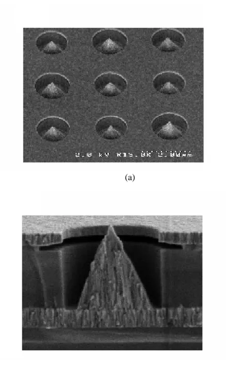
Figure 1-1 The SEM micrograph of (a) Spindt type triodes array, (b) Spindt type field emission triode
Figure 1-2 The schematic diagram of (a) conventional CRT, (b) FED.
Figure 1-3 Energy diagrams of vacuum-metal boundary: (a) without external electric field; (b) with an external electric field.
Figure 1-4 The FED products based on Spindt type field emitters, (a) motorola 5.6” color FED, (b) Pixtech 5.6” color FED, (c) Futaba 7” color FED and (d) Sony/Candescent 13.2” color FED.
Figure 1-5 (a) Si tip formed by isotropic etching and (b) Si tip field emission triodes array formed by CMP
Figure 1-6 (a) SEM image of SCE cathode array (b) structure of SED (c) a 36-inch prototype of surface conduction electron emitter display
Figure 1-7 High-resolution transmission electron microscopy images of (a) single-walled nanotubes (SWNTs) and (b) multiwalled nanotubes (MWNTs). Every layer in the image (fringe) corresponds to the edges of each cylinder in the nanotube assembly.
Figure 1-8 Molecular models of single-walled nanotubes with different helicities: (a) zig-zag arrangement; (b) armchair configuration; (c) and (d) two different helicities. Figure 1-9 (a) SEM image of CNT cathode from Samsung’s FED, (b) a 4.5-inch FED from
Samsung, the emitting image of fully sealed SWNT-FED at color mode with red, green, and blue phosphor columns, and (c) a prototype of 5” CNT flat panel display by Samsung
Chapter 2
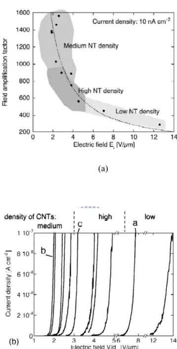
Figure 2-1 (a) Simulation of the equipotential lines of the electrostatic field for tubes of 1 μm height and 2 nm radius, for distances between tubes of 4, 1, and 0.5 μm; along with the corresponding changes of the field enhancement factor β and emitter density (b), and current density (c) as a function of the distance.
(Ref. Appl. Phys. Lett. 76 (2000) 2071)
Figure 2-2 (a) Field amplification factor β as a function of the onset field after training, Ei, for the films obtained by CVD with different catalyst concentrations. (b) Low current field emission characteristics of the 11 samples after training.
(Ref. Carbon 40 (2002) 1715)
Figure 2-3 Experimental procedures of patterned CNTs synthesized by thermal CVD.
Figure 2-4 (a) (b) Show photo and schematic pictures of thermal CVD, and (c) the growth condition of CNTs in the thermal CVD.
Figure 2-5 Schematic diagram of a high-vacuum system setup for field emission measurement.
Figure 2-6 The SEM images of CNTs with different thicknesses of the thin Ti capping layer from a 45° viewing angle: (a) 0 nm, (b) 0.5 nm, (c) 1 nm, (d) 2 nm, and (e) 4 nm. Figure 2-7 The SEM images of CNTs with different thicknesses of the thin Ti capping layer
from the top view: (a) 0 nm, (b) 0.5 nm, (c) 1 nm, (d) 2 nm, and (e) 4 nm.
Figure 2-8 The field emission properties: (a) the relationship between emission current density and electric field (b) the Fowler-Nordheim plot
Figure 2-9 Experimental procedures of patterned CNTs synthesized by thermal CVD.
Figure 2-10 The SEM images of pre-treated catalytic nanoparticles with different thicknesses of the thin Ti capping layer: (a) 0 nm, (b) 1 nm, (c) 2 nm, (d) 4 nm, (e) 10 nm, and (f) 20 nm.
from a 45° viewing angle: (a) 0 nm, (b) 1 nm, (c) 2 nm, (d) 4 nm, (e) 10 nm, and (f) 20 nm.
Figure 2-12 The SEM images of CNTs with different thicknesses of the thin Ti capping layer from the top view: (a) 0 nm, (b) 1 nm, (c) 2 nm, (d) 4 nm, (e) 10 nm, and (f) 20 nm.
Figure 2-13 The HRTEM images of CNTs with (a) (b) low magnification images, and (c) (d) high magnification images of sidewall and intertube, respectively.
Figure 2-14 The EDS analysis of the catalytic nanoparticle in CNTs
Figure 2-15 The field emission properties: (a) the relationship between emission current density and electric field (b) the Fowler-Nordheim plot
Figure 2-16 Experimental procedures of patterned CNTs synthesized by thermal CVD.
Figure 2-17 The SEM images of CNTs with different weight percentages of Ti from the top view: (a) 0 %, (b) 36 %, (c) 53 %, (d) 70 %, and (e) 85 %.
Figure 2-18 The SEM images of CNTs with different weight percentages of Ti from a 90° viewing angle: (a) 0 %, (b) 36 %, (c) 53 %, (d) 70 %, and (e) 85 %.
Figure 2-19 The HRTEM images of CNTs with (a) low magnification images and (b) high magnification images.
Figure 2-20 The EDS analysis of the catalytic nanoparticle in CNTs
Figure 2-21 The field emission properties: (a) the relationship between emission current density and electric field (b) the Fowler-Nordheim plot
Figure 2-22 The luminescent images on the ITO anode with phosphor coating on it were observed. Samples (a), (b), and (c) showed the Fe/Ti (5 nm/50 nm) film at applied electric field 5, 6, and 7 V/μm, respectively. Samples (d), (e), and (f) showed the Fe/Ti (5 nm/ 50 nm) film and a 2-nm-thick Ti capping layer was deposited after pre-treatment at applied electric field 5, 6, and 7 V/μm, respectively. Samples (g), (h), and (i) showed the weight percentage of Ti was 36
% in the co-deposition of Fe and Ti were deposited on the 50-nm-thick Ti buffer layer at applied electric field 5, 6, and 7 V/μm, respectively. The distance of spacer was 100 μm and these samples were square cells with length of 1 cm. Figure 2-23 (a) Lindemann Criterion
The primitive situation after deposition (b) and two synthetical mechanisms of CNTs growth (c) Fe catalytic nanoparticles might be revealed out (d) Fe catalytic nanoparticles might not be revealed out but the carbon radicals still could diffuse through the thin Ti film.
Chapter 3
Figure 3-1 (a) (b) The SED jointly developed by Canon and Toshiba Corporation and (c) (d) showed the field emission efficiency.
Figure 3-2 The traditional triode structure (oxide-poly) and the field emission efficiency. Figure 3-3 The simulations of (a) (b) Electrostatic potential and (c) (d) Electric field with
oxide-poly structure.
Figure 3-4 Experimental procedures of triode structure with oxide-poly composition.
Figure 3-5 (a) (b) Show photo and schematic pictures of thermal CVD, and (c) the growth condition of CNTs in the thermal CVD.
Figure 3-6 Fe/Ti (5 nm/50 nm) patterns were formed (a) before lift-off and (b) after lift-off. (c) (d) (e) Showed the structure of oxide-poly composition and the morphology of CNTs.
Figure 3-7 The field emission properties: (a) the relationship between emission gate current density and gate voltage (b) the relationship between emission anode current density and gate voltage and the inset showed the Fowler-Nordheim plot
Figure 3-8 The emission anode current density versus anode voltage with different gate bias. Figure 3-9 Experimental procedures of triode structure with oxide-nitride-poly composition.
Figure 3-10 Fe/Ti (5 nm/50 nm) patterns were formed (a) before lift-off and (b) after lift-off. (c) (d) (e) Showed the structure of oxide-nitride-poly composition and the morphology of CNTs.
Figure 3-11 The field emission properties: (a) the relationship between emission gate current density and gate voltage (b) the relationship between emission anode current density and gate voltage and the inset showed the Fowler-Nordheim plot
Figure 3-12 The emission anode current density versus anode voltage with different gate bias. Figure 3-13 The simulations of electrostatic potential with oxide-nitride-poly structure. Figure 3-14 Experimental procedures of triode structure with oxide-poly-nitride composition. Figure 3-15 Fe/Ti (5 nm/50 nm) patterns were formed (a) before lift-off and (b) after lift-off.
(c) (d) (e) Showed the structure of oxide-poly-nitride composition and the morphology of CNTs.
Figure 3-16 The field emission properties: (a) the relationship between emission gate current density and gate voltage (b) the relationship between emission anode current density and gate voltage and the inset showed the Fowler-Nordheim plot
Figure 3-17 The emission anode current density versus anode voltage with different gate bias. Figure 3-18 The simulations of electrostatic potential with oxide-poly-nitride structure.
Figure 3-19 The field emission properties: (a) the relationship between emission gate current density and gate electric field (b) the relationship between emission anode current density and gate electric field
Chapter 1
Introduction
1.1 Overview of Vacuum Microelectronics 1.1.1 History
Since the invention of solid state transistors in the late 1940s, vacuum tubes have been gradually replaced by those tiny volume, low cost, better reliability, and more power efficient solid state devices. With great improvements on semiconductor manufacturing technology for the past decades, the so called vacuum microelectronic devices using the professional micro fabrication technology have been successfully fabricated and gave a new life to vacuum electronics. “Vacuum state” devices have a number of remarkable advantages with respect to the present “solid state” devices, including fast carrier drift velocity, radiation hardness, and temperature insensitivity. For example, the saturation drift velocity is limited to less than 3×10⁷
cm/s in all semiconductor due to scattering mechanism whereas the saturation drift velocity in vacuum is limited theoretically to 3×1010 cm/s and practically to about 6-9×10⁸
cm/s [1.1]. Moreover, because there is no medium to be damaged, either temporarily or permanently radiation effect should be negligible in vacuum devices. Additionally, there is no medium for electrons fly in the vacuum, so there is no lattice scattering or bulk carrier generation/recombination. Therefore, the vacuum microelectronic devices can suffer to 500℃ or above as long as the structures of the vacuum devices do not destroyed [1.2]. Table 1-1 shows the comparison between vacuum microelectronic and semiconductor devices.
Recent development in vacuum microelectronics started in 1928, when R. H. Fowler and L. W. Nordheim published the first theory of electron field emission from metals using quantum mechanics [1.3]. This theory is contrary to thermionic emission, which metals have to be heated so that some of the electrons in metal gain enough thermal energy to overcome
the metal/vacuum barrier; according to the Fowler-Nordheim theory, an applied electric field of approximately 103 V/μm is needed for electrons to tunnel through the sufficiently narrow barrier [1.3]. To reach this high field at reasonable applied voltage, it is customary to machine the field emitters into protruding objects to take advantage of field enhancement. It was not until 1968 when C. A. Spindt camp up with a fabrication method to create very small dimension metal cones that vacuum microelectronic triodes became possible [1.2]. Figure 1-1 is a schematic diagram of the triode fabricated by Spindt. From the late 1960s to the year 1990, Ivor Brodie, Henry F. Gray, and C. A. Spindt made many contributions to this field. Also, most of research was focused on the devices similar to the Spindt cathode during the past three decades.
In 1991, a group of research of the French company LETI CHEN reported a microtip display at the fourth International Vacuum Microelectronics Conference [1.4]. Their display was the first announcement of a practical vacuum microelectronic device. From then on, a great amount of researchers all over the world devoted themselves to this interesting, challenging, and inventive field. Part of the work focused on fabricating very small radius silicon tip by utilizing modern VLSI technology [1.5-1.6]. Some of them increased the emission current by coating different metals, such as W, Mo, Ta, Pt etc., even diamond on field emission arrays [1.7-1.9]. Different device schemes also have been proposed to enhance the emission current density, stability, and reliability.
1.1.2 Applications of Vacuum Microelectronic Devices
Among wide range applications of the vacuum microelectronics, the first commercial product could be the field emission flat-panel display [1.10-1.14]. The field emission fluorescent display is basically a thin cathode ray tube (CRT), which was first proposed by SRI International and later demonstrated by LETI [1.4].
electroluminescent display (EL), vacuum fluorescent display (VFD), plasma display panel (PDP), and light emitting display (LED), are developed for the better characteristics of small volume, light weight, and low power consumption. LCDs have become the most popular flat panel displays, however, LCDs have some drawbacks, such as poor viewing angle, temperature sensitivity and low brightness. As a result, some opportunities still exist and waiting for the solutions from other flat panel displays such as FED.
1.1.3 Field Emission Displays
FED features all the pros of the CRTs in image quality and is flat and small volume. The schematic comparisons are revealed in Figure 1-2. The operation of CRTs involves deflection of the beam in such a way that the electron spot scans the screen line-by-line. In FEDs, multiple electron beams are generated from the field emission cathode and no scanning of beams is required. The cathode is a part of the panel substrate consists of an X-Y electrically addressable matrix of field emission arrays (FEAs). Each FEA is located at the intersection of a row and a column conductor, with the row conductor serving as the gate electrode and the column conductor as the emitter base. The locations where the rows and columns intersect define a pixel. The pixel area and number of tips are determined by the desired resolution and luminance of the display. Typically, each pixel contains an FEA of 4-5000 tips. The emission current required for a pixel varies from 0.1 to 10 μA, depending on the factors such as the luminance of the display, phosphor efficiency and the anode voltage. Compared to the active matrix LCDs, FEDs generate three times the brightness with wilder viewing angle at the same power level. Full color FEDs have been developed by various research groups from different aspects such as PixTech, Futaba, Fujitsu, Samsung, are presently engaged in commercially exploiting FED.
1.1.4 Theory Background
Electron field emission is a quantum mechanical tunneling phenomenon of electrons extracted from the conductive solid surface, such as a metal or a semiconductor, where the surface electric field is extremely high. If a sufficient electric field is applied on the emitter surface, electrons will be emitted through the surface potential barrier into vacuum, even under a very low temperature. In contrast, thermionic emission is the hot electron emission under high temperature and low electric field. Figure 1-3(a) demonstrates the band diagram of a metal-vacuum system.
Here W0 is the energy difference between an electron at rest outside the metal and an
electron at rest inside the metal, whereas Wf is the energy difference between the Fermi level
and the bottom of the conduction band. The work function φ is defined as φ = W0 - Wf. If an
external bias is applied, vacuum energy level is reduced and the potential barrier at the surface becomes thinner as shown in Figure 1-3(b). Then, an electron having energy “W” has a finite probability of passing through the surface barrier. Fowler and Nordheim derive the famous F-N equation (1.1) as follow [1.3]:
( )
exp[ 2 ( )/ ] 3 2 2 E y v b y t aE J φ φ − = , (1-1) where J is the current density (A/cm2). E is the applied electric field (V/cm), φ is the work function (in eV), a = 1.56×10⁻⁶, b = -6.831×10⁻⁷, y = 3.79x10-4×10-4E1/2/φ, t2(y)~1.1 and v(y) can be approximated as [1.15] ), 5 . 0 cos( ) (y y v = π (1-2) or . 95 . 0 ) (y y2 v = − (1-3) Typically, the field emission current I is measured as a function of the applied voltage V. Substituting relationships of J = I/α and E = βV into Eq.(1-1), where α is the emitting area and β is the local field enhancement factor at the emitting surface, the following equation can
be obtained ] ) ( exp[ ) ( 2 3 2 2 2 V y bv y t V A I β φ φ αβ − = . (1-4)
Then taking the log. form of Eq. (1-4) and v(y) ~ 1
) ) ( ( 10 97 . 2 ] ) ( 10 54 . 1 log[ ) log( 2 3 7 2 2 6 2 V y v y t V I β φ φ αβ − × × = − , (1-5)
from Eq. (1-5), the slope of a Fowler-Nordheim (F-N) plot is given by
) ( 10 97 . 2 2 3 7 β φ × − = ≡slopeFN S , (1-6) The parameter β can be evaluated from the slope S of the measured F-N plot if the work function φ was known
) ( 10 97 . 2 2 3 7 S φ β =− × (cm-1), (1-7)
The emission area α can be subsequently extracted from a rearrangement of Eq. (1-5)
) 10 53 . 6 exp( ) 89 . 9 exp( 10 4 . 1 ) ( 2 3 7 2 6 2 V V I β φ φ β φ α − × × = − (cm2). (1-8)
For example, the electric field at the surface of a spherical emitter of radius r concentric with a spherical anode (or gate) of radius r+d can be represented analytically by
) ( d d r r V E= + , (1-9) Though a realistic electric field in the emitter tip is more complicated than above equation, we can multiple Eq.(1-9) by a geometric factor β` to approximate the real condition.
≡ tip E function of (r,d) =β ` ( ) d d r r V + , (1-10) where r is the tip radius of emitter tip, d is the emitter-anode(gate) distance and β` is a geometric correction factor [1.16].
r>>d, Etip approaches to β`(V/d) which is the solution for a parallel-plate capacitor and for a
diode operation in a small anode-to-cathode spacing.
As the gated FEA with very sharp tip radius, Eq. (1-10) can be approximated as:
Etip =β`(V/r). (1-11)
Combining E = βV and Eq. (1-11), we can obtain the relationship:
Etip =βV =β`(V/r), and β`= βr. (1-12)
The tip radius r is usually in the range from a few nm to 50 nm, corresponding to the parameter β` ranging from 10-1 to 10-2.
Besides, transconductance of a field emission device is defined as the change in anode current due to a change in gate voltage [1.1].
m g g C m V I g ∂ ∂ = |Vc, (1-13)
Transconductance of a FED is a figure of merit that gives as an indication of the amount of current charge that can be accomplish by a given change in grid voltage. The transconductance can be increase by using multiple tips or by decreasing the gate-to-cathode spacing for a given anode-to-cathode spacing.
According to the above mention equations (especially Eq.1-5), the following approaches may therefore be taken to reduce the operating voltage of the field emission devices:
1) Find techniques to reproducibly sharpen the tips to the atomic level (increaseβ). 2) Lower the work function of the tip (φ).
3) Narrow the cone angle (increaseβ).
4) Reduce the gate-opening diameter (increaseβ).
1.2 Cathode Structures and Materials for Field Emission Displays
the drawbacks of TFT-LCD, such as poor viewing angle, temperature sensitivity and low brightness. However, some difficult technological subjects should be considered such as microfabrication of cathodes, assembly technology with accuracy of micrometer level, vacuum technology to keep stable field emission in small space of flat panels and high efficiency phosphor materials. This section introduces some novel cathode structures and synthesizes these novel emitter materials for FED operations.
1.2.1 Spindt-type Field Emitters
The “Spindt” cathode was first proposed by C. A. Spindt in 1968 [1.17]. Figure 1-1 demonstrated the scanning electron microscope (SEM) image of a spindt type field emission triode [1.18], which was invented by Spindt of SRI and improved for the electron source of high-speed switching devices or microwave devices [1.2]. Meyer of LETI presented the capability of using Spindt-type emitters for a display in 1970s [1.19] and stabilized the field emission from Spindt-type emitters by introducing a resistive layer as the feedback resistance.
This proposal triggered the development of field emitters as an electron source of displays by researchers and electronics makers in 1990. The merits of the Spindt type field emitters are summarized as following: (1) High emission current efficiency, more than 98% anode current to cathode current can be achieved for the symmetric structure of Spindt tip and the gate hole, the lateral electric field to the metal tip can be cancelled out. (2) The fabrication is self-aligned, easy process; uniform field emission arrays can be fabricated easily. Some research groups have successfully fabricated commercial FED products based on Spindt type field emitters such as motorola, Pixtech, Futaba and Sony/Candesent.[1.20], the products of above mentioned companies are shown in Figures 1-4.
However, there are some existing drawbacks of Spindt type field emitters when fabricating Spindt type FED such as (1) High gate driving voltage required; for a Spindt type field emission triode with 4 μm gate aperture, the driving voltage is typically more than 60 V,
which results in the high cost of the driving circuits. To reduce the gate driving voltage, frontier lithography technologies such as E beam lithography must be applied to reduce the gate aperture to the sub-micron level. (2) The emission property degrades for the chemically instable of the metal tips. (3) Huge, expensive high vacuum deposition system required during fabricating large area Spindt type FED.
1.2.2 Si Tip Field Emitters
An alternative approach to fabricate tip type field emitters is to fabricate the Si tip field emitters based on the semiconductor fabricating process. Figures 1-5 depict the SEM micrographs of Si tips array, Si tip field emission triodes array formed by chemical mechanical polishing (CMP) [1.21] and double gate of Si field emitter arrays [1.22]. Symmetric device structure and similar advantages with Spindt type field emitters can be obtained. However, high temperature oxidation sharpening process prohibits Si tip from large area fabrication.
1.2.3 Carbon and Nano-sized Emitters
Carbon nanotubes have attracted a great deal of interest owing to their advantageous properties, such as high aspect ratios, small tip radius of curvature, high Young’s modulus, capability for the storage of a large amount of hydrogen, and structural diversities that make it possible for band gap engineering. These useful properties of carbon nanotubes (CNTs) make themselves good candidates for various applications, for instance, wires for nanosized electronic devices, super strong cables, AFM tips, charge-storage devices in battery, and field emission display.
1.2.4 Surface Conduction Electron Emitter (SCE)
Toshiba. Like conventional CRTs, SEDs utilize the collision of electrons with a phosphor-coated screen to emit light. The key technology to the electron emitters begins with the creation of an extremely narrow slits (~ several nanometers) between two electric poles in thin film of PdO (Palladium Oxide). Electrons are emitted from one side of the slit when approximately 10 V of electricity are applied. Some of these electrons are scattered at the other side of the silt and accelerated by the voltage (approximately 10 kV) applied between the glass substrates; causing light to be emitted when they collide with the phosphor-coated glass plate. The PdO film is coated by inject printing or screen-printing technology and this is a low cost process. The major problem of SED is that the efficiency is still low and the power consumption will be very high. Figure 1-6 shows the SEM image of SCE cathode array, structure and a 36-inch display of SED [1.23-1.24].
1.3 Field Emission Properties of Carbon Nanotubes 1.3.1 Structure and Properties of Carbon Nanotubes
Recently, carbon nanotubes have attracted a lot of attention owing to their unique properties and potential for various applications. The discovery of nanotubes happened in 1991 when Sumio Iijima of NEC Corporation found these tiny needles, consisting of concentric graphite tubes, on the electrodes used to prepare fullerenes [1.25]. Nanotubes can be divided into two categories. The first is called multiwalled carbon nanotubes (MWNTs). MWNTs are close to hollow graphite fibers [1.26], except that they have a much higher degree of structural perfection. They are made of sheets of carbon atoms with a cylindrical shape and generally consist of co-axially arranged 2 to 20 cylinders「Figure 1-7(b)」. The interlayer spacing in MWNT (d(002) = 0.34 nm) is slightly larger than that in single crystal
graphite (d(002) = 0.335 nm) [1.27]. This is attributed to a combination of tubule curvature and
nanotube is made up of just a single layer of carbon atoms. These nanotubes are called the single-walled nanotubes (SWNTs) and possess good uniformity in diameter about 1.2 nm 「Figure 1-7(a)」. They are close to fullerenes in size and have a single-layer cylinder extending from end to end [1.28-1.29].
These unique structural properties are ascribed to the building material of nanotube---carbon. Carbon is the elemental equivalent of the perfect neighbor, friendly, and easygoing. Under intense pressure, carbon atoms form co-valence bonds with four neighbor atoms, creating the pyramidal arrangement of diamond. However, the activation energy of diamond is very high and carbon usually links up with just three neighbors, creating the hexagonal rings of graphite network. The arrangement of graphite has a host of unpaired electrons, which essentially float above or below the plane of carbon rings. In this arrangement, the electrons have more freedom to move around the graphite surface, which makes the material a good electrical conductor.
Carbon nanotubes consist of concentric hexagon-rich cylinders, made up of sp2 hybridized carbon, as in graphite, and terminated by end-caps arising from the presence of 12 pentagons (six per end). It is possible to construct a cylinder by rolling up a hexagonal graphene sheet in different ways. Two of these are “non-helical” in the sense that the graphite lattices at the top and bottom of the tube are parallel. These arrangements are named “armchair” and “zig-zag”. In the armchair structure, two C-C bonds on opposite sites of each hexagon are perpendicular to the tube axis, whereas in the zig-zag arrangement, these bonds are parallel to the tube axis 「Figure 1-8 (a)(b)」. In all other conformation, the C-C bonds lie at an angle to the tube axis and a helical structure is obtained 「Figure 1-8 (c)(d)」.
Theoretical calculations have predicted that all the armchair tubes are metallic whereas the zig-zag and helical tubes are either metallic or semiconducting [1.30-1.31]. The electronic conduction process in nanotubes is unique since in the radial direction, the electrons are confined in the singular plane of the graphene sheet. The conduction occurs in the armchair
(metallic) tubes through gapless modes as the valence and conduction bands cross each other at the Fermi energy. In most helical tubes, which contain large numbers of atoms in their unit cell, the one-dimensional band structure shows an opening of the gap at the Fermi energy, and this leads to semiconducting properties. This unique electronic behavior only occurs for small nanotubes. As the diameter of the tubes increases, the band gap (which varies inversely with the tube diameter) tends to zero, yielding a zero-gap semiconductor that is electronically equivalent to the planar graphene sheet. In a MWNT, the outer planar graphene-like tubes superimpose the electronic structure of the inner tubes. This has been proved by several experiments [1.32-1.33] where the band structure obtained from individual MWNT resembles that of graphite. Experiments have indicated that the pentagonal defects present at the tips can induce metallic character by introducing sharp resonance in the local density of states near the Fermi energy [1.33]. Similar metallization of nanotubes is also found to occur through the substitutional doping of the nanotube lattice with impurities such as boron and nitrogen [1.34].
1.3.2 Potential Applications of Carbon Nanotubes
Since the discovery of CNTs in 1991, they have been attracting much attention for their unique physical and chemical properties, such as high aspect ratio, low work function (5 ev), small tip radius of curvature, high chemical stability, high mechanical strength, high conductivity, and electron emission properties [1.35-1.36]. Therefore, one of the most potential application of carbon nanotubes is as the field emission material in vacuum microelectronics, such as flat-panel field-emission displays (FEDs), nanoprobes of atomic force microscopes (AFMs), microsensors, scanning tunneling microscopes (STMs) and microsized intense electron sources.
According to Fowler-Nodiem theory, the electric field at the apex of a needle-shaped tip is enhanced by a factor β = h/r, where h is the height of the tip and r is the radius of curvature
of the tip apex. The carbon nanotube is a stable form of carbon and can be synthesized by several techniques. They are typically made as threads about 10-100 nm in diameter with a high aspect ratio (>1000). These geometric properties, coupled with their high mechanical strength and chemical stability, make carbon nanotubes attractive as electron field emitters. Several groups have recently reported good electron field emission from nanotubes [1.37-1.39].
In 1999, Samsung pronounced a 4.5-inch carbon nanotube based field emission display (Figure 1-9(b)). They mixed a conglomeration of single-walled CNTs into a paste with a nitrocellulose binder and squeezed the concoction through a 20-μm mesh onto a series of metal strips mounted on a glass plate (Figure 1-9(a)). As the CNTs emerged from the mesh, they were forced into a vertical position. The metal strips with the CNTs sticking out of them served as the back of the display. The front of the display was a glass plate containing red, green, and blue phosphors and strips of a transparent indium-tin-oxide anode running from side to side. The glass plates were separated by spacers with the thickness of 200 μm. Once assembled, the edges were sealed and air was pumped out of the display.
Samsung’s 5-inch carbon nanotube based field emission display (Figure 1-9(c)) could be the precursor of a new generation of more energy efficient, high performance flat panel displays for portable computers [1.40]. The CNTs appear to be durable enough to provide the 10000-h lifetime considered being a minimum for an electronic product. The panel consumes just half the power of an LCD to generate an equivalent level of screen brightness. They could also be cheaper than LCDs or other types of field emission displays being developed. Until now, at last five major Japanese electronic manufactures are working on this technology.
1.4 Thesis Organization
theory and applications of carbon nanotubes are described.
In chapter 2, we reveal the synthesis of the carbon nanotubes and improve field emission characteristics of carbon nanotubes by a thin Ti capping layer or co-deposition process. These simple methods to produce the patterned carbon nanotubes using thermal CVD are introduced. Then, the capping layer process and co-deposition process are introduced to reduce the turn-on field and improve the emission current density. Moreover, the issues of reliability and uniformity of carbon nanotubes are discussed in this chapter.
In chapter 3, the triode structures acceded a nitride insulating layer are fabricated to reduce the gate leakage and improve the field emission efficiency. Because only a small fraction of electrons can pass through the gate holes and collected by the anode, we introduce these triode structures to change the distribution of electric field to draw more electrons toward the anode.
Finally, the conclusions and recommendations for future researches are provided in chapter 4.
Chapter 2
By Modification of Ti to Control the Density of CNTs and Improve the Field
Emission Properties
2.1 Motivation
As the field emission displays are going to be commercialized, it is very important to find a suitable cold cathode with low operating voltage and high emission current. According to the theory of field emission, Fowler-Nordheim tunneling, low work function (φ ), high field
enhancement factor (β), and large emission area (α) are desirable for a high field emission current density.
For the techniques of silicon tips, several methods have been used to obtain a large enhancement factor β via sharpening the silicon tips, such as large oblique-angle thermal evaporation or sputtering to fabricate sharp metal cones, high temperature oxidation to sharpen silicon tips, or anisotropic etching of silicon using KOH to produce sharp tip molds. However, these methods to fabricate sharp tips need extra fabrication process with complexity. The novel material, CNTs, therefore, is proposed to be one of the most promising materials as the cathodes in field emission displays.
The high density of CNTs can provide a great deal of field emission sites which can raise the emission current density (due to the increase of the emission area, α) but the density of CNTs will affect the field enhancement factor (β) which is also strongly relative to the emission properties of CNTs. For CNTs with high density, the screening effects reduce the field enhancement factor (β), therefore, suppress the field emission current density [2.1-2.3], as shown in Figure 2-1. Obviously, it is important to obtain an optimized density of CNTs to improve the field emission properties, such as turn-on field, threshold field, and emission current density. Well control of density and surface morphology of CNTs is thus required for
applications in the near future. To effectively control the density of CNTs, three novel methods including two thin Ti capping layer processes and a co-deposition of Ti and Fe process are introduced to improve the emission properties via controlling the density of CNTs in this chapter.
2.2 Introduction
Carbon nanotubes (CNTs) have attracted great deal of attention because of its outstanding physical properties and potential applications since its first observation by Iijima in 1991 [2.4]. Due to several unique properties, such as high aspect ratio, low work function (5 ev), small tip radius of curvature, high chemical stability, high mechanical strength, high conductivity, and electron emission properties [2.5-2.6], it has been considered as one of the most potential materials for field emission displays. Besides, CNTs is also a very wonderful materials in many applications, such as flat-panel field-emission displays (FEDs), nanoprobes of atomic force microscopes (AFMs), microsensors, scanning tunneling microscopes (STMs) and microsized intense electron sources. Nowadays, several methods have been developed to synthesize CNTs, such as arc discharge [2.7-2.8], laser ablation [2.9], screen-printing [2.10-2.12], plasma-enhanced CVD [2.13], electron cyclotron resonance CVD [2.14], microwave plasma-enhanced CVD [2.15], and thermal CVD [2.16-2.17]. Generally speaking, arc-produced CNTs, laser-produced CNTs, and screen-printing techniques are used to fabricate low-cost CNT field-emission in diode structure for field-emission displays. However, the drawbacks are that the specific purification processes for arc-produced and laser-produced CNTs are required, and the uniformity of screen-printed CNT field-emitter arrays is not applicable in filed emission displays. The selective growth of CNTs by chemical vapor deposition (CVD) processes without extra purification or screen-printing process, therefore, sufficient for fabricating field-emission devices with better uniformity. Besides, via the CVD
process, the CNTs can be grown with great vertical align which can also increase the effective local electric field when a voltage is applied. For these reasons, the thermal CVD, a simple, low cost, and well-developed method, is preferred to synthesize the CNTs in this thesis.
However, some critical issues such as screening effects, reliability, high driving voltage, uniformity, and vacuum package have not been solved for the application of field emission displays. The effect of screening electric field by the dense arrangement of CNTs has been reported by several groups [2.1-2.3]. If the CNTs are too closely spaced, the electric field will be screened out. Groning et al. reported the field enhancement factor β of the tips decreases rapidly when the inter-tip spacing is smaller than twice the length of the tips. They also found that the maximum current density is obtained when the spacing between the tips is about two times their relative height by simulations, as shown in Figure 2-1. For larger spacing the current density decreases due to the decreasing the field emission sites, with a nearly constant emission current per tip as the field enhancement factor remains constant. For smaller spacing the current density decreases rapidly due to the decreasing β factor and this effect cannot be compensated for by increasing the field emission sites from tips. This shows that when the spacing between the emitting structures on a surface becomes comparable to its length, problems of shielding do occur and will limit the emission current density.
Therefore, the turn-on field of the high-density-CNTs is still high because of the screening effects, as shown in Figure 2-2. To obtain better field emission properties, the density of CNTs should be optimized. However, the density of CNTs synthesized by thermal CVD is too high and the screening effects are very serious. Many researches have reported different methods to suppress this phenomenon, such as plasma treatment [2.18-2.21], wet etching method [2.22], screen-printing method used pastes with different CNT contents [2.23-2.24], E-beam lithography [2.25-2.26], anodic aluminum oxide (AAO) nanoporous templates [2.27-2.28], excimer laser irradiation [2.29], and etc.. Most of the methods will increase the complexity in processes of fabrication or cause a defective affection on the CNTs.
In this chapter, three novel processes including two kinds of thin Ti capping layer and a co-deposition of Ti and Fe process are proposed to modify the density of CNTs grown by thermal CVD. With different thicknesses of the Ti capping layer on hydrogen pretreated catalytic nanoparticles or different weight percentages of Ti co-deposited with catalyst, Fe, the density of CNTs can be controlled simply without the need of extra high cost or high complex processes. By controlling the density of CNTs, these methods can reduce the turn-on field and threshold field, and improve the field emission current density due to the suppressing of the screening effects. Furthermore, reliability is also a very important issue for field emission displays if it is going to be commercialized. The main factors to affect the lifetime of a CNTs-based emitter are the adhesion and the contact resistance between the CNTs and the substrate. With the novel methods proposed in this chapter, the adhesion can be increased to obtain a higher electric breakdown field and the contact resistance can also be suppressed to avoid the Joule heating when the devices are operated in a high current density condition [2.30-2.31].
2.3 Experiments
In this chapter, three novel methods including a thin Ti capping layer without pre-treatment, a thin Ti capping layer with pre-treatment, and co-deposited Fe with Ti, had been put forward to control the density of CNTs. Thereinafter, discussed about these three kinds of methods separately.
2.3.1 A Thin Ti Capping Layer without Pre-treatment 2.3.1.1 Experimental Procedures
The fabrication procedures of patterned CNT emitters were shown schematically in Figures 2-3(a) ~ 2-3(e). As shown in Figure 2-3(a), about 1-μm-thick photoresist was
spin-coated on an n-type silicon wafer (100) with low resistance and square cells with lengths of 10 μm, 100 μm, and 1000 μm were defined by photolithography. Then a Ti layer with 50-nm in thickness was deposited by the E-beam evaporation system as a buffer layer and a Fe layer with 5-nm in thickness was deposited subsequently as catalytic metal in the same system, as shown in Figure 2-3(b). The Fe/Ti (5 nm/50 nm) patterns were formed after the photoresist was removed by lift-off method as depicted in Figure 2-3(c). With different thicknesses (0, 0.5, 1, 2, and 4 nm) of a thin Ti capping layer was deposited in the sputtering system shown in Figure 2-3(d). Finally, CNTs were grown selectively by thermal CVD system to investigate the growth phenomenon and the field emission properties of CNTs that was shown in Figure 2-3(e). The samples with different Ti capping layers were loaded into the thermal CVD chamber (Figure 2-4(a) and (b)) to grow CNTs in atmospheric pressure at 700
with C
℃ 2H4 (5 sccm) for 10 min as depicted in Figure 2-4(c).
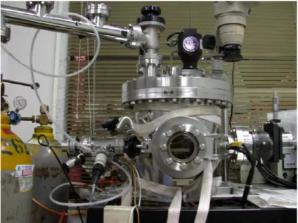
Scanning electron microscopy (SEM) was performed to discover the density and the morphology of CNTs. A high-vacuum measurement environment with a base pressure of 5x10⁻⁶ Torr was set up to characterize the field emission properties of CNTs (Figure 2-5). Cathode contact was made directly on the wafer. A glass plate coated with indium-tin-oxide (ITO) was positioned 120 μm to 160 μm above the sample surface as an anode. All cables were shielded except for the ground return path to the power source. The emission current densities of CNTs were measured as a function of applied electric field, using Keithley 237 high voltage units as DC source and Keithley 238 high current units as ground source. The measurement instruments were auto-controlled by the computer with IEEE 488 interface.
2.3.1.2 Results and Discussion
The corresponding thicknesses of the thin Ti capping layer were 0 nm, 0.5 nm, 1 nm, 2 nm, and 4 nm in SEM images from a 45° viewing angle as shown in Figures 2-6 (a), (b), (c), (d), and (e), respectively. From the SEM observation, the density of CNTs decreased if the
thickness of the thin Ti capping layer increased. As a speculation, the thin Ti capping layer could hinder the growth of CNTs as a diffusion barrier. With thicker Ti capping layer, the probability of carbon radicals to diffuse into the catalyst would be reduced therefore reduced the growth of CNTs. To estimate the density of CNTs, the SEM images were taken from top view and were shown in Figures 2-7 (a) ~ (e). To calculate the quantity conveniently, the pictures were divided into one fourth and then estimated the number of CNTs. Afterwards, the number which was multiplied by four was approximate density value. The approximate densities of CNTs could be counted and listed in Table 2-1(a). For the case of 0-nm-thick Ti capping layer, the density of CNTs was about 8.8x10⁸ emitter/cm2. With the increase of thickness of Ti capping layer, the density of CNTs was getting low. When the thickness of the thin Ti capping layer was increased to 4 nm, the density of CNTs had already dropped to 3x10⁶ emitter/cm2.
The field emission properties of CNTs with different thicknesses of the thin Ti capping layer were shown in Figure 2-8(a) which showed the relationship between emission current density and electric field (J-E). The corresponding Fowler-Nordheim plots for CNTs were depicted in Figure 2-8(b) and the linearity slope of the plots confirmed the field emission phenomena. From Table 2-1, the turn-on field defined at 10 μA/cm2 of CNTs decreased from 4.071 V/μm to 3.545 V/μm with the thickness of Ti capping layer was increased from 0 nm to 2 nm. From the SEM images, the density of CNTs also dropped from 8.8x10⁸ to 8x10⁶ emitter/cm2. This phenomenon may results from the suppression of the screening effects which can increase the field enhancement factor (β) hence reduce the turn-on field. However, the turn-on field did not always decrease with the increase in the thickness of the thin Ti capping layer. When the thickness of the thin Ti capping layer was added to 4 nm, the turn-on field would rise to 4 V/μm resulting from the decrease in the length of CNTs which would cause the reduction of aspect ratio and make the decline in the field enhancement factor (β).
electric field of 6 V/μm when the thickness of the thin Ti capping layer was from 0 nm to 2 nm, respectively. With a 4-nm Ti capping layer, the field emission current density dropped greatly as compared to the 2-nm one. It might result from the great reduction of emitting sites which could reduce the field emission current density effectively. With changing the thicknesses of the thin Ti capping layer from 0 nm to 4 nm, the field emission current density of CNTs was achieved to threshold field, which was defined at 10 mA/cm2, as the thickness of the thin Ti capping layer was 2 nm. Table 2-1(b) showed the summarized field emission properties of CNTs grown with different thicknesses of the thin Ti capping layer. The simulations of literature [2.23] predict that an inter-tube distance of about 2 times the height of CNTs optimizes the emitted current per unit area. In this experiment, the length of CNTs was probably 1 μm and this would correspond to an ideal density of 2.5x10⁷ emitter/cm2 by simulation. However, the optimum thin Ti capping layer thickness, 2 nm, was found out in this experiment and the density of CNTs of this sample was about 8x10⁶ emitter/cm2 which was similar to paper survey [2.23].
2.3.1.3 Summary
The density of CNTs could be controlled with different thicknesses of the thin Ti capping layer without pre-treatment and reduced the turn-on field and improved the field emission current density due to the suppression of screening effects. Low density could reduce the turn-on field, however, the number of the emitting sites would also be reduced hence cause the reduction in field emission current density. So it needed an optimized the thickness of the Ti capping layer to gain a reasonable field emission current density. In this experiment, the optimum thickness of thin Ti capping layer was found out to be 2 nm and the density of CNTs was altered from 8.8x10⁸ emitter/cm2 to 8x10⁶ emitter/cm2. The field emission current density was improved from 1.568 mA/cm2 to 10.2 mA/cm2 at the electric field of 6 V/μm and the turn-on field was decreased from 4.071 V/μm to 3.545 V/μm with the thickness of the Ti
capping layer increased from 0 nm to 2 nm. As a consequence, the experimental results revealed that the improvement of the field emission properties could be achieved by optimizing the density of CNTs with proper thin Ti capping layer thickness.
2.3.2 A Thin Ti Capping Layer with Pre-treatment 2.3.2.1 Experimental Procedures
The fabrication procedures of patterned CNT emitters were shown schematically in Figures 2-9(a) ~ 2-9(f). As shown in Figure 2-9(a), about 1-μm-thick photoresist was spin-coated on an n-type silicon wafer (100) with low resistance and square cells with lengths of 10 μm, 100 μm, and 1000 μm were defined by photolithography. Then a Ti layer with 50-nm in thickness was deposited by the E-beam evaporation system as a buffer layer and a Fe layer with 5-nm in thickness was deposited subsequently as catalytic metal in the same system, as shown in Figure 2-9(b). The Fe/Ti (5 nm/50 nm) patterns were formed after the photoresist was removed by lift-off method as depicted in Figure 2-9(c). Afterward the sample was pre-treated in the thermal CVD chamber in atmospheric pressure at 700 with ℃ H2 (500
sccm) and CH4 (200 sccm) for 5 min to form catalytic Fe nanoparticles as depicted in Figure
2-9(d). With different thicknesses (0, 1, 2, 4, 10, and 20 nm) of a thin Ti capping layer was deposited in the sputtering system shown in Figure 2-9(e). Finally, CNTs were grown selectively by thermal CVD system to investigate the growth phenomenon and the field emission properties of CNTs that was shown in Figure 2-9(f). The samples with different Ti capping layers were loaded into the thermal CVD chamber (Figure 2-4(a) and (b)) to grow CNTs in atmospheric pressure at 700 with C℃ 2H4 (5 sccm) for 10 min as depicted in Figure
2-4(c).
Scanning electron microscopy (SEM) was performed to discover the density and the morphology of CNTs. The wall structure and crystallinity of CNTs were determined by
high-resolution transmission electron microscopy (HRTEM) and the components of nanoparticles were analyzed by energy dispersive spectroscopy (EDS). A high-vacuum measurement environment with a base pressure of 5x10⁻⁶ Torr was set up to characterize the field emission properties of CNTs (Figure 2-5). Cathode contact was made directly on the wafer. A glass plate coated with indium-tin-oxide (ITO) was positioned 120 μm to 160 μm above the sample surface as an anode. All cables were shielded except for the ground return path to the power source. The emission current densities of CNTs were measured as a function of applied electric field, using Keithley 237 high voltage units as DC source and Keithley 238 high current units as ground source. The measurement instruments were auto-controlled by the computer with IEEE 488 interface.
2.3.2.2 Results and Discussion
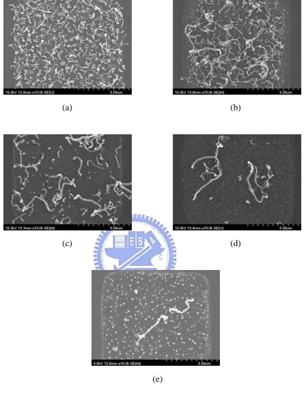
The SEM images of pre-treated Fe catalytic nanoparticles with different thicknesses of the thin Ti capping layer were shown in Figure 2-10. The thin Ti capping layer with 0 nm, 1 nm, 2 nm, 4 nm, 10 nm, 20 nm were corresponded to Figures 2-10(a), (b), (c), (d), (e), and (f), respectively. Figure 2-10(a) showed that the diameters of catalytic nanoparticles after pre-treatment were distributed randomly. With a 1-nm-thick Ti capping layer deposited after pre-treatment, some catalytic nanoparticles with small diameters were buried under the thin Ti capping layer, as shown in Figure 2-10(b). Form Figure 2-10(c), when the thickness of thin Ti capping layer was added to 2 nm, this phenomenon was come out to be more obvious due to more catalytic nanoparticles were buried under the increased Ti capping layer. Therefore, only some of catalytic nanoparticles with large diameters were remained as depicted in Figure 2-10(d). As the thickness of the Ti capping layer was increased to 10 nm or 20 nm, the samples in SEM images had only rough surfaces but obvious nanoparticles as displayed in Figures 2-10(e) and (f). Afterward, the samples with different thicknesses of Ti capping layers were loaded into the thermal CVD chamber to grow CNTs. The SEM images in Figure 2-11
showed the morphologies of subsequently grown CNTs. The corresponding thicknesses of the thin Ti capping layer were 0 nm, 1 nm, 2 nm, 4 nm, 10 nm, and 20 nm in SEM images from a 45° viewing angle as shown in Figures 2-11 (a), (b), (c), (d), (e), and (f), respectively. From the SEM observation, the density of CNTs decreased if the thickness of the thin Ti capping layer increased. It could be found that the thin Ti capping layer could hinder the growth of CNTs and the thickness of the thin Ti capping layer could be modified to control the density of CNTs. To estimate for the density of CNTs, the SEM images from the top view were taken in Figures 2-12 (a) ~ (f) corresponded to Figures 2-11 (a) ~ (f). To calculate the quantity conveniently, the pictures were divided into one fourth and then estimated the number of CNTs. Afterwards, the number which was multiplied by four was approximate density value. The approximate densities of CNTs were counted and listed in Table 2-2(a). For the sample without the Ti capping layer, the density of CNTs was about 2.8x10⁸ emitter/cm2. When the thickness of the thin Ti capping layer was increased to 20 nm, the density of CNTs had already dropped to much less than 1x10⁶ emitter/cm2.
In order to investigate the microstructure of CNTs, the high resolution transmission microscope (HRTEM) images were taken in Figure 2-13. The HRTEM images of CNTs with low magnification were shown in Figures 2-13(a) and (b). A nanoparticle was enclosed in the CNTs as shown in Figure 2-13(a). From the HRTEM images with high magnification in Figures 2-13(c) and (d), the layer-by-layer structure of graphite could be clearly observed. It could also demonstrate that the CNT in this TEM image was a multi-wall structure. Moreover, the composition of the catalytic nanoparticle was analyzed by energy dispersive spectrum (EDS) via the TEM instrument. The EDS spectrum in Figure 2-14 showed that only Fe, C, and Cu existed in the results of the EDS analysis. The peaks of Cu were from the Cu mesh which was used to hold CNTs in the TEM system. The peak of C was from the CNT and the peaks of Fe were from the catalytic nanoparticle enclosed in the CNT. No signal of Ti was detected which indicated that the Fe would not form the alloy with Ti in this process. From
the images of HRTEM and the analysis of EDS, Fe played a critical role in the growth of CNTs and Ti seemed not involve in the formation of CNTs by Ti-Fe alloy.
The field emission properties of CNTs with different thicknesses of the thin Ti capping layer were shown in Figure 2-15(a) which showed the relationship between the emission current density and the electric field (J-E). The corresponding Fowler-Nordheim plots for CNTs were also depicted in Figure 2-15(b) and the negative slope confirmed the Fowler-Nordheim tunneling phenomena. The turn-on field defined at 10 μA/cm2 of CNTs decreased from 3.786 V/μm to 2.107 V/μm with the thickness of the Ti capping layer increased from 0 nm to 4 nm. It might result from the suppression of the screening effects with the density of CNTs dropped from 2.8x10⁸ emitter/cm2 to 1.2x10⁷ emitter/cm2. However, the turn-on field did not always decrease with the increase in the thickness of the thin Ti capping layer. When the thickness of the Ti capping layer was added to 10 nm, the turn-on field would rise to 3.85 V/μm. It might due to the decrease in the length of CNTs which would result in the reduction of aspect ratio and cause the decline in the field enhancement factor (β). When the thickness of the Ti capping layer was added to 20 nm, there was almost no CNT could be observed via the SEM images due to the thickness of the Ti capping layer was too thick for carbon radicals to diffuse into the catalytic nanoparticles. The threshold field defined at 10 mA/cm2 of CNTs field emission diode decreased from 5.857 V/μm to 3.5 V/μm with the thickness of the thin Ti capping layer increased from 0 nm to 2 nm. The density of CNTs was decreased from 2.8x10⁸ emitter/cm2 to 2.8x10⁷ emitter/cm2. Here, the rise of the threshold field when the thickness of the thin Ti capping layer was 4 nm might due to the reduction of field emission sites.
The field emission current density was improved from 11.12 mA/cm2 to 97.6 mA/cm2 at electric field of 6 V/μm when the thickness of the thin Ti capping layer was increased from 0 nm to 2 nm, respectively. When the thickness of the thin Ti capping layer was 4 nm, the field emission current density dropped to 20.48 mA/cm2 at 6 V/μm because of the reduction of
field emission sites. Moreover, if the thickness of the thin Ti capping layer was over 2 nm, the field emission current density reduced with the increase of thickness and the field emission current density was almost zero when the thickness of the Ti capping layer was 20 nm. Table 2-2(b) showed the summarized field emission properties of CNTs grown with different thicknesses of the thin Ti capping layer. The simulations of literature [2.23] predict that an inter-tube distance of about 2 times the height of CNTs optimizes the emitted current per unit area. In this experiment, the average length of CNTs was probably 1 μm and this would correspond to an ideal density of 2.5x10⁷ emitter/cm2 by simulation. From the experimental results, the optimum thin Ti capping layer thickness, 2 nm, was found out in this experiment and the density of CNTs of this sample was about 2.8x10⁷ emitter/cm2 which was similar to the simulation results in the literature [2.23].
2.3.2.3 Summary
The density of CNTs could be controlled by a deposition with different thicknesses of the thin Ti capping layer on pretreated catalytic nanoparticles therefore reduced the turn-on field and improved the field emission current density. It might due to the suppression of screening effect. In this experiment, the optimum thin Ti capping layer thickness, 2 nm, was found out and the field emission current density improved from 11.12 mA/cm2 to 97.6 mA/cm2 at the electric field of 6 V/μm, the turn-on field decreased from 3.786 V/μm to 2.5 V/μm, and the density of CNTs was about 2.8x10⁷ emitter/cm2 which was similar to simulations for suppression the phenomenon of screening effect. As a consequence, the experimental results revealed that improved the field emission properties can be achieved by optimizing the density of CNTs under proper thin Ti capping layer thickness.