行政院國家科學委員會專題研究計畫 成果報告
創新異質整合智慧型手機相機模組之研究--子計畫一:微
機電防手振平台之設計、製作與測試(3/3)
研究成果報告(完整版)
計 畫 類 別 : 整合型 計 畫 編 號 : NSC 99-2220-E-009-002- 執 行 期 間 : 99 年 08 月 01 日至 100 年 07 月 31 日 執 行 單 位 : 國立交通大學電機與控制工程學系(所) 計 畫 主 持 人 : 邱俊誠 報 告 附 件 : 出席國際會議研究心得報告及發表論文 公 開 資 訊 : 本計畫可公開查詢中 華 民 國 100 年 10 月 31 日
中文摘要: 本計畫使用 SOI 製程技術設計並製作了兩種雙軸解耦合平台, 其中靜電式雙軸平台的尺寸為 12 x 12 x 0.5 mm3 而熱電式雙軸 平台的部份則為 8 x 8 x 0.2 mm3,當雙軸平台元件在進行影像 防手振功能時,兩種設計的結構強度均可承載影像感測器本身 的重量以進行 PDA 或是手機執行影像擷取時的防手振功能。製 作元件所使用的 SOI 製程包括了定義結構圖案之 ICP 蝕刻製 程,當元件製作完成後,使用覆晶封裝技術將市售的影像感測 晶片與雙軸平台結合以完成防手振模組的製作,為了要補償使 用手機相機模組照相時產生的手振,雙軸平台最大必須能夠在 各個方向制動 25um 的距離;在靜電式防振平台方面,為了避 免制動時所產生的側向位移使元件產生邊拉效應而使的電極短 路並損壞,本計畫設計了一種保護結構防止過大的側向位移, 而在熱電式防振平台的部分雖然不會有邊拉效應的產升,但是 側向位移仍會使平台產生非線性度影響,因此本計畫在熱電式 平台的設計中同樣的使用解耦合樑,並加入絕緣結構 SU8 以避 免制動時所產生的熱流回流使的熱殘留造成系統非線性與延遲 的情況產生。 英文摘要:
行政院國家科學委員會補助專題研究計畫
;
成 果 報 告
□期中進度報告
題目:
創新異質整合智慧型手機相機模組之研究
子計畫一:微機電防手振平台之設計、製作與測試
The design, fabrication and test of MEMS image stabilizer
計畫類別:□ 個別型計畫
;
整合型計畫
計畫編號:NSC 99-2220-E-009-044
執行期間:
99
年
08 月 01 日至
100
年
07 月 31 日
計畫主持人:
邱俊誠
共同主持人:無
計畫參與人員:林君穎
成果報告類型(依經費核定清單規定繳交):□精簡報告
;
完整報告
本成果報告包括以下應繳交之附件:
□赴國外出差或研習心得報告一份
□赴大陸地區出差或研習心得報告一份
□出席國際學術會議心得報告及發表之論文各一份
□國際合作研究計畫國外研究報告書一份
處理方式:除產學合作研究計畫、提升產業技術及人才培育研究計畫、列
管計畫及下列情形者外,得立即公開查詢
□涉及專利或其他智慧財產權,□一年□二年後可公開查詢
執行單位:
國立交通大學電機與控制工程學系
中 華 民 國 一百 年 五 月 卅一 日
行政院國家科學委員會專題研究計畫年度報告
題目: 創新異質整合智慧型手機相機模組之研究
子計畫一:微機電防手振平台之設計、製作與測試
“The design, fabrication and test of MEMS image stabilizer”
計畫編號:NSC 99-2220-E-009-044 執行期限:99 年 8 月 1 日至 100 年 7 月 31 日 主 持 人:邱俊誠 參與人員:林君穎
一、 摘要
本計畫使用 SOI 製程技術設計並製作了 兩種雙軸解耦合平台,其中靜電式雙軸平台的 尺寸為12 x 12 x 0.5 mm3 而熱電式雙軸平台 的部份則為8 x 8 x 0.2 mm3,當雙軸平台元件 在進行影像防手振功能時,兩種設計的結構強 度 均 可 承 載 影 像 感 測 器 本 身 的 重 量 以 進 行 PDA 或是手機執行影像擷取時的防手振功 能。製作元件所使用的SOI 製程包括了定義結 構圖案之ICP 蝕刻製程,當元件製作完成後, 使用覆晶封裝技術將市售的影像感測晶片與 雙軸平台結合以完成防手振模組的製作,為了 要 補 償 使 用 手 機 相 機 模 組 照 相 時 產 生 的 手 振,雙軸平台最大必須能夠在各個方向制動 25um 的距離;在靜電式防振平台方面,為了 避免制動時所產生的側向位移使元件產生邊 拉效應而使的電極短路並損壞,本計畫設計了 一種保護結構防止過大的側向位移,而在熱電 式防振平台的部分雖然不會有邊拉效應的產 升,但是側向位移仍會使平台產生非線性度影 響,因此本計畫在熱電式平台的設計中同樣的 使用解耦合樑,並加入絕緣結構 SU8 以避免 制動時所產生的熱流回流使的熱殘留造成系 統非線性與延遲的情況產生。 關鍵字: 雙軸平台、梳狀制動器、熱電式制 動器、影像防振Abstract
This project present two types 2-D decoupling XY stage, which are fabricated by using SOI wafer. The stages are 12 x 12 x 0.5 mm3 of electrostatic actuating XY stage and 8 x 8 x 0.2 mm3 of thermal actuating XY stage in size, and two structures are strong enough to suspend an image sensor as an image stabilizer applied in anti-shake photographic function. The stages can be used in a PDA or cell phone as an anti-shaking device when a picture is being taken. The image stabilizer is fabricated by the SOI process includes ICP etching process, which identify the structure layer. When the actuator is implemented, flip-chip bonding is adopted to attach the image sensor onto the decoupling XY stage. The XY stage is designed as image stabilizer to be installed in a cell phone. The longest calculated distance of motion of the stabilizer is designed to be 25um and a special stopper is also designed to prevent the actuator
from moving too far, sticking with pull-in phenomenon and circuit shorting of electrostatic actuating XY stage. Thought pull-in phenomenon will not happen in thermal actuating XY stage, the coupling movements induce the nonlinear effect to thermal actuator, to avoid the coupling movement and heat conductive problems, the decoupling structure and insulator SU8 are designed in thermal actuating XY stage.
Key words: XY stage, electrostatic, comb drive, thermal actuator, SOI process
二、 計畫緣由與目的
The MEMS-based XY stage can be realized by using micro fabrication processes due to advances in device miniaturization and high precision systems [1]. There are several actuator types of MEMS-based XY stage are used to drive the stage, one of main types is the electrostatic actuator, which usually be used in optical applications [2-7] and probe position systems [8] because it has good controllability and low power consumption, the applications of electrostatic XY stage include SPM (Scanning Probe Microscopy) probe [9,10], data storage [11-13], and nano-position control [1,14-16] .
However, electrostatic actuators usually require high driving voltage, for this reason, the step-up circuit must be designed very large, to decrease driving voltage, circuit size and increase actuating force, thermal actuators are researched and designed to generate larger actuating displacement [26].
The camera function has a growing role in cell phone applications. In addition to meeting the consumer demand for increased pixels,
digital single lens reflex (DSLR) camera functions are now being embedded in commercial cell phones. Anti-shake technology is among the many new technologies developed for mobile phones. The increasing number of camera pixels exacerbates the problem of image blurring caused by hand shaking. Image stabilization is the typical solution to this problem [17]. Among the familiar elements of image stabilization include lens shifting, [18] CCD shifting, [19] and signal processing [20]. The conventional anti-shaking technique in DSLRs, signal processing, is now used in mobile phones. Although signal processing requires no additional hardware and does not affect miniaturization of the system module, performance and reliability depend on the algorithm used. Given the demand for device miniaturization, the lens shifting anti-shaking approach is inadequate since adding a movable lens causes nonlinearity in control that must be compensated for by a complex control algorithm which must be corrected by a complex control algorithm. Although it requires an actuating system, IS shifting is less disruptive of miniaturization; the overall size of the system is also easier to reduce compared to lens shifting method. [17] The MEMS device enables suspended microstructures to be moved precisely and integrated with microelectronic circuits monolithically on a chip. [21] For the above reasons, a satisfactory image stabilizer design is needed to miniaturize cell phone camera modules.
A MEMS-based 2-dimensional decoupling thermal actuating XY stage is describe in this paper, which is designed and fabricated to reduce driving voltage and chip size. The
designs of the image stabilizer are suitable for a cell phone equipped with a 3x optical zoom, an actuator that can move at least 25μm, [17] and a sufficiently strong structure to withstand a 3.5 × 3.5 × 0.1 mm3 IS load, from which it must be decoupled in two dimensions when driven. Therefore, the proposed design has a high aspect ratio and 50μm-thick silicon springs. Four decoupling springs for the main suspended and decoupling structures connect with the shuttle. The device is manufactured by an anti-isotropic etching process that includes double-side lithography, two ICP etching processes, and flip-chip bonding process. Regarding the electrical connection of the IS, the output routing includes 24 signal outputs from 8 signal springs. The required 25um displacement is achieved when driven in a moving direction with 20 DC voltages, and the decoupling effect in the opposite direction is excellent.
三、 研究方法及成果
3.1 Principle and structure Design 3.1.1 Electrostatic actuating XY stage
The XY stage designed herein is driven by electrostatic force. Figure 1 shows a simple schematic diagram of the Comb-Driven model. When a potential difference is applied between fixed and movable comb fingers, an electrostatic force is generated, causing the relative displacement of the movable comb fingers (Figure.1). The driving force is F, can be expressed as d V nt d F o r 2 2 1 U = ∈ ∈ ∂ ∂ = (1)
Where U is the energy associated with the
applied electric potential V; d is the gap between the fixed and movable comb fingers; t is the thickness of the electrodes, n is the number of pairs of comb fingers; ∈r is the relative permittivity of the dielectric material between the comb fingers, and ∈ is the permittivity in o air. For simplicity, the XY stage is considered to follow Hooke’s law. The relationship between displacement and the reaction force Fs in the x direction can be expressed as,
x k
Fs= x−system (2)
where kx-system is the equivalent spring stiffness
of the system in the X direction and x is the displacement caused by the electrostatic force. Equation (3) is the sum of Eqs.(1) and (2) and specifies the relationship between displacement x and driving voltage V.
system x r o dk V nt x − ∈ ∈ = 2 2 1 (3)
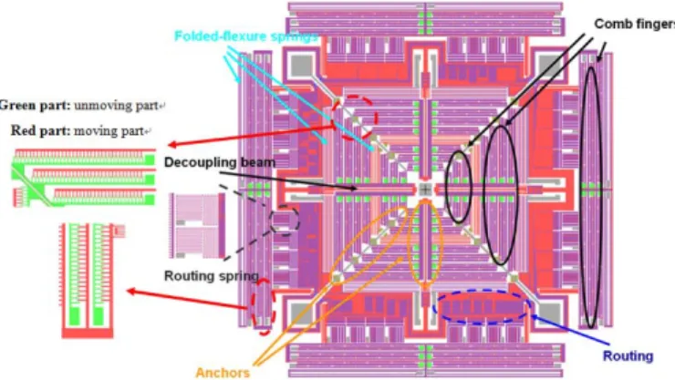
Figure 2 Schematic illustration of the XY stage. Table 1. Specifications of the image stabilizer.
Figure 2 shows the schematic illustration of electrostatic actuating XY stage, the design include decoupling beams, signal output beams and comb fingers, and the specifications of the electrostatic stage are shown in table 1.
3.1.2 Thermal actuating XY stage
Figure 3 shows a simple schematic diagram of the electro-thermal chevron actuator of the proposed image stabilizer.
Figure 3 Force acting on the chevron thermal actuator.
Applying voltage to pads generates an electro-thermal mechanical force, which changes the relative displacement between the XY stage and pads. When estimating driving displacement, several boundary conditions are assumed: 1. the actuator is heated uniformly, 2. pad temperatures are fixed at 300K, and 3. the expansion coefficient is a constant equal to Si expansion coefficient, 2.5 ppm/K. Under these conditions, the driving displacement is linearly related to temperature. Driving displacement can also be predicted by the equations below [27]:
2 2 A o / 2 y EI M M Fy F x x ∂ = = − − ∂ (4) where boundary conditions are:
0 |x 0 y = = ; y|x 0 y|x L/ 2 tan A x x δ δ θ δ = =δ = = ; ) ( EWT FL L L E E T× × = Δ + Δ = α σ (5)
where EI is the flexural rigidity, F is the reaction force along x-axis used to model the effects of thermal stress, Fo is the output force.
In Figure 3, L, W and T are the length, width and thickness of the actuator, respectively. The ΔT is the temperature change, ΔL is the change in L due to F, and α is the thermal expansion coefficient. Peak deflection is obtained by setting output force to zero, and peak output force is obtained by setting deflection to zero. The relationship between the lateral force for peak deflection and peak output force can be derived as follows:
max 2 maxtan
o A
The equation also gives peak output force according to peak deflection. The output force and displacement can be calculated by modifying actuator beam dimensions and gradients.
Figure 4 Illustrations of (a) chevron thermal actuator beams, (b) decoupling beams and (c) folded flexure beams.
Figure 5 Illustration of folded-flexure spring.
Figure 4 shows the three flexure beams used in this work. Figure 4(a) is a chevron thermal actuator. Since the pre-bending angle is very small, it can be simplified as three clamped-clamped beams parallel with each other [10]. Figure 4(b) shows a decoupling beam, according to the reference [28], the decoupling ratio must be larger than 10 when the pixel size and the maximum actuating displacement are 2.5μm and 25μm. Figure 4(c) is an IS signal output beam. Figure 5 shows the spring design of the structure [11] and the flexure beam specifications are shown below:
TABLE 2. Flexure Beam Specifications Spring type Fig. 4(a) Fig. 4 (b) Fig. 4 (c)
Length La1:630μm La2:300μm L:2000μm La1:900μm La2:790μm Width 30μm 20μm 25μm Height 50μm 50μm 50μm The proposed image stabilizer is designed to have an excellent decoupling effect and suitable device size for suspending the IS. The anti-shaking function is provided by a decoupling structure that compensates for hand shaking motion without an additional moving deviation in another direction. Figure 6(a) shows a simple schematic diagram of the proposed decoupling main structure. When a single direction force Fx is added to the decoupling structure, only a displacement △x parallel to
the driving force occurs and displacement in the opposite direction is negligible. Figure 6(b) illustrates a simplified operating mechanism of the proposed decoupling XY stage when different forces are applied in x- and y-directions. According to the decoupling design, the displacements in x- and y-directions are △x and
△ y, respectively, and mechanical isolation
between the two orthogonal driving directions is assumedly perfect.
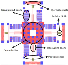
To suspend the IS, the actuator is designed and fabricated with a device thickness of 50μm, which provides sufficient stiffness in z-direction. For the signal outputs, circuit routing must be patterned upon the device layer. The signal routing springs and pads must be designed to maintain a working electrical connection. By flip-chip bonding and wire bonding, the routing springs and intermediary pad design make an electrical connection with cell phone circuits
from the IS pads to the electrical routing pads in the device structure and from the electrical routing pads in the device structure to the output PCB pads. Figure 7 schematically depicts the entire device design. According to the kinematic design shown in Figure 1, a main decoupling beam is designed separately in each direction to satisfy decoupling requirements. Each thermal-driven actuator has a push-only design, and each operates in only direction, i.e., X+, X-, Y+, or Y-. For the symmetrical springs design, the electrical routings have a balanced layout as well as two signal output springs and pads in each direction. The signal output springs are designed to be as thin as possible so that stiffness does not affect the overall spring constant system. Because of the isolation layers and the isolator SU-8, each electric potential between the structure and the signal output is independent.
(a) (b)
Figure 6 Illustration of driving modes of decoupling XY stage: (a) in X-direction only and (b) in both X- and Y-directions.
Figure 7 Structure design of XY stage.
3.2 Design and calculation of stage movement Most commercial cell phones have a 200 mega pixel or 300 mega pixels camera but no anti-shake function. People are always moving and are unable to picture without moving. Any vibration during the taking of a picture causes blurring. Figure 5 displays relationship between blurring pixel number and the angle of hand shaking. When the camera moves through an angle dθ in the horizontal plane, the blur pixel number can be represented as:
H L P d BP θ θ = (7) Where θL is the horizontal angle and PH
denotes the total horizontal pixel number. Typical low-cost camera systems have an angular field of view of 35º to 45º. For a 300 mega pixels image sensor with a field of view of 45º, experimental data [25] indicate that a 0.08º horizontal drift occurs in 2s of hand shaking, as recorded by an IDG-1000, a dual-axis gyroscope from InvenSense [25]. In this project, image sensor Micron MT9T012 with 3 mega pixels (2056x1544) is employed as the image sensor that is bonded on the designed device.
From Eq. (7), each pixel corresponds to a horizontal angle of 0.022º. Therefore, the number of horizontal blur pixels is approximately) 3.7. Since each pixel of MT9T012 has a size of 2.2x2.2μm2, the XY stage must have a range of motion of at least 8.14μm to enable the blur image to be adjusted. Given that many commercial cameras have x3 zoom-in and zoom-out functions, the range of motion must be three times this value, or 24.42μm.
Figure 8 Relation between blur pixel and angle.
3.3 Fabrication
The fabrication steps are device layer formation, substrate formation, and the final combination of IS and XY stage. Figure 9 depicts the device layer fabrication process. The steps required for device layer formation, including structure definition, heat isolation SU8, circuit routing and electric characterization isolation are completed in this segment. Fabrication begins with a (100) SOI wafer, where the thicknesses of the device layer, isolator and substrate are 50μm, 2μm and 350μm, respectively. Thus the entire fabrication process involves the following steps: a. After basic RCA cleaning, use CVD process to deposit a 0.5μm-thick layer of nitride and a 2μm-thick layer of silicon oxide on the device layer and substrate of the SOI wafer (Figure 9(a)).
b. During photolithography, pattern the nitride as the electric isolation between shuttle and circuit and signal output on the device side of the SOI wafer. (Figure 9(b));
c. Deposit a 1μm-thick layer of Al on the device layer by DC sputter and patterned as the circuits and pads. (Figure 9(c)).
d. Pattern the device layer by the first ICP process to a depth of 50μm (Figure 9(d)). e. Coat and pattern the SU8 in the heat and
electric isolation between the actuators and the XY stage. (Figure 9(e)).
f. Pattern the oxide layer on the substrate deposited in Figure 9(a) by using RIE as the hard mask of substrate etching process (Figure 9(f));
g. Perform the second ICP etching process is to open the suspending area on the backside of SOI wafer to a depth of 350μm (Figure 9(g)); h. Release the structure by RIE etching process
(Figure 9 (h)).
Figure 9 Fabrication process for the XY stage: (a)backside oxide deposition(2μm), (b)Nitride pattern(0.5μm), (c)Al pattern(1μm), (d)device layer pattern, (e)SU8 pattern, (f)backside oxide pattern, (g)backside layer pattern, (h)release.
3.4 Flip-chip bonding
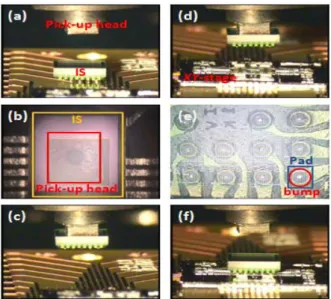
An IS is combined with the proposed image stabilizer by flip-chip approach. Figure 10 depicts the package process captured from the
flip-chip bonder monitor. Figure 10(a)-(c) show the IS absorbing process. Before absorption, the spectroscope is used to align the pick-up head and sensor (Figure 10(b)). Figures 10(d)-(f) show how the combination processes of the XY stage and IS align sensor bumps and pads of XY stage. Figures 10(e) and 10(f) show 3N force is applied to the IS then to reflow the bumps to 235 ° C, and figure 11 shows the reflow profile.
Figure 10 Flip-chip bonding process of the image stabilizer.
Figure 11 Reflow profile of flip-chip process
四、 量測結果
4.1 Electrostatic actuating XY stage
The effectiveness of the 2-D decoupled image stabilizer was assessed. During the static driving
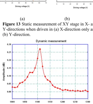
test, the actuator was driven by DC voltage. Actuator displacement was measured by a White Light Interferometer (WYKO) (Fig. 12). When a 51V driving voltage was applied to the proposed device in the x-direction, moving displacement in the x-direction was 25μm and displacement along the vertical y-axis was only 0.42μm. When a 54V driving voltage was applied to the proposed device in the y-direction, moving displacement in the y direction was 25μm and displacement along the vertical x-axis was only 0.34μm. In the x-direction, the experimental decoupling ratio of x displacement to y displacement was 59.52, conforming to the system requirement that the decoupling ratio exceeds 11.1. In the y-direction, the experimental decoupling ratio of y displacement to x displacement was roughly 73.53, conforming to the system requirement that the decoupling ratio exceeds 11.1. Figure 13 presents displacement variation with driving voltage. In the dynamic characterization, a MEMS Motion analyzer (MMA) system is set up to evaluate resonant frequency of the proposed image stabilizer. Figure 14 plots the measurements as resonance frequency reaches 1.123 kHz. Experimental results indicate that the resonance frequency is 2.1% lower than the simulated first natural frequency of 1.123 kHz. This discrepancy is caused by the inaccuracy of the fabrication process and weight variation of the image sensor. Furthermore, the simulation model does not consider the weight of PDMS, possibly causing some difference in simulated and actual weight.
Figure 12static measurement of WYKO system.
(a) (b)
Figure 13Static measurement of XY stage in X- and Y-directions when driven in (a) X-direction only and (b) Y-direction.
Figure 14Measurement result of resonant frequency.
4.2 thermal actuating XY stage
When a 20-volt square wave was applied to the proposed device in the y-direction, moving displacement in the y-direction was 27.32μm, and displacement in the x-direction was only
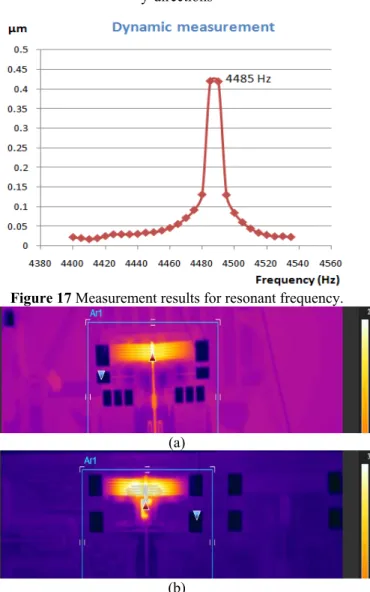
1.42μm (Figure 15). The experimental decoupling ratio in the two directions was 19.24, which conforms to the minimum system requirement of 10. Figure 16 presents displacement variation with driving voltage. The MMA system was also used in the dynamic characterization to evaluate the resonant frequency of the proposed image stabilizer. Figure 17, which plots the measurements, shows that resonant frequency is approximately 4485 Hz.
Figure 18 shows the measurement results for thermal imaging. The red and blue triangles represent the maximum and the minimum temperatures of actuator when 10 volts is supplied in 1 Hz. The figure shows that the maximum temperature occurs in the middle of the actuator and the pads approach room temperature, besides, after comparing figure 18(a) and (b), we can observe the maximum temperature of thermal actuator without isolator is about 290。C (figure 18(a)), and about 360。C of the thermal actuator which connects with isolator (figure 18(b)), so we can use lower driving voltage to achieve the same actuating displacement by using isolator design.
Figure 16 Static measurement of XY-stage in x- and y-directions
Figure 17 Measurement results for resonant frequency.
(a)
(b)
Figure 17 Measurement results for thermal imaging in 10 volts 1Hz. (a) Thermal actuator without isolator. (b) Thermal actuator with isolator.
五、 結論與討論
An integrated micro decoupling XY stage is designed and fabricated. The integrated XY stage is designed to load an image sensor. It can be applied in commercial cell phone cameras as an anti-shake system. This proposed device is mainly composed of a silicon-based XY stage, a comb actuator and a chevron thermal actuator, which are fabricated by SOI wafer with ICP etching process. Precise calculation of the ICP etching rate and a favorable structure layer design can increased the yield of the fabrication process. A stopper and isolator SU8 are effectively prevent pull-in and thermal conductive problems. The actuating displacements of electrostatic and thermal XY stage are all fit the project requirement 25μm and the decoupling ratio are 59 and 19, which are larger than the project requirement 10 so that the structures can avoid the lateral movement when the stages are actuated.
六、 參考文獻
[1] Lining Sun, Jiachou Wang, Weibin Rong, Xinxin Li and Haifei Bao ,A silicon integrated micro nano-positioning XY-stage for nano-manipulation, J.
Micromech. Microeng. 18 (2008), 125004
[2] Kazuhiro Takahashi, Makoto Mita, Hiroyuki Fujitaand Hiroshi Toshiyoshi, A high fill-factor comb-driven XY-stage with topological layer switch architecture,
IEICE Electron. Express 3 (2006), 197-202
[3] H. N. Kwon, J.-H. Lee, K. Takahashi, and H. Toshiyoshi, Micro XY Stages with Spider-leg Actuators for Two-dimensional Optical Scanning,” Sens. Actuator
A-Phys. 130-131 (2006), 468–77
[4] S. Kwon and L.P. Lee, Stacked Two Dimensional Micro-lens Scanner for Micro Confocal Imaging Array,
Proc. IEEE MEMS '02 (2002), pp 483-6
Towards integration of glass microlens with silicon comb-drive X-Y microstage, IEEE/LEOS Int. Conf. on
Optical MEMS and Nanophotonics (2008), pp168-9
[6] K. Y. Yasumura, J. D. Grade, and H. Jerman, Fluid Damping of an Electrostatic Actuator for Optical Switching Applications, Proc. Solid-State Sensor,
Actuator and Microsystems Workshop (2002), pp 358-61
[7] K. Takahashi, H. N. Kwon, M. Mita, K. Saruta, J.-H. Lee, H. Fujita, and H. Toshiyoshi, A silicon micromachined f-θ microlens scanner array by double-deck device design technique, IEEE J. Sel. Top.
Quantum Electron. 13 (2007), 277-82
[8] J. P. Yang, J. Q. Mou, N. B. Chong, Y. Lu, H. Zhu, Q. Jiang, W. G. Kim, J. Chen, G. X. Guo and E. H. Ong, Probe recording technology using novel MEMS devices,
Microsyst. Technol. 13 (2007), 733-40
[9] Ando Y, Development of three-dimensional electrostatic stages for scanning probe microscope,
Sensors Actuators A 114 (2004), 285–91
[10] Indermuhle P F, Linder C, Brugger J, Jaecklin V P and de Rooij N F, Design and fabrication of an overhanging XY-microactuator with integrated tip for scanning surface profiling, Sensors Actuators 43 (1994), 285–91
[11] Kawai Y, Ono T, Esashi M, Meyer E and Gerber C, Resonator combined with a piezoelectric actuator for chemical analysis by force microscopy, Rev. Sci. Instrum. 78 (2007), 063709
[10] Vancura C, Ruegg M, Li Y, Lange D, Hagleitner C, Brand O, Hierlemann A and Baltes H, Magnetically actuated CMOS resonant cantilever gas sensor for volatile organic compounds, Proc. 12th Int. Conf. on Solid State
Sensors, Actuators and Microsystems (2003), pp 1355–8
[11] Sasaki, Bono F and Hane K, XY-stage for scanning media for optical data storage, Proc. IEEE Optical MEMS
and Their Applications (2006), pp 36– 7
[12] Kim C H, Jeong H M, Jeon J U and Kim Y K, Silicon micro XY-stage with a large area shuttle and no-etching holes for SPM-based data storage, J. Microelelctrmech.
Syst. 12 (2003), 470-8.
[13] Lu M S-C and Fedder G K, Position control of parallel-plate microactuators for probe-based data storage, J. Microelectromech. Syst. 13 (2004), 759–9
[14] Liu X, Kim K and Sun Y, A MEMS stage for 3-axis nanopositioning, J. Micromech. Microeng. 17 (2007), 1796–2
[15] Mukhopadhyay D.; J. Dong, J.; Pengwang, E. and Ferreira, P. M., A SOI MEMS based 3-DOF Planar Parallel-Kinematics Nanopositioning Stage, Sens.
Actuators, A 147 2008), 340–51.
[16] Lei Gu, Xinxin Li, Haifei Bao, Bin Liu, YuelinWang, Min Liu, Zunxian Yang and Baoluo Cheng, Single-wafer-processed nano-positioning XY-stages with trench-sidewall micromachining technology, J. Micromech.
Microeng. 16 (2006), 1349–57
[17] D. H. Yeom, N. J. Park, and S. Y. Jung, Digital controller of novel voice coil motor actuator for optical image stabilizer, Int. Conf. on Control, Automation and Systems (2007), pp 2201
[18] K. Sato, S. Ishizuka, A. Nikami, and M. Sato, Control techniques for optical image stabilizing system, IEEE
Trans. Consum. Electron. 39 (2005), 461-66
[19] Yasuhiro Okamoto and Ryuichi Yoshida, Development of linear actuators using piezoelectric elements, Electron. Commun. Jpn. Pt. III 81 (1998), 11-7 [20] Guan-Rong Chen, Yeou-Min Yeh, Sheng-Jyh Wang, and Huang-Cheng Chiang, A novel structure for digital image stabilizer, IEEE Asia-Pacific Conf. on Circuits and
Systems (2000), pp 101-104
[21] Mohamed A, Elsimar H and Ismail M, Analysis, and optimization of a CMOS vertical thermal actuator, Proc.
Symp. Design, Test, Integration and Packaging of MEMS/MOEMS (2003), pp 214-7
[22] S. E. Alper and T. Akin, A Single-Crystal Silicon Symmetrical and Decoupled MEMS Gyroscope on an Insulating Substrate, J. Microelectromech. Syst. 14 (2005), 707-17
[23] W. C. Tang, T.-C. H. Nguyen, and R. T. Howe, Laterally Driven Polysilicon Resonant Microstructures,
Proc. IEEE Micro Electro Mechanical Systems (1989), pp
[24] Legtenberg R, Groeneveld A W and Elwenspoek M, Comb-drive actuators for large displacements, J.
Micromech. Microeng. 6 (1996), 320-9
[25] D. Sachs, S. Nasiri, and D. Goehl: Image Stabilization Technology Overview
[ http://www.invensense.com/shared/pdf/ImageStabilizatio nWhitepaper_051606.pdf ].
[26] Chih-Chun Lee, Wen-Chih Chen, Sz-Yuan Lee and Weileun Fang, Design and Implementation of a novel polymer joint for thermal actuator current and thermal isolation, IEEE MEMS conference (2010), page.156-159. [27] L.Que, J.-S. Park, and Y.B. Gianchandani, Bent-Beam Electro-Thermal Actuators For High Force Applications, Journal of Micro Electro Mechanical
Systems (1999), pp. 31-36.
[28] Chun-Ying Lin, Jin-Chern Chiou, Design, Fabrication and Actuation of 4-axis Thermal Actuating Image Stabilizer, Micro & Nano Letters, Vol. 6, Iss. 7, (2011), pp. 549–552
國科會補助專題研究計畫項下出席國際學術會議心得報告
日期:100 年 5 月 10 日一、參加會議經過
2011 IEEE International Instrumentation and Measurement Technology Conference 是
IEEE 對於量測研究相當重要的研討會,由於指導教授邱俊誠教授的鼓勵與支持,本
人將所做之紅外線溫度計的研究成果整理成篇,於 2010 年十月向此會議投稿摘要,
在經過兩個月審核確定此篇文章為以口頭發表的形式發表,由於此次為口頭方式發
表,本人也多次在所屬實驗室每週開會時上台講述增加練習經驗,也聽取許多老師
與同學多方的建議,才完成此次出發前往中國的事前準備。
計畫編號 NSC
99-2220-E-009-044
計畫名稱
微機電防手振平台之設計、製作與測試
出國人員
姓名
侯冠州
服務機構
及職稱
交通大學電控所,博士班六年級
會議時間
2011 年 5 月 10 日至
2011 年 5 月 12 日
會議地點
大陸杭州
會議名稱
(中文) 2011 IEEE 國際量測技術研討會
(英文) 2011 IEEE International Instrumentation and Measurement
Technology Conference
發表論文
題目
(中文) 電校式輻射量測方法與建立
(英文)
Development of Absolutely Radiant Flux Measurements with
Electrical Calibrated Microbolometer (ECuB)
二、與會心得
此會議為量測領域相當重要的大型國際會議,在準備報告的過程中,不論是服裝
儀容與外語能力,都在出發前多做準備,本人到會場報到時感受到會議人員的專業
與大會的用心,所有的資料都用個人的方式包裝,會議人員也都親切相待,會議期
間每天都有相當多場的口頭論文發表,我會選取對於個人相關研究有關或對其題目
有興趣的場次去聆聽,包含雷射控制、薄膜製作與感測器應用的場次。藉由發表者
的論文加強我感測技術領域知識與相當多的思考方向,由於先前準備充足發表過程
相當順利,發表後的五分鐘問答時間由主持人提出建議,對我的實驗相當有助益,
讓我覺得此次會議是趟非常值得的行程。
三、考察參觀活動(無是項活動者略)
四、建議
參加此類國際知名大型研討會,不僅可以了解世界上相同領域的研究方向以及研究
深度之外,並且能提升研究水準與拓展國際視野,因此有志於長期研究的學者或是
研究生更應鼓勵多參與國際性的研討會,藉由和與會的學者互相討論也可以激發出
不錯的研究想法。所以,若能夠持續在經費上得到國科會的適當補助,對於研究學
者或是研究生將會有極大的幫助。
五、攜回資料名稱及內容
會議摘要集一本:內容包含會議所有投稿之摘要
六、其他
國科會補助計畫衍生研發成果推廣資料表
日期:2011/10/27國科會補助計畫
計畫名稱: 子計畫一:微機電防手振平台之設計、製作與測試(3/3) 計畫主持人: 邱俊誠 計畫編號: 99-2220-E-009-002- 學門領域: 晶片科技計畫--整合型學術研究 計畫無研發成果推廣資料
99 年度專題研究計畫研究成果彙整表
計畫主持人:邱俊誠 計畫編號: 99-2220-E-009-002-計畫名稱:創新異質整合智慧型手機相機模組之研究--子計畫一:微機電防手振平台之設計、製作與 測試(3/3) 量化 成果項目 實際已達成 數(被接受 或已發表) 預期總達成 數(含實際已 達成數) 本計畫實 際貢獻百 分比 單位 備 註 ( 質 化 說 明:如 數 個 計 畫 共 同 成 果、成 果 列 為 該 期 刊 之 封 面 故 事 ... 等) 期刊論文 0 0 100% 研究報告/技術報告 0 0 100% 研討會論文 0 0 100% 篇 論文著作 專書 0 0 100% 申請中件數 0 0 100% 專利 已獲得件數 0 0 100% 件 件數 0 0 100% 件 技術移轉 權利金 0 0 100% 千元 碩士生 1 1 100% 博士生 1 1 100% 博士後研究員 0 0 100% 國內 參與計畫人力 (本國籍) 專任助理 0 0 100% 人次 期刊論文 3 2 100% 研究報告/技術報告 0 0 100% 研討會論文 2 2 100% 篇 論文著作 專書 0 0 100% 章/本 申請中件數 0 0 100% 專利 已獲得件數 0 0 100% 件 件數 0 0 100% 件 技術移轉 權利金 0 0 100% 千元 碩士生 1 2 100% 博士生 3 2 100% 博士後研究員 0 0 100% 國外 參與計畫人力 (外國籍) 專任助理 0 0 100% 人次其他成果