國立交通大學
生物醫學研究所
碩士論文
元件製程對於多晶矽奈米線場效電晶體水測電性影
響之分析
Fabrication Process and its Effects on the Electric
Characteristics of Poly Crystalline Silicon Nanowrie Field Effect
Transistor in Aqueous Solution
研究生:魏若芬
指導教授:楊裕雄 博士
元件製程對於多晶矽奈米線場效電晶體水測電性影響之分析
Fabrication Process and its Effects on the Electric Characteristics of
Poly Crystalline Silicon Nanowrie Field Effect Transistor in
Aqueous Solution
研究生:魏若芬 Student:Jo-Feng Wei
指導教授:楊裕雄 博士 Advisor:Dr. Yuh-Shyong Yang
國 立 交 通 大 學
生 物 醫 學 研 究 所
碩 士 論 文
A Thesis
Submitted to Institute of Biomedical Science College of Biological Science and Technology
National Chiao Tung University in partial Fulfillment of the Requirements
for Degree of Master of Science in
Biomedical Science
June 2009
Hsinchu, Taiwan, Republic of China
元件製程對於多晶矽奈米線場效電晶體水測電性影響之分析
研究生:魏若芬 指導教授:楊裕雄 博士
國立交通大學
生物科技學院
生物醫學所
摘 要 多晶矽奈米線場效電晶體生物感測器使用電訊號偵測生物分子具有極高靈敏度、即 時偵測及無需標記物之優點。儘管矽奈米線場效電晶體具有以上的優勢,但是典型測試 在水溶液電性變化影響之研究卻極少探討。在這裡,我們研究如何製作多晶矽奈米線場 效電晶體以改善元件於水溶液環境下量測之電訊號穩定性。多晶矽奈米線場效電晶體於 背閘極上,我們個別堆層二氧化矽及氮化矽兩種材料絕緣層及分析些兩種元件之電性號 變化。同時使用新穎微流道保持水中環境並討論不同長度、不同條數之矽奈米線場效電 晶體之水中電性測試。發現兩種材料作為絕緣層都具有極高的靈敏度與於水中測試之穩 定度。最後,由於奈米線為矽材質,因此我們使用未固定化及固定化後之奈米線氮化矽 作絕緣層元件測量不同pH值之PBS之關係。Fabrication Process and its Effects on the Electric Characteristics of Poly
Crystalline Silicon Nanowrie Field Effect Transistor in Aqueous Solution
Student:Jo-Fen
Wei Advisor:Dr. Yuh-Shyong Yang
Department of Biomedical Science National Chiao Tung University
Abstract
Biosensors based on silicon nanowires promise real-time, highly sensitive and label-free
electrical detection of biomolecules. Despite the tremendous potential and promising
experimental results, the fundamental mechanisms of electrical sensing in aqueous
environment remain poorly understood. In this work, we investigated how the fabrication
process can help to improve the reliability of poly-Si nanowire filed-effect transistor (NWFET)
in aqueous solution. Dielectric layers, silicon oxide or nitride, was prepared on the top of back
gate in poly-Si NWFET and their effects on device characteristics were determined. The
poly-Si NWFET was also prepared with variations of the number and length of the nanowires.
The results indicated that either nitride or oxide dielectric layers as insulator improved the
stability of poly-Si NWFET devices in aqueous solution. Finally, the pH effect on the electric
properties of poly-Si NWFET was further investigated using unmodified and APTES
致 謝
兩年半的研究生生涯對我來是一項大試煉,由於是跨領域學習,因此這段時 間受到很多人的幫助。在修課及實驗的低潮期中總是可以聽到同學間互相鼓勵、 打氣說:『加油』。聽到這句話後就可以帶著滿滿的信心把事情做完、做好。所 以在研究生生活裡,我除了學習到寶貴的研究經驗外,更得到更多珍貴的友情。 以及實驗室學長們對我這兩年半來照顧,因為你們讓我體會如何謙卑學習的心 態、懂得心存感激、做任何一件事情不到最後別放棄…在此,我致上最誠心的感 謝。 在此期間除了感謝我的指導教授 楊裕雄老師在學術與學術倫理方面的細心 教導外,更感謝老師給我充足的實驗資源,讓我能進儀科中心、國家奈米元件實 驗室(NDL)學習,並且給我自主學習的能力與及時的引導;同時感謝 林鴻志老師 對我實驗上的一些寶貴意見及其研究室同學、學長、學弟、學妹在實驗上給予的 幫助及鼓勵。還有國家實驗研究院 儀器科技研究中心提供專業的指導及NDL提 供儀器及專業的工程師們,讓我們能夠在優質的環境下製作元件。 感謝電子所的維濤學弟提供論文修改寶貴的意見、行徽學長的細心指導、感 謝小米學姐在實驗上給很多寶貴的學習經驗。在跨領域的學習階段中,特別的感 謝宜貞及敏書同學一路上的貼心的鼓勵;感謝家人這兩年來的支持讓我無後顧之 憂將碩士念完,以及過多提不完的你們。 你們是讓我完成碩論這個小成就中的最大推手,謝謝你們…同時,能夠認識 你們,真是我的榮幸! 交通大學 生物醫學所 魏若芬 謹上CONTENTS
Abstract (in Chinese) Ⅰ
Abstract (in English) Ⅱ
Acknowledgments (in Chinese) Ⅲ
Contents Ⅳ
Tables & Figure Captions Ⅴ
CHAPTER1:INTRODUCTION... 1
1-1 BACKGROUND... 1
1-2MOTIVATION... 2
REFERENCES:...4
CHAPTER 2:MEASUREMENT SETUP AND MICROFLUID SYSTEM ...7
2-1MICROFLUIDICS FABRICATION... 7
2-2METHOD OF DEVICE PARAMETER EXTRACTION... 8
2-2-1 Determination of the Threshold Voltage [3]... 8
2-2-2 Determination of Subthreshold Swing ... 10
2-2-3 Determination of the On/Off Current Ratio ... 10
REFERENCES: ...12
CHAPTER 3:FABRICATION AND ELECTRICAL CHARACTERIZATION OF NANOWIRE TRANSISTORS ...16
3-1DEVICE STRUCTURES AND FABRICATION... 16
3-2EFFECT OF ELECTRIC PROPERTIES OF DEVICE IN EITHER WATER OR AIR... 19
3-3EFFECT OF CHANNEL LENGTH AND NUMBER ON THE ELECTRIC PROPERTIES OF POLY NWFETS... 20
3-4SENSING MEASUREMENTS OF PHPBSUSING POLY-SI NWFETS... 21
REFERENCES:...24
Table Captions
Chapter 1
TABLE 1-1COMPARISON CHART WITH VARIOUS SENSING METHODS.[21]... 6
Chapter 2
TABLE 2-1:PHYSICAL AND CHEMICAL PROPERTIES OF PDMS ... 15
Chapter 3
TABLE 3-1:SUMMARIZES THE MEASURED AND EXTRACTED PARAMETERS OF NORMALIZED ON
CURRENT FROM THE DEVICE C(CHANNEL LENGTH =2UM,VG-VTH=0.7V,VD=0.5V)... 35
TABLE 3-2:SUMMARIZES THE MEASURED AND EXTRACTED PARAMETERS FROM THE DEVICE C.
Figure Captions
Chapter 2
FIGURE 2-1:THE DIAGRAM IS THE CROSS-SECTION OF MICROFLUIDICS APPARATUS. ... 13
FIGURE 2-2:MICROFLUIDICS APPARATUS... 13
FIGURE 2-3: SEMI-STRUCTURAL FORMULA OF PDMS. ... 14
FIGURE 2-4: AMOSFET WITH SOURCE AND DRAIN RESISTANCES [3] ... 14
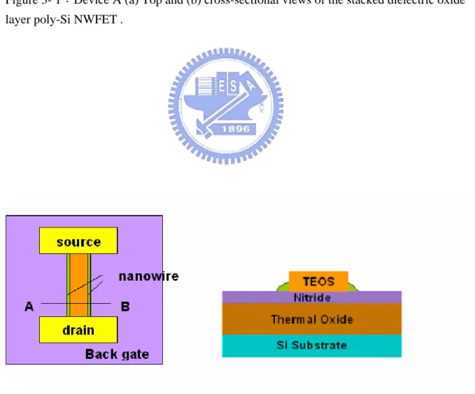
Chapter 3 FIGURE 3-1:DEVICE A(A)TOP AND (B) CROSS-SECTIONAL VIEWS OF THE STACKED DIELECTRIC OXIDE LAYER POLY-SI NWFET... 25
FIGURE 3-2:DEVICE B(A)TOP AND (B) CROSS-SECTIONAL VIEWS OF THE STACKED DIELECTRIC NITRIDE AND OXIDE LAYER POLY-SINWFET. ... 25
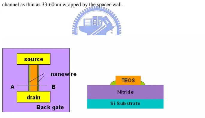
FIGURE 3-3: (A)TOP AND (B) CROSS-SECTIONAL SEM IMAGES OF POLY-SI NWFET WHICH NW CHANNEL AS THIN AS 33-60NM WRAPPED BY THE SPACER-WALL. ... 26
FIGURE 3-4:DEVICE C(A)TOP AND (B) CROSS-SECTIONAL VIEWS OF THE STACKED DIELECTRIC NITRIDE LAYER POLY-SI NWFET. ... 26
FIGURE 3-5:THE PROCESS STEPS FOR MEASUREMENT OF THE ELECTRICAL PROPERTIES OF THE NANOWIRE DEVICES... 27
FIGURE 3-6:THE ELECTRICAL PROPERTIES OF THE STACKED DIELECTRIC OXIDE LAYER POLY -SI NWFET(DEVICE A) MEASURING IN THE AIR AND WATER. ... 27
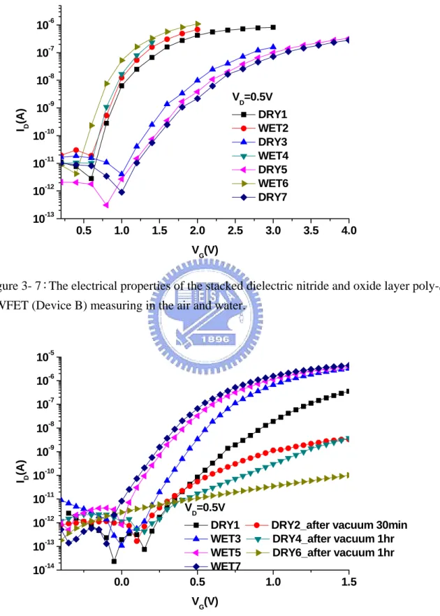
FIGURE 3-7:THE ELECTRICAL PROPERTIES OF THE STACKED DIELECTRIC NITRIDE AND OXIDE LAYER POLY-SI NWFET(DEVICE B) MEASURING IN THE AIR AND WATER... 28
FIGURE 3-8:THE ELECTRICAL PROPERTIES OF THE STACKED DIELECTRIC NITRIDE LAYER POLY-SI NWFET(DEVICE C) MEASURING IN THE AIR AND WATER. ... 28
FIGURE 3-9:TRANSFER CHARACTERISTICS OF THE PROPOSED THE STACKED DIELECTRIC NITRIDE LAYER POLY-SI NWFET(DEVICE C) WITH DIFFERENCE CHANNEL THAT MEASURES IN THE AIR. ... 29
FIGURE 3-10:TRANSFER CHARACTERISTICS OF THE PROPOSED THE STACKED DIELECTRIC NITRIDE LAYER POLY-SI NWFET(DEVICE C) WITH DIFFERENCE LENGTH THAT MEASURES IN THE AIR. ... 29
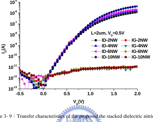
FIGURE 3-11:TRANSFER CHARACTERISTICS OF THE PROPOSED THE STACKED DIELECTRIC NITRIDE LAYER POLY-SI NWFET(DEVICE C) WITH DIFFERENCE LENGTH THAT MEASURES IN THE WATER. ... 30
FIGURE 3-12:TRANSFER CHARACTERISTICS OF THE PROPOSED THE STACKED DIELECTRIC NITRIDE LAYER POLY-SI NWFET(DEVICE C) WITH DIFFERENCE LENGTH THAT MEASURES IN THE WATER. ... 30
FIGURE 3-13:REAL-TIME DETECTION OF THE DRAIN CURRENT FOR UNMODIFIED POLY-SI NANOWIRE FOR DIFFERENCE PHPBS(10MM)... 31
FIGURE 3-14:REAL-TIME DETECTION OF THE DRAIN CURRENT FOR UNMODIFIED POLY-SI NANOWIRE FOR DIFFERENCE PHPBS(10MM)... 31
FIGURE 3-15:REAL-TIME DETECTION OF THE DRAIN CURRENT FOR APTES MODIFIED POLY-SI
NANOWIRE FOR DIFFERENCE PHPBS(10MM)... 32
FIGURE 3-16:THE MICROFLOW SYSTEM. ... 32
FIGURE 3-17:SCHEMATICS DIAGRAM OF THE INTERFACIAL CHARGE TRAPPING MECHANISM IN
WHICH -SIOH IS DEPROTONATED TO –SIO-.[10]... 33
FIGURE 3-18:SCHEMATICS DIAGRAM OF THE INTERFACIAL CHARGE TRAPPING MECHANISM.
ZOOM OF THE APTES-MODIFIED SINW SURFACE.[7] ... 33
FIGURE 3-19:TRANSFER CHARACTERISTICS OF SS OF DEVICE C AS A FUNCTION OF CHANNEL
LENGTH. ... 34
Appendix
APPENDIX1:THE PROTOCOL FOR PREPARE 10MMPBS WITH DIFFERENCE PHPBS... 37 APPENDIX2:DEFINED THE KA AND PKA... 37
APPENDIX3:THE PROTOCOL OF MODFIED THE POLY-SI NANOWIRE WITH APTES ... 38 APPENDIX4:THE PKA OF SILICON NITRIDE... 39 Abbreviation
Poly Si Poly Silicon
Single Si Single Silicon
PDMS Poly -(DiMethylSiloxane)
PBS Phosphate Buffer Saline
pKa Acid dissociation constant
NW NanoWire
Chapter 1:Introduction
1-1 Background
There is increased demand for the availability of simple and reliable protocols for the
analysis of molecules of biological importance. The requirement of skilled manpower,
excessive external reagents, complicated sample preparation methods and time-consuming
procedures has limited the applications of most of the known classical techniques for different
bio-species detection (Table 1-1). [21] To address this critical issue, there are many studies in
biosensor recently. Biosensor is an analytical device which transforms the signal resulting
from the interaction of the analytes into the electrical signal that could be more easily
quantified and measured. One of the biosensors, poly-silicon nanowire field effect transistor
(Poly-SiNW FET) is important due to large surface-to-volume ratio, its electrical property
such as conductance is dominated by surface contributions. Therefore, the presence of
charged substance on the surface of an active nanowire induces a large fractional change in
the nanowire conductance and enables relatively easy detection. In other words, it possesses
ultrahigh sensitivity[22]. Besides, poly-Si NW FET is working by the label-free detection due
to the changes in electric response. Furthermore, it has more superior to others because of the
real-time detection.
Poly-Si NWFET can be prepared by either ‘bottom-up’ or ‘top-down’ lithography
lithography tools to generate the NW patterns [13-14]. Although compatible with mass
production, the use of advanced lithography tools is costly. The bottom-up approaches usually
employ metal-catalytic growth for preparation of NWs [15-17]. However, the nanowires are
not easy to manipulate and arrange in order. For device fabrication with lift-off S/D formation,
it is also very difficult to fix the distance between source and drain. Hence, we fabricate
spacer poly-Si NWFET as sensor compatible with mass production as sensing device.
1-2 Motivation
In this work, we utilized a novel approach to release above concerns. The poly-Si
nanowire channels were fabricated by employing the poly-Si sidewall spacer technique,
which approach was comparable with current commercial semiconductor process and
forsaken expensive E-beam lithography tools. Though the poly-Si NWFET possesses
potential application for biological sensing application, there are still some drawbacks. For
instance the electrical characteristics of poly-Si NWFET are mainly influenced by the
defects in the grain boundaries and within the grains [18]. Trap states resulted from those
defects within the channel lead to poor device performance, such as low field effect
mobility, large leakage current [19], large subthreshold slope, and high threshold voltage.
Another issue is the stability for testing in aqueous solution which is very essential for
development of advanced biosensor technology. The design of reliable biological or
charges, requires reducing the influence of any unwanted or uncontrolled potential-induced
charging at the substrate-bio layer interface. Because of the leakage current in the test
solution is unstable during measurements; it may also affect the electrical characteristics of
NW devices. To address this critical issue, we improve water-tested reliability of poly-Si
NWFET by using a stacked dielectric consisting of nitride layer [20]. Besides, we prepare
different pH phosphate buffer saline (PBS) solutions (see in appendix 1) and then measured
the electric portieres of the test devices. The phenomenon of the tested devices is measured
and analyzed.
1.3 Thesis Organization
This thesis is focused on improve the stability of poly-Si NWFET for the measurement
of the electrical property in the water environment .Additionally, we compare the electrical
property of three devices that fabricated by a stacked dielectric either of oxide layer and
nitride layer. This thesis is divided into four chapters.
Chapter 1: Introduce and descript strong points of the spacer NWFET character and some
issues for bio test to improve.
Chapter 2: Review describes the MOSFET classical electrical property definition and the
fabrication of microfluidics is described.
Chapter 3:Detail description of device fabrication and data.
References:
[1]G.M. Laws, T.J. Thornton, Jinman Yang, L.de la Garza, M. Kozicki, D.gust, Phys. Stat.
sol.(b) 233,83-89.
[2] F. Davis, A.V. Nabok, S.P.J. Higson, 2005. Biosens, Bioelectron.20, 1531-1538.
[3] R.J. Mitchell, M.B. Gu, 2004. Biosens. Bioelectron. 19 ,977-985.
[4] Besteman, K., Lee, J., Wiertz, F.G.M., Heering, H.A., Dekker, C., 2003. Nano Lett. 3,
727–730.
[5] Cui, Y.,Wei, Q., Park, H., Lieber, C.M., 2001. Science 293, 1289–1292.
[6] Li, C., Curreli, M., Lin, H., Lei, B., Ishikawa, F.N., Datar, R., Cote, R.J., Thompson,
M.E.,Zhou, C., 2005. J. Am. Chem. Soc. 127, 12484–12485.
[7] Hahm, J., Lieber, C.M., 2004. Nano Lett. 4, 51–54.
[8] Patolsky, F., Zheng, G., Hayden, O., Lakadamyali, M., Zhuang, X., Lieber, C.M., 2004.
PNAS 101, 14017–14022.
[9] Patolsky, F., Zheng, G., Lieber, C.M., 2006c. Nanomedicine 1, 51–65.
[10] Star, A., Tu, E., Niemann, J., Gabriel, J.C.P., Joiner, C.S., Valcke, C., 2006. PNAS 103,
921–926.
[11] Wang,W.U., Chen, C., Lin, K., Fang, Y., Lieber, C.M., 2005. PNAS 102, 3208–3212.
[12]Chen, Y., Wang, X., Hong, M.K., Erramilli, S., Mohanty, P., Rosenberg, C., 2007. Appl.
[13] Lee, K.N., Jung, S.W., Kim, W.H., Lee, M.H., Shin, K.S., Seong, W.K., 2007.
Nanotechnology 18, 445302.
[14] Li, Z., Chen,Y., Li, X., Kamins, T.I.,Nauka, K., Williams, R.S., 2004.Nano Lett. 4,
245–247.
[15] Duan, X., Huang, Y., Lieber, C.M., 2002. Nano Lett. 2, 487–490.
[16] Duan, X., Niu, C., Sahi, V., Chen, J., Parce, J.W., Empedocles, S., Goldman, J.L.,
2003.Nature 425, 274–278.
[17] McAlpine, M.C., Friedman, R.S., Jin, S., Lin, K.H.,Wang,W.U., Lieber, C.M., 2003.
Nano Lett. 3, 1531–1535.
[18] Wu, I. W., Jackson, W. B. T., Huang, Y. A., Lewis, G., and Ciang, A., 1991. IEEE
Electron Device letter 12, 181-183.
[19] Fossum, J. G., Ortiz-Conde, A., Shicjijo, H., Banerjee, abd S. K., 1985. IEEE Trans.
Electron Devices 32, 1878-1882.
[20] Hsiao, C.Y., Lin, C.H., Hung, C.H., Su, C.J., Lo,Y.R. Lee,C.C., Lin, H.C., Ko,F.H.,
Huang,T.Y., Yang,Y.S. 2009. Biosensors and Bioelectronics 24, 1223-1229.
[21] Arora, K., Chand, S.,Malhotra, B.D.,2006. Analytica Chimica Acta ,568, 259-273.
[22]Chen,Y., Wang, X., Erramilli, S., Mohanty, P., 2006. Appl. Phys. Lett.,89. 223512-1-223512-3.
Table 1- 1 Comparison chart with various sensing methods. [21]
Detection technique Assay time Limitations of technique Molecular biological methods /
Biochemical methods
1–3 days Longer assay time Serological tests or Immunological
detection Methods
1–2 days Costly, requirement of monoclonal antibodies, longer assay time, etc. Western blotting 1–2 days Costly, longer assay time, skilled
manpower
Gas sensing methods (GC, HPLC,etc.) 2–3 hr Costly, no on-site measurement
Polymerase Chain Reaction ~2–4 hr No on-site detection, need of enrichment, etc.
Nucleic acid sequence-based Amplification (NASABA)
<1 hr On-site testing can not be performed Immune diagnostic kits Within minutes to hours Costly
DNA probe assay Longer assay time, pre-enrichment, various
pre-experimental preparations, etc. Fourier transform infrared and Raman
spectroscopy
Chapter 2:Measurement Setup and Microfluid System
2-1 Microfluidics Fabrication
We proposed one method to set up our microfluidics that can be reused on different
test chips. The apparatus of the use of the technique is shown in Fig. 2-1. The PDMS
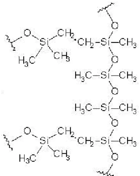
poly-(dimethylsiloxane) has been one the most actively developed polymers for
Microfluidics. The semi-structural formula of this material is show in Fig.2-3. Table 2-1
lists its chemical and physical properties, those which are feasible for fabrication of devices
with useful functionality.
Below is the microfluid system process flow[2]:
1) Maxing PDMS (poly dimethylsiloxane):volume ratio = 10:1 with stirring rod for
5min
2) Use vacuum pump to degas about 20 min until most bubbles are gone
3) Pour it to a mother mode (glass)
4) Cure PDMS at 90°C for 20 min
5) Carefully peel off the PDMS structure
6) Punch input and output holes
7) Surfaces may need to be cleaned with acetone.
8) Bond PDMS microfluid system to nanowire devices
9) Bake with oven at 90°C for 30 min
11) Insert Teflon tubes to inject sample with string pump
12) Test and measure completed samples. (Fig 2-2)
2-2 Method of Device Parameter Extraction
In this thesis, we use N&K1500 to measure the thickness of amorphous-Si, TEOS
oxide and nitride films in the fabrication procedure. All the electrical characteristics of
proposed poly-Si FETs were measured by Keithley 2636 System SourceMeter Instrument.
See the way below that are used for extracting the electrical parameters of the NW devices.
2-2-1 Determination of the Threshold Voltage [3]
For bulk MOSFET, the gate voltage at which the electron density at the interface
is the same as the hole density in the neutral bulk material is called the threshold
voltage [6]. For an n-channel device as the gate voltage is above the threshold voltage,
the transistor is turned on due to the induction of a sheet of electrons in the channel at
the oxide-silicon interface creating a low-resistance channel where charges can flow
from drain to source.
For NW devices, the body effect can be ignored, and the MOSFET
current-voltage equation is )] ( ))][ ( ( 5 . 0 [ GS T D s DS D s D DS D s D D kV V I r V I r r V I r r I = − − − − + − + (2-1),
where rS and rD are defined in Fig. 2-4. Threshold voltage can be extracted using the
linear extrapolation method. In this method, the drain current is measured as a function
of gate voltage at a low drain voltage (typically 50mV) to ensure operation in the linear
MOSFET region. Because of series resistance is usually negligible at the low drain
currents where threshold voltage measurements are made. According to Eq. (2-1), as
the drain current is zero, we can express Eq. (2-2) in terms of VGS and VD:
0 5 . 0 = − − T D GS V V V (2-2).
But Eqs. (2-1) and (2-2) are valid only above threshold. The drain current is not zero
below threshold and approaches zero only asymptotically. Hence in this method the ID
verus VGS curve is extrapolated to ID=0 and the threshold voltage is determined from
the extrapolated or intercept gate voltage VGSi by
2 DS GSi T V V V = − (2-3).
In this work, we use another way which is simpler than the complex linear extrapolation
method to extract the threshold voltage. In this method, the threshold voltage is defined
as the gate voltage as the drain current is specified at (W/L) ×10nA for VDS=0.1V and
(W/L) ×100nA for VDS=5V, where W and L are channel width and channel length,
2-2-2 Determination of Subthreshold Swing
Subthreshold swing, S.S. (V/dec), is a typical parameter to describe the control
ability of gate voltage. For an ideal switch device, it is turned off as the gate voltage is
below the threshold voltage and ideally there is no current from the drain to the source.
In reality, there is a current, dubbed subthreshold current (or leakage), flows along the
channel although it is relatively small and varies exponentially with gate bias.
Subthreshold swing is defined as the amount of gate-voltage shift required to modulate
the subthreshold current by one oreder of magnitude. The exact S.S. can be extracted
using the following formula: [4]
1 ) ( 10 ) log ( − ∂ ∂ = G I V SS D (2-4).
According to Eq.(2-4), the lower the S.S. is, the better the gate controllability does. For
bulk CMOS devices, the value typically falls in the range from 60 to 90mV/dec. For
polycrystalline-channel devices, however, the value is typically much larger due to the
existence of abundant defects in the channel.
2-2-3 Determination of the On/Off Current Ratio
High On/Off ratio represents high signal (on current) to noise (off-state leakage
current) immunity. In this study, the on(drive) current and off(leakage) current are
The leakage current is considered as one of the main problems on poly-Si NWFET.
Because of the poly-Si NWFET is composed of polycrystalline channels which contain a
large amount of defects in grain boundaries. These defects serve as trap states for
conduction carriers in energy band gap. As the device is turned off and the voltage
difference between the gate and drain is sufficiently high, those traps act as centers to
enhance band-to-band tunneling process and thus the off-state current. Therefore there
are many studies in poly-Si to improve the grain structure [7-8]. Here we defined the
on/off ration as blow.
0.5V V at plot V -I of current Min. 0.5V V at plot V -I of current Max. DS GS DS DS GS DS = = = OFF ON I I (2-5).
References:
[1]Mc Donald, J., Whitesides, G., 2002 Accounts of chemical research, 35,491-499.
[2]Wang, T.M. (2007, June). “Study of nanowires thin-film-transistor for biochemical sensor
applications”,National Chiao Tung University, Hsinchu.
[3]Schroder, D.K. (1990), “Semiconductor material and device characterization,” John Wiley
& Sons, New York, pp 81-82.
[4]Cristoloveanu, S., Blalock, B., Allibert, F., Dufrene, B.M., and Mojarradi, M.M., “The
Four-Gate Transistor,” Proc. ESSDERC’02, 323-326, 2002.
[5]Levinson, J., Shepherd, F. R., Scanlon, P. J., Westwood, W. D., Este, G., and Rider,
M.,1982. J. Appl. Phys.,53, 1193–1202.
[6] Sze, S. M.,(1981), "Physics of semiconductor devices" 3rd edition, John Wiley & Sons,
New York, pp 312.
[7] Song, I.H., Kim, C.H., Nam,W.J., and Han, M.K.,2002. in IEDM Tech. Dig., pp. 561–564.
Figure 2- 1:The diagram is the cross-section of Microfluidics apparatus.
Figure 2- 3: Semi-structural formula of PDMS.
Table 2- 1:Physical and Chemical Properties of PDMS
Property Characteristic Density Around 0.9kg/m3
Optical Trnsparent, between 300nm and 2200nm Electrical Insulating, breaking filed 20kV/cm Mechanical Elastomeric, Young’s modulus ~ 750kPa
Thermal Insulating, thermal conductivity ~0.2W/m/K Interfacial Low surface energy (~20 mN/m)
Permeability Permeable to gas, apolar organic solvents, nearly impermeable to water Reactivity Inset, oxidizable by plasma
Chapter 3:Fabrication and Electrical Characterization of Nanowire
Transistors
The silicon surface, after a wet treatment or an oxidation step, appears hydrophilic.
Actually as a Si wafer is placed in a normal environment an oxide layer with thickness
between 0.6 and 2nm would be formed at the surface. However, quality of this native oxide is
poor with typical dangling bond defect density in the range of 1012 cm-2 at Si/oxideinterface.
The defect densities reported are about two orders of magnitude higher than that for thermal
oxides. [1] In our work, the poly-Si nanowaires expose either in the air or in the solution
directly. That will produce native oxide which may bring about concerns about the traps and
associated leakage issue. In this chapter, we state the fabrication process and electrical
characteristics of poly-Si NWFET with variations of the number and length of the nanowires
such as on current, subthreshold swing, threshold voltage in the environment that either in the
air or solution. We can see the on current is simply proportional to the number of NW
channels.
3-1 Device Structures and Fabrication
Our experiments employed NWFETs fabricated on 6-inch p-type wafer capped with a
dielectric layer, either a thermal oxide layer or a nitride/oxide stacked layer. Figs. 3-1(a) and
respectively, of the device, dubbed as device A, formed on the thermal oxide layer. Similar
views for the device, denoted as Device B, formed on a nitride/oxide stacked layer are shown
in Fig. 3-2. In these devices the poly-Si NWs are formed by means of sidewall spacer etching
technique.
In Fig.3-1, the fabrication began on Si wafers capped with a 100 nm-thick thermal oxide.
Next, a 100nm-thick nitride layer was deposited by low-pressure chemical vapor deposition
(LPCVD). After deposition of the nitride layer, standard photolithographic and etch steps
were performed to form the nitride dummy structures. Subsequently, a 100nm-thick
amorphous-Si layer was deposited and then anneal at 600°C for 24hr in N2 ambient to
transform it into polycrystalline. Afterwards, source/drain (S/D) doping was done with
phosphorus ion implantation with a dose of 5E15cm2. After the generation of S/D photoresist
patterns with a lithographic step, a reactive plasma etching step was performed to form the
S/D regions. Owing to the anisotropic etching process, poly-Si NW channels were formed at
the nitride dummy structure simultaneously during the S/D etching step. By carefully
controlling the etching time, the cross-sectional dimensions of poly-Si NW channels can be
easily reduced to sub-100 nm scale. Subsequently, all devices were then covered with a
200-nm-thick TEOS oxide passivation layer. Finally, removed by a 2-step dry/wet etching
process to expose the poly-Si NW.
Because of device could be short in our water tested.
Fabrication of device B began on Si wafers capped with a 100nm-thick thermal
oxide. First 50nm-thick nitride and 100nm-thick TEOS oxide layers were sequentially
deposited by LPCVD. Next was the formation of the TEOS dummy structure. Subsequently,
the 100nm-thick amorphous-Si layer was deposited on the dummy gate and anneal at 600°C
for 24hr in N2 ambient to transform poly-Si respectively. Then source/drain (S/D) doping was
performed with phosphorus ion implantation with a dose of 5E15cm2. After the generation of
S/D photoresist patterns with a lithographic step, a reactive plasma etching step was
performed. Owing to the anisotropic etching process, poly-Si NW channels by the side of the
nitride were formed simultaneously during the S/D etching step. Subsequently, all devices
were then covered with a 200-nm-thick TEOS oxide passivation layer. Finally, removed by a
2-step both dry and wet etching process to expose the poly-Si NW. The cross-sectional and
top SEM images of a poly-Si NWFET with NW channels as thin as 33nm to 60 nm are shown
in Fig.3-3(a) and (b), respectively.
In this work the substrate serves as the bottom-gate for electrical measurements of the
NW devices. Thickness and quality of the dielectric layer capped on the Si wafer would thus
affect the device performance. For more flexibility, we also fabricated device C which has a
150nm-thick nitride layer as the capping insulator. Its structure is shown in Figs. 3-4 (a) and
(a)), respectively, of the device.
3-2 Effect of Electric Properties of Device in either Water or Air
It is known that the existence of grain boundaries within the poly-Si channel region has
great influence on the electrical characteristics of poly-Si device. [2] Those defects may act as
trap centers for conductive carriers and give rise to potential barriers which impede the flow
of current from one grain to another. [3] For biological sensors, the defects could also affect
the sensitivity degradation.In a recent paper the water passivation effect was reported to
reduce such influence while the poly-Si NWFET is immersed and operated in the water
environment [4]. The DI water possesses abundant H+ and /or OH- which may diffuse into the
grain boundaries and terminate on the dangling bonds wherein. [4] Such action may passivate
the defects and thus the electrical characteristics are improved.
Here, we investigate the phenomenon by comparing the electrical characteristics of the
poly-Si NWFET measured either in the water or in the air. Figure 3-5 shows the process flow
of the test. The characteristics (IDS-VGS) of device A, device B and device C measured in
various environments are shown in Fig. 3-6, Fig. 3-7 and Fig. 3-8, respectively (VD=0.5V). As
can be seen in the figures, the electrical characteristic of the poly-Si NWFET in the water is
significantly improved in terms of reduced threshold voltage and subthreshold swing.
Therefore, we believe that trap states were effectively reduced by water passivation. As the
vacuum treatment is 30 min. It is clearly seen that the threshold swing is significantly higher
than that before vacuuming that shown in Fig. 3-19. We suspect that the vacuum treatment
tends to draw out the hydrogen atoms from the poly-Si; therefore the device characteristics
are degraded. For fresh devices, some hydrogen species which has been contained in the
poly-Si are believed to come from the underlying SiN which was deposited with H-related
reaction gas (e.g., SiH4 and NH3), thus abundant of hydrogen atoms are incorporated in the
SiN film [5]. Portion of the H species diffuse into the poly-Si nanowire and passivate the
defects existing therein in the subsequent process steps, thus the fresh device show improved
performance. Owing to the high difference in pressure between the environment and the grain
boundary space that hydrogen may desorbs and release to the environment, thus the device
performance is dramatically degraded. As the test device is placed in the water, the water
passivation occurs to recover and improve the device characteristics.
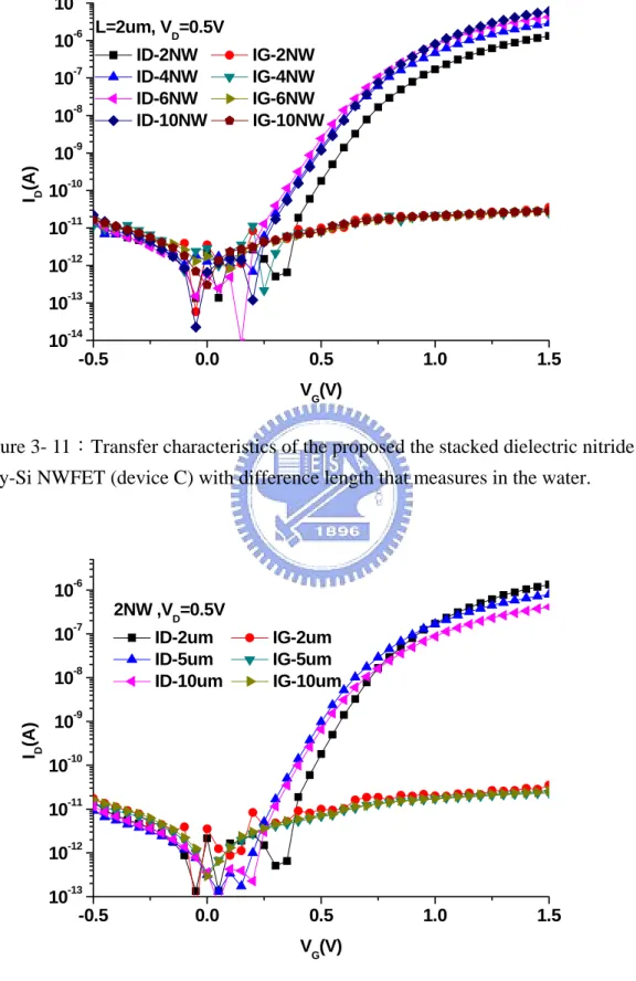
3-3 Effect of Channel Length and Number on the Electric Properties of Poly NWFETs
Figure 3-9 to Fig. 3-12 show the measured results of device C. Figure 3-9 and Fig.
3-11 show the transfer characteristics (IDS-VGS) of devices with different channel number
measured in the air and water, respectively. The summary of normalized drain current as
function of channel number (to a single-channel device) is shown in Fig.3-9 and
summarized in Table 3-1. The normalized on current is extracted at VG-Vth = 0.7V and
NW channels, indicating that the NW channels exhibit stable and uniform operation
characteristics. This is especially true in water (see Fig.3-9 and Table 3-1), owing to the
high k value (78.5) of the water as well as the water passivation effect [10]. Figure 3-10 and
Fig. 3-12 shows the transfer characteristics of devices with different channel length
measured in the air and water, respectively. The extracted threshold voltage and
subthreshold swing of device C are shown in Table 3-2. In theory, we could see the
threshold voltage and subthreshold swing decreased with the length of channel. Because of
the dry etching could not produce uniform size of channel width, as can be seen the Fig. 3-2.
Hence the resistance of the channel has some variation for our expected. But the data shown
in Table 3-2 still quite near mutually.
3-4 Sensing Measurements of pH PBS Using Poly-Si NWFETs
Many works have been reported on sensing the pH of a solution using nanowire FETs.
[6-9] However, in those works the NW channel materials are single crystal. Here, we measure
the electrical properties of different pH PBS by the fabricated NW devices. Here we select
device C-type for the measurements, because among the three types of devices characterized
in previous section, device C is found most reliable and reproducible.
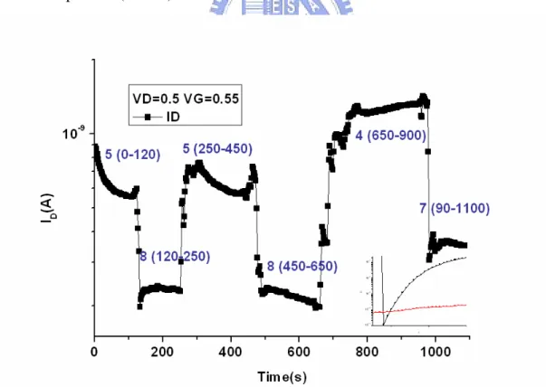
Figure 3-13 to Fig.3-15 show the sensing characteristics (ID-Time) for PBS (10mM) of
different pH. The test system is illustrated in Fig.3-16. As mentioned above, poly-Si materials
electrical characteristics. Fortunately, such concern could be lifted with the water passivation
effects [4]. As has been confirmed in this work, the electrical properties of the fabricated
NWFETs are stable in either air or water. As evidenced in Figure 3-6 and Fig. 3-7 and Fig. 3-8,
the characteristics of poly-Si NWFETs are improved and reproducible in the water-tasted
environment. One report describes that the fluid surrounding the nanowire sensor can
significantly affect the detection results with two factors. One is the electrostatics of the test
device due to the fringing-induced barrier. The other is the amount of charge induced on
nanowire.[10] For example, for the n-type channel devices tested in this work, negative
carries attached on the nanowire surface would affect the device’s threshold voltage.
Deionized water is usually slightly acidic because of the dissolved carbonic acid that it picks
up from the atmosphere. Therefore, deionized water will have a pH around 5 to 6 when
exposed to the air [11]. This chemical response is shown in below equation:
+ − + → → + H HCO CO H CO H O H CO 3 3 3 3 2 2 2
Moreover, the pKa (see appendix 2) of the silicon oxide is 6.8. Hence, the higher density of
charges presenting in the solution than in the air, we expect that the threshold voltage shift due
to the variation of the test solution should be more significant than in the air.
The silicon surface after wet handling that could produce the thickness between 0.6-2.0 nm
oxide-layer. Because of the silicon oxide possess the pKa =6.8. At high pH, -SiOH is
in Fig. 3-17. [12] To support this point, we carried out real-time pH-drain current
measurements on unmodified poly-Si NWFET. The results are shown in Fig. 3-13 to 3-14. To
test the reproducibility of the pH sensor, measurements under varied pH values were
repeatedly performed on a device. In addition we’ve also modified the poly-Si nanowire with
APTES(see in appendix 3), which produces amino groups, moreover, the amide group can
produce the other pKa(3.9).[13] Therefore, with the APTES treatment, we can extend the
measurements to solutions with a low pH value. The SiNW surface illustrating changes in the
surface charge state with pH is shown in Fig.3-18. [7] The data for modified poly-Si nanowire
are shown in Fig. 3-15. As expected [7] [8], the test devices with APTES-modified nanowire
surface show more steady performance than the unmodified one, especially while we
References:
[1]Okorn-Schmidt H.F.,1999. IBM J. res. develop. 43,351-365.
[2]Fossum ,J. Ortiz-Conde, G. A., 1983. IEEE Trans. Electron devices, 30,933-940.
[3]Baccarani,G., Ricco, B.,Shchini,G.,1978. J Appl. Phys.,49, 556-5570.
[4]Lin, H.C., Su, C.J., Huang, T.Y., 2007. Appl, phys, Letters,91.v 202113-1-202113-3.
[5] M. Shimaya, Proc. Int. Reliability Physics Symp., pp.292-296, 1995.
[6]Stern,E., Klemic,J. F., Routenberg, D. A., Wyrembak, P. N., Turner-Evans
D.B.,Hamilton ,A. D., LaVan, D. A. , Fahmy, T. M. & Reed ,M. A.,2007. Nature, 445.
519-522.
[7]Cui, Y., Wei, Q., Park, H., Lieber, C.M.,2001. Science, 293. 1289-1292.
[8]Chen,Y., Wang, X., Erramilli, S., Mohanty, P., 2006. Appl. Phys. Lett.,89.
223512-1-223512-3.
[9]Laws, G.M., Thornton, T.J., Yang, Garza, L.de la, Kozicki,M., Gust, D.,2002. Phys. Stat. sol.(b) 233. 83-89.
[10]Nair, P.R., Alam, A.,2007. IEEE Transactions on electron devices 54. 3400-3408.
[11] Leo M. L. Nollet (2000). Handbook of water analysis. (pp 70-71) CRC Press.
[12]Chua, L.L.,Zaumsell, J., Chang, J.F., Ou, E.C.-W., Ho, P.K.-H., Sirringhaus, H.,Friend, R.H.,2005. nature 434. 194-199.
[13] Vezenov, D. V., Noy, A., Rozsnyai, L. F., Lieber, C.M., 1997. J. Am. Chem. Soc.119. 2006-2015.
Figure 3- 1:Device A (a) Top and (b) cross-sectional views of the stacked dielectric oxide layer poly-Si NWFET .
Figure 3- 2:Device B (a) Top and (b) cross-sectional views of the stacked dielectric nitride and oxide layer poly-Si NWFET .
Figure 3- 3: (a) Top and (b) cross-sectional SEM images of poly-Si NWFET which NW channel as thin as 33-60nm wrapped by the spacer-wall.
Figure 3- 4:Device C (a) Top and (b) cross-sectional views of the stacked dielectric nitride layer poly-Si NWFET.
Figure 3- 5:The process steps for measurement of the electrical properties of the nanowire devices. 0.0 0.5 1.0 1.5 2.0 10-13 10-12 10-11 10-10 10-9 10-8 10-7 10-6 I D (A ) VG(V) VD=0.5V DRY1 WET2 DRY3 WET4 DRY5
Figure 3- 6:The electrical properties of the stacked dielectric oxide layer poly- Si NWFET (Device A) measuring in the air and water.
0.5 1.0 1.5 2.0 2.5 3.0 3.5 4.0 10-13 10-12 10-11 10-10 10-9 10-8 10-7 10-6 I D (A ) VG(V) VD=0.5V DRY1 WET2 DRY3 WET4 DRY5 WET6 DRY7
Figure 3- 7:The electrical properties of the stacked dielectric nitride and oxide layer poly-Si NWFET (Device B) measuring in the air and water.
0.0 0.5 1.0 1.5 10-14 10-13 10-12 10-11 10-10 10-9 10-8 10-7 10-6 10-5 VD=0.5V
DRY1 DRY2_after vacuum 30min
WET3 DRY4_after vacuum 1hr
WET5 DRY6_after vacuum 1hr
WET7
I D
(A
)
VG(V)
Figure 3- 8:The electrical properties of the stacked dielectric nitride layer poly-Si NWFET (Device C) measuring in the air and water.
-0.5 0.0 0.5 1.0 1.5 2.0 10-13 10-12 10-11 10-10 10-9 10-8 10-7 10-6 10-5 L=2um, VD=0.5V ID-2NW IG-2NW ID-4NW IG-4NW ID-6NW IG-6NW ID-10NW IG-10NW I D (A ) VG(V)
Figure 3- 9:Transfer characteristics of the proposed the stacked dielectric nitride layer poly-Si NWFET (device C) with difference channel that measures in the air.
0.0 0.5 1.0 1.5 2.0 10-13 10-12 10-11 10-10 10-9 10-8 10-7 10-6 2NW ,VD=0.5V ID-2um IG-2um ID-5um IG-5um ID-10um IG-10um I D (A ) VG(V)
Figure 3- 10:Transfer characteristics of the proposed the stacked dielectric nitride layer poly-Si NWFET (device C) with difference length that measures in the air.
-0.5 0.0 0.5 1.0 1.5 10-14 10-13 10-12 10-11 10-10 10-9 10-8 10-7 10-6 10-5 L=2um, VD=0.5V ID-2NW IG-2NW ID-4NW IG-4NW ID-6NW IG-6NW ID-10NW IG-10NW I D (A ) VG(V)
Figure 3- 11:Transfer characteristics of the proposed the stacked dielectric nitride layer poly-Si NWFET (device C) with difference length that measures in the water.
-0.5 0.0 0.5 1.0 1.5 10-13 10-12 10-11 10-10 10-9 10-8 10-7 10-6 2NW ,VD=0.5V ID-2um IG-2um ID-5um IG-5um ID-10um IG-10um I D (A ) VG(V)
Figure 3- 12:Transfer characteristics of the proposed the stacked dielectric nitride layer poly-Si NWFET (device C) with difference length that measures in the water.
Figure 3- 13:Real-time detection of the drain current for unmodified poly-Si nanowire for difference pH PBS(10mM).
Figure 3- 14:Real-time detection of the drain current for unmodified poly-Si nanowire for difference pH PBS (10mM).
0 200 400 600 800 1000 1200 1400 1600 10-8 6 5 7 7 8 7 2 4 5 3 6 4 3 2 -0.5 0.0 0.5 1.0 1.5 10-12 10-11 10-10 10-9 10-8 10-7 10-6 10-5 ID (A ) VG(V) ID IG I D (A) Time(s) VG=0.5V VD=0.5V pH
Figure 3- 15:Real-time detection of the drain current for APTES modified poly-Si nanowire for difference pH PBS(10mM).
Figure 3- 17:Schematics diagram of the interfacial charge trapping mechanism in which -SiOH is deprotonated to –SiO-. [10]
Figure 3- 18:Schematics diagram of the interfacial charge trapping mechanism. Zoom of the APTES-modified SiNW surface. [7]
2um 5um 10um 0.00 0.02 0.04 0.06 0.08 0.10 0.12 0.14 0.16 0.18 0.20 0.22 0.24 0.26 SS (V /de c ) Channel Length(um) 6NW without vacuuming with vacuuming
Table 3- 1:Summarizes the measured and extracted parameters of normalized on current from the device C (channel length = 2um, VG-Vth=0.7V, VD=0.5V).
Normalized
On Current NW¯2 NW¯4 NW¯6 NW¯10
Air 7.98E-8 2.78E-08 2.58E-08 2.55E-8
Water 3.08E-7 2.87E-7 2.81E-7 2.82E-7
Table 3- 2:Summarizes the measured and extracted parameters from the device C.
Channel length Vth(V) SS(V/dec) NW¯2 2um 5um 10um 0.5 0.35 0.37 0.16 0.16 0.15 NW¯4 2um 5um 10um 0.42 0.51 0.5 0.14 0.14 0.15 NW¯6 2um 5um 10um 0.52 0.36 0.29 0.14 0.14 0.24 NW¯10 2um 5um 10um 0.49 0.53 0.56 0.15 0.14 0.15
Chapter 4:Conclusion
In this thesis, we have successfully fabricated poly-Si NWFET with various numbers of
channels and various channel length. Well-behaved device characteristics are obtained in
either air or aqueous environment. Three types of NW devices formed on the surface of
different insulator were characterized. Among them, the split of device C which was formed
on the surface of a nitride capping was found to be most reliable and suitable for bio-logical
sensing application. This can be attributed to the high etch selectivity between nitride and the
other surface materials (e.g., nitride and oxide), so that the NW surface could be reliably
exposed to the environment with the wet etch treatment. In addition to exhibiting good device
characteristics in terms of lower threshold voltage and steeper subthreshold slope, clear water
passivation is also observed in the device C split.
We also demonstrated the effectiveness of the poly-Si NWFET used for pH-sensor
application. In this regard, we carried out real-time measurements to detect the difference in
pH PBS of the test solutions. The poly-Si NW devices are either modified or not with APTES.
The test devices with APTES-modified nanowire surface show more steady performance than
APPENDIX 1:The Protocol for Prepare 10mM PBS with Difference pH PBS.
Making a phosphate buffer solution is by phosphoric acid. Because of the phosphoric
acid has multiple dissociation constants, which are at 2.15, 6.86 and 12.32. The buffer is
most commonly prepared at pH 7 using monosodium phosphate and its conjugate base,
disodium phosphate.
1. Prepare the solution by mixing 10¯10-3 moles of monosodium phosphate and
10¯10-3 moles of disodium phosphate in a little less than a liter of water.
2. Then uniform-stir by hot plate with stirring bar.
3. Check the pH using a pH meter and adjust the pH as necessary using hydrochloric
acid or sodium hydroxide.
4. Once you have reached the desired pH, add water to bring the total volume of
phosphoric acid buffer to 1 L.
APPENDIX 2:Defined the Ka and pKa
Ka is called the acid-dissociation constant, and its value indicates the relative strength of
the acid. It is the equilibrium constant for a chemical reaction known as dissociation in the
context of acid-base reactions. For convenience, we will always write such reaction as shown
in below equation:
+ − +
⇔ A H
Moreover, the stronger the acid, the more it dissociates, giving a larger value of Ka.
Acid-dissociation constants vary over a wide range. Strong acids are almost completely
ionized in water, and their dissociation constants are greater than 1. The strength of acids is
usually expressed in terms of the pKa value:
a
a K
pK =−log
Because pKa is the negative logarithm of Ka, a numerically small value of pKa
corresponds to a strong acid, and a numerically large value to a weak acid. Some acids, such
the phosphoric acid, are capable of losing more than one proton. We called polyprotic acids.
The successive dissociation involve separate steps, with separate pKa values, hence, the PBS
exist in several different states of ionization, such as H3PO4 (phosphoric acid),
H2PO4-(dihydrogen phosphate ion), HPO42-(monohydrogen phosphate ion).
APPENDIX 3:The protocol of Modfied the poly-Si nanowire with APTES
1、Setup microfluidics apparatus for separated the water between the pad and the NW
channel that shown in Figure 2- 5.
2、For cleaning NW channel, apply the syringe to pump 0.3ml ethanol for three times.
3、Adding 2% ethanol solution of APTES by the syringe to pump the tube.
4、After waiting for 30 minutes, then cleaning by 0.3ml ethanol for three times.
minutes.
APPENDIX 4:The pKa of Silicon Nitride
Accurate values for the dissociation constants (pKa values) of the surface ionic groups on
silicon nitride are not available, but Auger and XPS studies indicate that there is a large
amount of oxygen bonded to silicon on the surface, indicating the presence of silylamine
(basic) and silanol (acidic) groups. Force measurements between silicon nitride surfaces
further indicate that the silylammonium groups become deprotonated (uncharged) at a pH of
8-10. Conclusive values for the dissociation constant of the silanol group are not available,
but the existence of a net neutral surface at pH 6-7 indicates that the pK of this group is below
6. (Chavez, P., Ducker, W., Israelachvili, J., and Maxwell, K., Langmuir 1996. 12,
簡歷 姓名:魏若芬 出生日期:民國七十二年十二月十五日 住址:新竹縣湖口鄉錦州一街九號 學歷: 國立竹北高中 資訊科 1999/9 - 2002/6 國立雲林科技大學 電子工程系 2002/9 - 2006/6 國立交通大學 生物醫學所 2006/9 - 2009/6 論文題目: 元件製程對於多晶矽奈米線場效電晶體水測電性影響之分析
Fabrication Process and its Effects on the Electric Characteristics of Poly Crystalline
![Table 1- 1 Comparison chart with various sensing methods. [21]](https://thumb-ap.123doks.com/thumbv2/9libinfo/8208798.169896/15.892.125.774.169.775/table-comparison-chart-various-sensing-methods.webp)