A
New
Grid-Generation Method for
2-D
Simulation
of Devices with Nonplanar Semiconductor Surface
Shan-Ping Chin, Student Member, IEEE, and Ching-Yuan W u , Member, IEEE
Abstract-A general analytical method is proposed to trans- form a 2-D multilayer physical domain with the nonplanar semiconductor surface into a 2-D rectangular mathematical do- main with the planar surface, in which a set of Fourier series are used to describe a general conformal mapping for each layer. Based on the proposed method, a simple iteration algo- rithm, which incorporates a nonlinear Jacobian-iteration method with the fast-Fourier transformation (FFT), is devel- oped to solve a system of nonlinear equations due to the mu- tually coupled boundary conditions. As a result of the analyti- cal conformal mapping, a regular, deformable grid-structure can be applied to simulate the device structure with the non- planar semiconductor surface, and the device simulator using the conventional rectangle-based grid can be easily modified to simulate the device with the nonplanar semiconductor surface.
I. INTRODUCTION
HE COMPLEXITY of device structure has been
T
raised due to the successive improvement of device- fabrication technology. The effects of the nonplanar semi- conductor surface can not be neglected for a modem scaled semiconductor device. Therefore, a device simu- lator with the capability of handling the nonplanar semi- conductor surface is necessary for the optimal design of a scaled semiconductor device.The basic grid-structure is very important for coding a device simulator in treating the nonplanar semiconductor surface. The triangle-based grid [l], [2] is the most widely used grid-structure in handling the nonplanar simulation domain. The major advantage of this method is its higher flexibility in locating the grid. However, this method re- quires more complicated codes and data structure due to the highly irregular grid-structure. Moreover, the obtuse triangle causes some problems and the efforts are needed to generate a triangular mesh without obtuse triangles.
Another approach for the grid-structure in nonplanar numerical simulation is the coordinate transformation method. This method has been widely used in other fields
131, 141 and is applied to control the quality of the grid- structure in semiconductor device simulation [ 5 ] , [ 6 ] . The basic procedure of this method is that several differential
Manuscript received March 9 , 1992; revised January 12, 1993. This work was supported by the National Science Council, Taiwan, Republic of China under Grant NSC-81-0404-E009-139. This paper was recommended by Associate Editor D. Scharfetter.
The authors are with the Advanced Semiconductor Device Research Lab- oratory and Institute of Electronics, National Chiao-Tung University, Hsinchu, Taiwan, Republic of China.
IEEE Log Number 9208516.
equations are described as the governing equations for co- ordinate transformation. A special case of coordinate transformation in 2-D simulation is that the 2-D Laplace equations are used as the governing equations. This is the well-known conformal mapping method and can be for- mulated by the Cauchy-Riemann relations. The single- layer numerical conformal mapping used in process sim- ulation has been developed in [7] for treating the moving
boundary problem. The major drawback of the numerical conformal mapping is that a set of 2-D Laplace equations must be solved self-consistently to satisfy the mutually coupled boundary conditions. As a result, a complicated numerical method is needed for solving these 2-D Laplace equations satisfying the mutually coupled boundary con- ditions.
In this paper, a simple analytical method for conformal mapping is developed, in which a set of Fourier series are used. Moreover, a curvilinear coordinate system is used to accurately describe the device structure and then is translated into the rectangular domain. The major features of this method are summarized as: 1) the regular grid structure is used to simulate the device with the nonplanar semiconductor surface; 2) the computational efforts for fitting the device structure are much reduced by adopting a nonlinear Jacobian-iteration method with the fast Fou- rier transformation (FFT), especially for a large number of Fourier series; 3) the discretized basic semiconductor
device equations are still valid under the proposed con- formal mapping.
In Section I1 the formulations of a general conformal mapping method are proposed and their physical pictures are discussed. In Section I11 a simple and efficient itera- tion algorithm is developed for solving a system of non- linear equations satisfying the mutually coupled boundary conditions. Section IV shows the actual generation of the grid structure for different isolation structures in a MOS-
FET and the detailed discussions on the nonlinear itera- tion are given. Section V gives a conclusion.
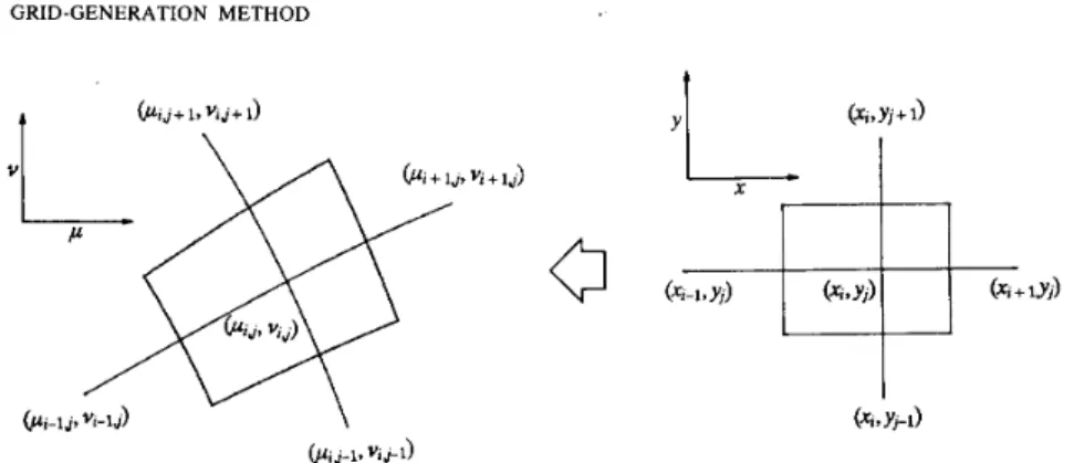
11. THE GENERAL CONFORMAL MAPPING METHOD As shown in Fig. 1, a set of semiconductor device equations have to be solved in a physical domain Q ( p , v). The conventional 2-D semiconductor device equations can be written as:
Fig. 1. The schematic cross-section of a semiconductor device with a non- planar structure. V
-
(-p,,nV*+
D,,Vn) = U,, - G,, V * (-pppV\k - DpVp) = Up - Gp. (2) (3) Among different grid structures, the rectangle-based grid is the most simple and widely used method in device simulation. Unfortunately, this grid-structure is limited in a rectangular-like physical domain. A transformation can be used to generalize the rectangular grid-structure to a nonplanar domain Cl. The transformation can be carried out by finding the functions pj(x, y) and uj(x, y) in each layer j . The partial differential operators under this trans- formation can be obtained as:a
axa
aya
aPj aPj
axaPj
aya
ax a
ay a
avj avj ax avj ay
+ - -
_ - - _ _
and
+
--. (4)Substituting (4) into (1) and ( 2 ) , the Poisson’s equation and the current continuity equation for electrons in the j-layer can be rewritten as
- - _ _ -
( 5 )
ax ay
ax ayaPj aPj
avj
auj
- _
+ - - = o
The constraint function (7a) is used to preserve the right angle between the lines in the transformation. For in- stance, the lines p (x, y) and v(x, y) for x = constant and y = constant constitute an orthogonal curvilinear coordi- nate system. Note that the comers in the simulation do- main are limited to the right angle by the constraint due to the right angle of the mathematical plane. The con- straint function (7b) means the conservation of the aspect ratio of an infinite small cell, i.e.,
J Y
As a result, the transformation produces the changes of position and size but keeps the angle and the aspect ratio under the constraints of (7a) and (7b). An example show- ing the transformation from a rectangular finite-box to a deformable finite-box under these constraints is plotted in Fig. 2. It is clearly seen that the orthogonality between the grid lines is preserved.
Although (7a) and (7b) are seen to be nonlinear, how- ever, the linearized forms of (7a) and (7b) can be ex- pressed as the well-known Cauchy-Riemann relations for the 2-D case:
From (9), we obtain
(9)
a 2 x a 2 x a 2 y
a 2 y
aPj
au;
aPj
av;
7
+
~ = 0 and 7+
~ = 0. (10)Note that the first and second terms in (5) and ( 6 ) become vanished if the 2-D Laplace equations in (10) are used.
( 4 9 Y,l)
&+ V ' t l )
Fig. 2. An example showing the mapping of a finite-box from the x - y (mathematical) plane onto the p-v (physical) plane
The relations in (9) are also true for their inverse func- tions:
apj avj
apj
avj
ax ay ay ax . ( 1 1)
From (7a), (7b), and (lo), the 2-D Poisson's equation and
the 2-D current continuity equations defined in the math-
ematical x - y plane can be rewritten as
- and - = - -
where J = [(ax/apj)2
+
( a y / a ~ ~ ) ~ ] - ~ . Note that (12) and (13) show a fact that the basic semiconductor equationsare invariant under the transformation satisfied by the Cauchy-Riemann relations. It is interesting to note that the discretized semiconductor device equations are not changed after the transformation from a rectangular do- main to a nonplanar domain if the transformation is con- formal. The invariability of the angle between the con- jugate grid lines and the aspect ratio of the finite box is very useful in modifying the codes used for simulating the planar device structure to those for simulating the non- planar device structure.
In order to find a set of the conjugate functions, p j ( x , y) and v j ( x , y), satisfied (11) in each layer, the equations
in (1 1 ) can be decoupled by mutual substitution, and the resulting equations can be written as a set of 2-D Laplace
equations:
a2pj a2pj
a2vj a 2 v .
ax2 +
7 = 0 and 7+
= 0. (14)JY ax ay
Although the 2-D Laplace equations in (14) form a set of
decoupled linear equations, it must be noted that the boundary conditions of these two Laplace equations are mutually coupled. As shown in Fig. 3, the numerical do-
main ( x - y) is mapped to the physical domain ( p - U), and the boundary conditions for (14) must satisfy the
V
i
Fig. 3 . An example showing the relation between the device structure and the mutually coupled boundary condition.
shape of the device structure in each layer, i.e.,
(15)
where j andjmax denote the j th interface and the total num- ber of the layer to be fitted, respectively.
The coupled boundary conditions in ( 1 5) describe the
nonlinear equations due to the shape of the semiconductor device and need a numerical algorithm to get the solution of (15). A numerical method for solving the above 2-D
partial differential equations with mutually coupled boundary conditions can be found in [7]. However, the numerical method for getting a conformal mapping needs much computational efforts due to a large linear system with mutually coupled boundary conditions. The problem for doing this coordinate transformation analytically is how to get a set of general solutions for (11). Our ap-
(bj - Y + Y j ) - Bj,m si& k m ( Y - ~ j ) l . ( 16b) Note that the conjugate functions, p j ( x , y ) and v j ( x , y ) in (16), are the particular solutions of the 2-D Laplace equa- tions in (14), respectively. The coefficients, Aj,
,
and Bj, ,, have to be solved by satisfying mutually coupled bound- ary conditions (15).Substituting (16a) and (16b) into (15), the following equations can be obtained for y = y j and y = y j
+
bj:m
(x
+
zl
sin (krnx) [Ai,, coth (kmbj)+
Bj,,
csch ( k , bj)] m = -c
Aj., cos (k,x), ( 1 7 4 m = I 03 J ; + 1 (x+
c
sin (k,x) [A,,, csch (k,bj) m = 1 + Bj,m ~ 0 t h (krnbjll m = bj+
C
Bj,, cos (k,x). ( 17b) m = ITransforming (17a) and (17b) into cosine-Fourier series, the following equations are obtained:
f. J 9 m = - A . J , m , f o r m = 1, 2, 3 ,
-
3 00 (18a) (18b) (18c) where$,, and$ + l , m are the Fourier coefficients of$( p ( x ,y j ) ) and
fi
+ ( p (x, y j+
bj)) , respectively, and can be ex- pressed as: = Bj,,, f o r m = 1, 2, 3 , * * * 7 03 bj =$ +
I , O - $ , o c = 1 f o r m = 0; c = 2 form # 0 (19a) f j + l , r n =5
L o S L $ ( p ( x 7 Yj+
bj)) cos (kmx) h, c = 1 f o r m = 0; c = 2 form # 0. (19b)B,. These coefficients must be determined from the known device structure. The computation efficiency and accu- racy for solving (18a)-(18c) are determined by two fac- tors: one is the number of Fourier series; the other is the numerical method and its convergence criterion in the nonlinear iteration. The FFT method is used to perform the Fourier transformation, in which the number of Fou- rier series can be expressed as n = 2*, where p is a pos- itive integer. The major advantage of the FFT algorithm is that CPU time for a FFT transformation is O ( n X log (n)). This feature is very important for accurately mod- eling the device structure with a large number of Fourier series.
Among the solution methods for a system of nonlinear equations, the Newton’s method is the best known pro- cedure. In general, the Newton’s method is expected to give quadratic convergence, provided that a sufficiently accurate initial guess is needed. However, the Newton’s method needs to construct a Jacobian matrix and its in- version. The CPU time for calculating the coefficient in the Jacobian matrix for the nonlinear system (18a)-( 18c) is O ( n X n X log ( n ) ) by using a FFT algorithm. As a result, the efficiency of the Newton’s method will degrade seriously when the problem size is large. This limits the Newton’s method to the case with only a small number of unknown variables. Thus, a nonlinear Jacobian-iteration is adopted to solve the system of nonlinear equations, which is more favorable than the Newton’s method for a large problem size because the Jacobian matrix is not nec- essary for the proposed nonlinear Jacobian-iteration scheme. However, the major drawback of the nonlinear Jacobian iteration is that the coupling effect between the variables is not well considered and the convergence of the nonlinear Jacobian iteration is strongly dependent on the property of the equations.
The algorithm for solving the coefficients Aj,
,
and Bj,,
with w as a relaxation parameter is listed as follows: Procedure Fourier-Conformal-Mapping
Initialize Ai,,, Bj,,, and bj
For k = 1, kmaxdo
p = l
Calculate pf(x, yj) and pf(x, yj
+
6,) by FFT Calculate f; (x) andfF+
(x)Translate
ff
(x) andfj”+
(x) To ff,,
and f f + I ,,by FFT
$ + I = f F + 1 , 0
-fro
F o r m = 1, 2 p do
= A;, - w(fFkrn
+
A;,,) = ~ : , m+
W ( f j + l , r n - Bim)Fig. 4. The grid structures for different isolation structures: (a) LOCOS
structure, and (b) Trench-like structure.
End for
If (convergence criterion is reached) then Initialize A j , , = 0, B j , , = 0 for m Calculate increasing residue
If (increasing residue less than one half of p = p + 1
= 2 p - '
+
1 t o 2 Pconvergence criterion) stop End if
End for
End Fourier-Conformal-Mapping
where the symbol k denotes the kth iteration; n denotes the number of Fourier series, which is equal to 2p. In this algorithm, two FFT procedures are needed for each Ja- cobian iteration. Note that the convergence criterion must be properly chosen to avoid the generation of the ripple- like grids.
Generally, the convergence of Fourier series is O(e-") for C" function. This property is useful for the contin- uation method in solving A , and B,. The solutions for the problem with the 2 p terms of Fourier series are used as the initial guess for the problem with the 2p +
'
terms ofFourier series. As the residue of the iteration for the prob- lem with the 2 p terms of Fourier series reaches to a certain criterion, p is increased by 1. The p is increased until the truncation error of Fourier series meets the requirement of the desired accuracy. In this algorithm, the maximum number of p is determined by the increased residue less than one half of the convergence criterion when p is in- creased by 1. According to the convergence of Fourier
series ( O ( e - " ) ) , the truncation error of Fourier series is expected to be around the residue of nonlinear iteration.
Once the coefficients A , and B, are determined by the numerical algorithm, the grid points in each node (i ', j
'
) can be determined byOD sin (k,x,.,,) " ' , J ' = x"J
+ c
,
= 1 sinh (k,b,)* [Ai,, cosh krn(b1 - Y J , + YJ) + Bj,m
cosh km ( Y J , - (20a)
and
O1 COS (krnxi,,j) = yJn - y, -
c
m = I sinh (k, b,)
[A,,, sinh km (bj - ~ j+ , Y,) - B 1 . m sinh km ( ~ j- ,
~j)1.
Note that the coefficients A , and B, are different for each subdomain and the x-grid lines in each mathematical sub- domain must be determined to meet the continuity of p-grid lines across the interface between the subdomain.
IV. RESULTS AND DISCUSSIONS
In this section, some practical examples showing the applications of the proposed Fourier conformal mapping algorithm are demonstrated and discussed in detail. The generated grid structures for comparing the narrow-width effect between different isolation structures: LOCOS and
1
0 1 2 3 4
Gate Width Cum)
Fig. 5 . Comparisons of the threshold voltage versus the effective gate width for different isolation structures of a MOSFET.
Trench-like are shown in Fig. 4(a) and (b), respectively, in which one half of the grids are used in the simulation due to the symmetry of the device structure. It must be noted that the orthogonality of the finite-box is kept, as shown in Fig. 4(a) and (b). The isolation structures are basically formed by two regions (layers): the semicon-
ductor bulk and the insulator layer, in which the semicon- ductor bulk is covered by the insulator layer and the in- sulator layer has a transition region between field oxide and gate oxide. The hypertangent function can be used to describe these transitions. For a LOCOS structure, the shape functions forfo ( p ) ,
fi
( p ) , and& ( p ) can be approx- imated by: fo(p) = -0.2425+
0.2125 tanh ~ ( pLY)
f i ( p ) = 0.2125 - 0.2125 tanh ~ ( p;.Y)
&(CL) = 3. (2 1 c)Similarly, for a Trench-like structure, we may write:
fi
( p ) = 0.375 - 0.375 t a d ~(
cco.?)
& ( A
= 3. (22c)The thicknesses of gate oxideo and field oxide for these structures are 300 and 8500 A , respectively. Note that the nonplanarity of the Trench-like structure is stronger than that of the LOCOS structure. The calculated thresh- old voltage versus the effective gatewidth for different iso- lation structures is shown in Fig. 5. It is clearly seen that the narrow-width effect in a Trench-like isolation struc- ture is superior to that in a LOCOS isolation structure.
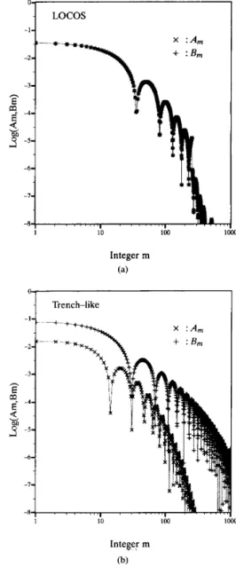
The coefficients of Fourier series ( A , and B,) versus integer m used in the transformation for the oxide region
M
5
-5- -6- -7- 1 10 Integer m (a) 0 - 8 , , , , , , , , , I , , , , , , ,-
1 10 1w Integer m (b) K1Fig. 6 . The logarithmic plot of Fourier coefficients ( A m , B,) versus integer rn for the transformation of the oxide region: (a) LOCOS structure and (b)
Trench-like structure.
of LOCOS and Trench-like structures are shown in Fig. 6(a) and (b). A , is equal to B,,, for the LOCOS structure due to the symmetry of the shape functions
fo(
p ) andfi
( p ) . Note that the convergence of Fourier series is O ( e - " ) . It is clearly shown in Fig. 6(a) and (b) that the magnitude and convergence of the Fourier series are strongly dependent on the nonplanarity of the semicon- ductor surface. It is expected that more Fourier series terms must be used to minimize the truncation error for Fourier series with slow convergence. In order to meet the same convergence criterion, the number of Fourier se- ries for the Trench-like isolation are larger than that for the LOCOS isolation due to the slow convergence ofg
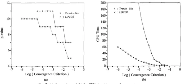
1205
100.-
6
80i
Log ( Convergence Criterion ) Log ( Convergence Criterion )
(a) (b)
Fig. 7. (a) the p value and (b) the CPU time (s) versus the convergence
criterion (Run by IBM RS/6000 model 320 workstation).
Fourier series for a Trench-like structure, as shown in Fig. 7(a). Besides, the convergence rate of the proposed non- linear Jacobian iteration is dependent on the nonplanarity of the semiconductor surface. As a result, the CPU-time versus the convergence criterion for the transformation of the Trench-like structure is larger than that of the LOCOS structure, as shown in Fig. 7(b). Therefore, the compu- tation efficiency will be deteriorated for the case with a strongly nonplanar semiconductor surface due to the slow convergence rate of both nonlinear Jacobian iteration and Fourier series.
The shape functions in (21)-(23) are only used to dem- onstrate the applications of the proposed method. Ac- tually, the polynomial fitting method or other appropriate special function can be used to increase the accuracy of the shape function for the actual device structure.
V . CONCLUSIONS
A general analytical method to generate the grid struc- ture for the nonplanar semiconductor surface is presented, in which the analytical formulation and the numerical al- gorithm are described in detail. The major advantage of the proposed method is that the discretized semiconductor device equations are invariant under the proposed coor- dinate transformation. It is demonstrated that the pro- posed method is efficient for the smooth semiconductor surface with mild nonplanarities, but the efficiency be- comes deteriorated for the case with a strongly nonplanar semiconductor surface. Therefore, the proposed method is useful in improving the flexibility of conventional rec- tangular-based grid in handling the modem isolation de- vice structures, such as modified LOCOS and Trench-like technologies.
ACKNOWLEDGMENT
Special thanks are given to Ms. G . 4 . Hou for her help-
ful discussions.
REFERENCES
[ l ] M. R. Pinto, C . S . Rafferty, and R. W. Dutton, “PISCES-I1 Poisson
and continuity equation solver, ” Stanford Electronics Labs. Rep.,
Stanford Univ., CA, 1984.
[2] G . Baccarani, R. Guemeri, P. Ciampolini, and M. Rudan, ‘“FIELDS:
A highly-flexible 2-D semiconductor devices analysis program,” in
Proc. NASECODE IV Conf., pp. 3-12, 1985.
[3] A. M. Winslow, “Numerical solution of the quasilinear Poisson’s equation in a nonuniform triangle mesh,” J . Compur. Phys., vol. 2,
pp. 149-172, 1967.
[4] J . U. Brackbill and J . S . Saltzman, “Adaptive zoning for singular
problems in two dimensions,” J . Compur. Phys., vol. 46, pp. 342-
368, 1982.
[5] Z. M. V.-Kovacs and M. Rudan, “Boundary fitted coordinate gener- ation for device analysis on composite and complicated geometries,”
IEEE Trans. Computer-Aided Design, vol. 10, pp. 1242-1250, 1991.
[6] P. Ciampolini, A. Forghieri, A. Pierantoni, A. Gnudi, M. V. Rudan,
and G . Baccarani, “Adaptive mesh generation preserving the quality
of the initial grid,” IEEE Trans. Computer-Aided Design, vol. 8, pp.
490-500, 1989.
[7] A. Seidl and M . Svoboda, “Numerical conformal mapping for treat-
ment of geometry problems in process simulation, ’’ IEEE Trans. Elec-
tron Devices, vol. ED-32, pp. 1960-1963, 1985.
Shan-Ping Chin (S’86) received the B.S. degree from the Department of Physics, National Tsing- Hua University, Taiwan, Republic of China, in 1985, and the Ph.D. degree from the institute of
Electronics, National Chiao-Tung University, in 1992.
His research interests are in the device model- ing of deep submicrometer MESFET’s. He joined the Electronics Research and Service Organiza- tion (ERSO), ITRI, Taiwan, in 1992. His present interests focus on semiconductor device and IC
process simulation for VLSI
Ching-Yuan Wu (M’72) received the B.S. degree
in electrical engineering from National Taiwan University, Taiwan, Republic of China, in 1968, and the M.S. and Ph.D. degrees from the State University of New York (SUNY) at Stony Brook, in 1970 and 1972, respectively.
During the 1972-1973 academic year he was appointed as a Lecturer at the Department of Elec- trical Sciences, SUNY, Stony Brook. During the 1973-1975 academic years, he was a Visiting As- sociate Professor at National Chiao-Tung Univer-
zation (ERSO), ITRI; a member of the Academic Review Committee, the Ministry of Education; and the chairman of the Technical Review Com- mittee on Information and Microelectronics Technologies, the Ministry of Economic Affairs. His research activities have been in semiconductor de- vice physics and modelings, integrated-circuit designs and technologies.
the Chinese Educational and Cultural Foundation, in 1985. He has received the outstanding research Professor fellowship from the Ministry of Edu- cation and the National Science Council (NSC), Republic of China, during