Chang Pin Huang and Chih Chena)
Department of Material Science and Engineering, National Chiao Tung University, Hsinchu 30050, Taiwan, Republic of China
C.Y. Liu
Department of Chemical Engineering and Materials Engineering, National Central University, Chung-Li, Taiwan, Republic of China
S.S. Lin and K.H. Chen
Megic Corporation, Ltd., Hsin-chu 300, Taiwan, Republic of China (Received 1 June 2005; accepted 6 July 2005)
Nickel has been widely used as an under-bump metallization (UBM) material in the microelectronics industry. The solid-state reaction between the eutectic SnAg solder bumps and three thicknesses of Ni/Cu UBM was investigated, with 5m-Cu/3 m-Ni, 3m-Cu/2 m-Ni, and 0 m-Cu/1 m-Ni. It was found that the shear strength of the solder bumps decreased after the solid-state aging at 150 °C for 200 h, and it did not change much after it was prolonged for 500 and 1000 h. Aging of the Ag3Sn intermetallic compound (IMC) and grain growth of the solder are responsible for the decrease in the shear strength. Furthermore, the shear test results indicated that the fracture mode switched from ductile to brittle for the solder bumps with 1m Ni after aging longer than 200 h, causing the strength of the solder to decrease abruptly. This is attributed to the consumption of the peripheral Ni layer after the solid-state aging for 1000 h. The Ni consumption rate was measured to be 0.02m/h1/2at 150 °C.
I. INTRODUCTION
Flip-chip technology has been adopted in high-performance electronics devices because a large number of tiny solder bumps can be fabricated into an area array on a chip as input/output (I/O) interconnections.1 Pb-containing solder has been used for over 30 years to form flip-chip joints, reacting with under bump metallurgy (UBM).2,3However with increasing environmental con-cerns, the microelectronics industry is paying greater at-tention to lead-free solder alternatives.4,5One of the most promising alternatives is SnAg3.5 solder for flip chip packages, and manufacturing. SnAg3.5 solder bumps on a wafer by electrical plating or printing technology is now commercially available. Therefore, it can be imple-mented in fine-pitch solder joints.
The metallurgical reactions between the Pb-containing solders and different UBMs have been studied exten-sively over the past decade. Copper and nickel are the two common UBM materials used in the packaging in-dustry. Copper reacts with the solder alloy very quickly
and provides excellent wetting.6Yet, for thin Cu film, the fast consumption rate of the Cu UBM may cause spalling of the interfacial intermetallic compound (IMC) after longer reflowing time.7 Therefore, Ni UBM has been also used due to its lower reaction rate with the solder alloy.8Due to its high stress, the Ni film cannot be de-posited too thickly. Thus, the combination of the Cu and Ni films was adopted in the packaging industry, and sev-eral approaches were studied, including Al/Ni(V)/Cu,9 co-sputtering Cu-Ni alloy,10,11 and electroplated Cu/Ni films.12
With the implementation of Pb-free solder, spalling also occurs in the Pb-free solder jointed to the Al/Ni(V)/ Cu UBM.13
Electroplated Cu/Ni appears to be a prom-ising UBM for the Pb-free solders because of the low-cost process, in which the Ni layer serves as a wetting layer, and the Cu film serves as a stress buffer layer. Several studies have addressed the metallurgical reaction of Pb-free solders and the Ni UBM.14,15 However, the thickness effect of the Cu/Ni film on the metallurgical reaction has not been studied, and the minimum thick-ness of the Ni layer required is still unknown. In this paper, we examine the interfacial reaction of the SnAg solder bump with three different thicknesses of the Cu/Ni film, with 5/3m, 3/2 m, and 0/1 m. Shear tests were
a)
Address all correspondence to this author. e-mail: [email protected]
performed to investigate the bump strength after various solid-state aging times. This study provides deeper un-derstanding of the thickness effect of the Cu/Ni film and the UBM with SnAg solder.
II. EXPERIMENTAL
Schematics of the three samples used in this study are shown in Figs. 1(a)–1(c). Titanium of 0.1 m of was sputtered onto the oxidized Si wafer and acts as an ad-hesion layer. Copper of 0.5m was then sputtered onto the Ti layer and served as a seed layer for the subsequent electroplating process. Then the Cu or Ni layer was elec-troplated on the Ti/Cu layers. Photolithography was applied to define the opening for solder electroplating. Afterwards, the UBM opening was formed by a wet-etching process. Due to the fast wet-etching rate of Cu, the diameter of the Cu UBM was smaller than that of the Ni
UBM, as shown in Figs. 1(a) and 1(b). There was no electroplated Cu layer in the third sample. The Ni film served as a wetting/reaction layer. Then the eutectic SnAg solder was electroplated onto the film. The solder bumps were formed by reflowing in an infrared oven at 260 °C for about 1 min. In this paper, the three samples in Figs. 1(a)–1(c) were denoted as 5 m-Cu/3 m-Ni, 3m-Cu/2 m-Ni, and 0 m-Cu/1 m-Ni, respectively. For metallurgical reaction at solid-state reactions, samples were aged at 0, 200, 500, and 1000 h at 150 °C in nitrogen atmosphere. The cooling rate was kept con-stant about 5 °C/s for all the samples because it can change the Ag3Sn morphology.
16
The mean height and diameter of solder balls were 95.5 and 142 m after a reflow. The shear strength of solder bumps was measured by a shearing arm at the speed of 100m/s and height of 15m. The shear strength was obtained by averaging the results from 50 solder bumps in each test condition on the same wafer. Thickness and morphology of the interfacial IMC layer were determined from the cross-sectional ob-servation. A solution of nitric acid, acetic acid, and glyc-erin at the ratio of 1:1:1 was used for the selective etching of Sn. The morphology and composition of IMC were examined by using a JEOL 6500 field-emission scanning electron microscope (SEM) and energy dispersive spec-troscopy (EDS).
III. RESULTS AND DISCUSSION
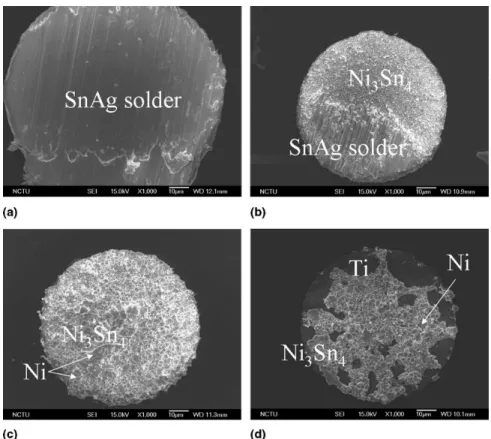
The microstructures of the as-fabricated solder bumps for the three samples are shown in Figs. 2(a)–2(c). There were no clear differences in the microstructure of the solder and in the interfacial IMCs. Figures 2(d)–2(f) show the corresponding enlarged SEM images at the interface of the SnAg solder and the Ni layer. An inter-metallic compound of Ni3Sn4was detected at the inter-face. Significant variations in shear strength were ob-served for the three samples at various aging times, as shown in Fig. 3. The shear strength decreased as the aging time increased, and it decreased abruptly after ag-ing for 200 h. For the 5m-Cu/3 m-Ni and 3 m-Cu/ 2 m-Ni samples, it decreased sharply from 56.5 to 47.4 MPa, which is a 16.1% reduction. It was almost constant after further aging up to 1000 h. In particular, the shear strength for the 0 m-Cu/1 m-Ni sample dropped from 55.1 to 43.7 MPa after aging for 200 h, which is a 20.7% reduction. The shear strength dropped lower than 44.0 MPa, which is typical specification. It continued to decrease down to 41.0 after aging for 1000 h. The fracture surfaces were inspected by SEM and EDS. Figures 4(a)–4(d) show the four typical fracture surfaces in this study, including ductile facture in the solder, partial brittle facture in the solder and IMC/Ni interface, brittle facture in the IMC/Ni interface, and brittle facture in the IMC/Ti interface. For the 5m-Cu/ FIG. 1. Schematic illustrations for the three types of SnAg solder
bumps used in this study: (a) 5 m-Cu/3 m-Ni, (b) 3 m-Cu/2 m-Ni, and (c) 0 m-Cu/1 m-Ni.
3 m-Ni and 3 m-Cu/2 m-Ni samples, the fracture occurred inside solder bumps for all solid state reactions, as shown in Fig. 4(a). The fracture surface of the 0 m-Cu/1m-Ni sample varied with aging condition. With-out the thermal aging, fracture occurred inside the solder bumps. However, the fracture switched to partial brittle mode for approximate 40% of the bumps, as shown in Fig. 4(b). The intermetallic compound of Ni3Sn4 was detected on the fracture surface in these cases. After fur-ther aging to 500 h, most of the fracture surfaces be-came brittle mode, while both Ni and Ni3Sn4 IMC re-gions can be detected on the fracture surfaces, as shown in Fig. 4(c). With longer aging up to 1000 h, the fracture surface occurred mainly at the IMC/Ni interface, as
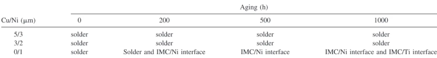
shown in Fig. 4(c). The fracture of a few samples oc-curred at the IMC/Ti interface, as illustrated in Fig. 4(d). Titanium, nickel, and Ni3Sn4IMC layers were found on the fracture surface, as indicated by arrows in Fig. 4. This indicated that the 1-m Ni layer and the 0.5-m sput-tered Cu layer might be partially consumed after thermal aging of 1000 h. The fracture modes for the three types of the samples are summarized in Table I.
The reduction in shear strength with the increase in aging time in SnAg-based solders has also been reported by other researchers.17–19Coarsening of Ag3Sn was pro-posed to be responsible for the reduction of strength since the fine dispersive Ag3Sn IMC may strengthen the solder by precipitation hardening. On the other hand, the solder FIG. 2. Cross-sectional SEM images for the SnAg solder bumps: (a) 5m-Cu/3 m-Ni sample, (b) 3 m-Cu/2 m-Ni sample, (c) 0 m-Cu/1 m-Ni samples, (d) magnified image for the interfacial structure in (a), (e) magnified image for the interfacial structure in (b), and (f) magnified image for the interfacial structure in (c).
grains may also grow during the solid-state aging, caus-ing the decrease in the shear strength. Figures 5(a)–5(d) show the typical SEM images of the Sn3.5Ag solder bumps after the aging for 0, 200, 500, and 1000 h, re-spectively. The solder grains can be observed clearly. The average grain size of the solder was about 3.3 m before the thermal aging, as shown in Fig. 5(a), and it grew to 15.2 m after the aging for 200 h of all the samples, as observed in Figs. 5(b)–5(d). The driving force of the grain size growth was decreased grain
boundary area.20,21The grain size remained almost con-stant after 200 h of aging. In addition, the spherical Ag3Sn precipitation could be observed, as indicated in the Figs. 5(a)–5(d).16The fine Ag3Sn precipitations dis-tributed in the grain boundary of the solder before ther-mal aging, and significant ripening took place after 200 h of aging. The size of the Ag3Sn IMC did not increase noticeably after aging for 200 h. Because the fracture occurred in the solder bumps for 5m-Cu/3 m-Ni and 3m-Cu/2 m-Ni samples, the coarsening of the Ag3Sn IMC and the grain growth of the solder may be respon-sible for the abrupt drop in the shear strength after 200 h of aging. Furthermore, the grain size and the size of the Ag3Sn IMC remained almost unchanged after 200 h of aging, and the shear strength stayed almost constant for the two samples after 200 h of aging.
The decrease in the shear strength may be attributed to the grain growth of the solder and the coarsening of Ag3Sn precipitation. For the former, the yield strength (y) decreased with the increase of the grain size.
22 The Hall–Petch equation related the yield strength (y) to the grain size (d) below the equicohesive temperature (ECT)
y⳱ 0+d −1/2
, (1)
whereyis yield strength,0is Peierls stress (resistance of crystal), is Hall–Petch slope, and d is mean grain
FIG. 4. Four typical fracture modes after shear test in this study: (a) ductile facture in the solder, (b) partial brittle facture in the IMC/Ni interface, (c) brittle facture in the IMC/Ni interface, and (d) brittle facture in the IMC/Ti interface.
FIG. 3. Shear test results for the three types of SnAg solder bumps at different aging times up to 1000 h. The shear strength of the 0 m-Cu/1m-Ni samples dropped below the specification of 44 MPa after 200 h aging.
size. For the later, the Lifshitz–Slezov–Wagner (LSW) theory describes the time evolution of Ag3Sn grown dur-ing thermal agdur-ing times.23
In this study, the size of the Ag3Sn is 0.1–0.6m after a reflow, and it grew to 0.6– 3.1m in all samples after thermal aging for 200 h. This coarsening of the Ag3Sn is a ripening phenomenon. The driving force of the Ag3Sn growth was to minimize the total interfacial surface area between the Ag3Sn and the solder, which is a ripening phenomenon. With further aging to 1000 h, the grain sizes of the Ag3Sn did not change much. The Ag3Sn precipitates inside the solder ball produced Orowan’s mechanism of dispersion strengthening.24The Orowan’s mechanism of dispersion strengthening can be described by Eq. (2)
⳱ Gb/l , (2)
where is shear strength, G is shear modulus, b is Burg-ers vector, and l is the distance between two second phase particles. If precipitation volumes are constant, the
precipitations are smaller, numerous, circular, discon-tinuous, and with better shear strength. The shear strength decreased because of the Ag3Sn and the maxi-mum diameter (l) increased during thermal aging.
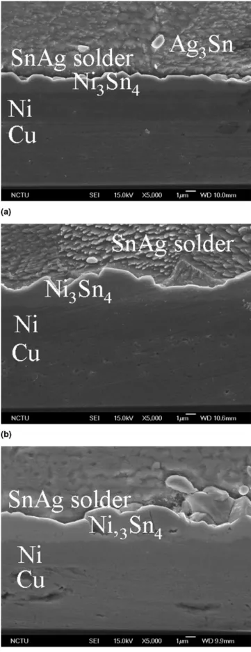
To investigate the unique failure mechanism for the 0m-Cu/1 m-Ni samples, the interfacial structure be-tween the solder and the UBM was examined by scan-ning electron microscopy (SEM). Figures 6(a)–6(c) show the cross-sectional SEM images of the interfacial struc-ture for the 5 m-Cu/3 m-Ni samples after the 200, 500, and 1000 h aging, respectively. The Ni3Sn4 layer grew thicker as the aging time increased, and its compo-sition remained almost unchanged during the aging proc-ess. The interfacial microstructure for the 3 m-Cu/2 Ni samples was quite similar to that of the 5 m-Cu/3 m-Ni samples except that the remaining Ni was thinner. Figures 7(a)–7(c) show the interfacial structure for the 0m-Cu/1 m-Ni samples, and the Ni3Sn4layer was also detected.
FIG. 5. SEM images showing the grain size of the SnAg solder after (a) 0 h, (b) 200 h, (c) 500 h, and (d) 1000 h thermal aging. TABLE I. Fracture modes for the three types of samples at various aging times.
Cu/Ni (m)
Aging (h)
0 200 500 1000
5/3 solder solder solder solder
3/2 solder solder solder solder
FIG. 6. Cross-sectional SEM images of the 5m-Cu/3 m-Ni sample after (a) 200 h, (b) 500 h, and (c) 1000 h thermal aging.
FIG. 7. Cross-sectional SEM images of the 0 m-Cu/1 m-Ni samples after (a) 200 h, (b) 500 h, and (c) 1000 h thermal aging. Complete consumption of the Ni UBM was observed occasionally, as indicated by the arrow in the (c).
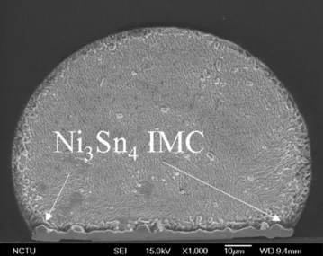
However, depletion of the 1-m Ni layer was found at some locations after the aging for 1000 h, as indicated by the arrows in Fig. 7(c). Therefore, the Ni layer became discontinuous. Since Cu atoms diffused much faster than the Ni atoms and they tend to dissolve into the Ni3Sn4 IMC, the sputtered Cu layer may be consumed quickly, which would deteriorate the adhesion of the interface because of the high interfacial energy between the IMC and the Ti film. The depletion of Ni may be responsible for the brittle facture mode in the IMC/adhesion inter-face, as shown in Fig. 4(d). Yet, it was not clear how the partial brittle facture and the brittle facture in the IMC/Ni interface happened after the 200 and 500 h aging for the 0m-Cu/1 m-Ni samples since there were no obvious differences in the microstructure and the composition for the interfacial IMC among the three types of samples. One possible reason for this usual fracture mode is the side-attack of the Ni UBM. Figure 8 shows the cross-sectional SEM image of the 0m-Cu/1 m-Ni samples after 1000 h aging, and it is found that the periphery of the Ni UBM was consumed completely and formed Ni3Sn4 IMC. This side-attack may result in two conse-quences for the shear test. First, the periphery may have higher stress concentration and become a weak point. During the shear test, a crack may initiate there and propagate along the IMC/UBM interface, causing the partially brittle fracture and the brittle fracture in the IMC/Ni interface. Secondly, once the Ni/Cu in the pe-riphery of the UBM was consumed completely, the ef-fective adhesion area was reduced accordingly. Com-pared with Figs. 2(a)–2(c), the diameter of the UBM with Ni/Cu layer shrank after the side-attack, which results in the decrease in the shear stress for the 0m-Cu/1 m-Ni samples after aging.
FIG. 8. Cross-sectional SEM image of the 0m-Cu/1 m-Ni samples after 1000 h aging, showing that the periphery of the Ni UBM was consumed completely and formed Ni3Sn4IMC
FIG. 9. (a) Thickness of the Ni3Sn4IMC as a function of the aging
time, (b) thickness of the Ni3Sn4IMC as a function of the square root
of the aging time, and (c) Ni UBM consumption as a function of the square root of the aging time for the three types of the SnAg solder bumps.
The consumption rate of the electroplated Ni during aging was measured. Figure 9(a) shows the thickness of the Ni3Sn4IMC as a function of aging time for the three types of the samples. It can be seen to increase with the increase of aging time. Figure 9(b) illustrates the plot of the IMC thickness with the square root of the aging time, and it shows a diffusion-controlled behavior in the IMC growth. The slope was linear according to Fick’s second law
X⳱ (kt)1/2 , (3)
where X is interfacial Ni3Sn4 thickness, k is the rate constant, and t is aging time. The slope is square root of the rate constant (k1/2), and the value is 0.075m/h1/2at 150 °C. In addition, the consumption of Ni in thickness was also calculated, as depicted in Fig. 9(c). It shows that it takes about 1870.6 h to consume the 1-m Ni layer. However, due to the non-uniformity of the thickness dur-ing the electroplatdur-ing process, the Ni thickness may in some areas be thinner than 1m, which may cause local depletion of the Ni layer.
IV. CONCLUSIONS
The solid-state reaction between the eutectic SnAg solder bumps and three various thicknesses of Ni/Cu UBM has been investigated. It is found that ripening of the Ag3Sn intermetallic IMC and grain growth of the solder are responsible for the decrease in the shear strength after aging at 150 °C for 200 h. Solder bumps with 5m-Cu/3 m-Ni and 3 m-Cu/2 m-Ni showed no obvious deterioration after the thermal aging up to 1000 h. However, for 0 m-Cu/1 m-Ni samples, the shear strength dropped below the specification after ag-ing for 200 h. The partial consumption of the 1 m Ni layer after aging for 1000 h may be responsible for the sharp decrease in the shear strength.
ACKNOWLEDGMENT
The authors would like to thank the National Science Council of Taiwan, Republic of China, for financial sup-port through Grant No. 92-2216-E-009-008.
REFERENCES
1. J.H. Lau: Flip Chip Technology (McGraw-Hill, New York, 1995), Chap. 3, p. 123.
2. L.F. Miller: Controlled collapse reflow chip jointing. IBM J. Res. Develop. 13(3), 239 (1969).
3. P.A. Totta and R.P. Sopher: SLT device metallurgy and its mono-lithic extension. IBM J. Res. Develop. 13(3), 226 (1969). 4. D. Suraski and K. Seelig: The current status of lead-free solder
alloys. IEEE Trans. Electron. Pack. Manuf., 24, 244 (2001). 5. K.N. Tu and K. Zeng: Sn-Pb solder reaction in flip chip
technol-ogy. Mater. Sci. Eng. Rep. R 34, 1 (2001).
6. H.K. Kim and K.N. Tu: Rate of consumption of Cu soldering accompanied by ripening. Appl. Phys. Lett. 67, 2002 (1995). 7. A.A. Liu, H.K. Kim, K.N. Tu, and P.A. Totta: Palling of Cu6Sn5
spheroids in the soldering reaction of eutectic SnPb on Cr/Cu/Au thin films. J. Appl. Phys. 80, 2774 (1996).
8. P.G. Kim, J.W. Jang, T.Y. Lee, and K.N. Tu: Interfacial reaction and wetting behavior in eutectic SnPb solder on Ni/Ti thin films and Ni foils. J. Appl. Phys. 86, 6746 (1999).
9. C.Y. Liu, K.N. Tu, T.T. Sheng, C.H. Tung, D.R. Frear, and P. Elenius: Electron microscopy study of interfacial reaction be-tween eutectic SnPb and Cu/Ni(V)/Al thin film metallization. J. Appl. Phys. 87, 750 (2000).
10. S.H. Kim, J.Y. Kim, J. Yu, and T.Y. Lee: Residual stress and in-terfacial reaction of the electroplated Ni-Cu alloy under bump metallurgy in the flip-chip solder joint. J. Electron. Mater. 33, 948 (2004).
11. T.M. Korhonen, P. Su, S.J. Hong, M.A. Korhonen, and C.Y. Li: Reactions of lead-free solders with CuNi metallizations. J. Elec-tron. Mater. 29, 1194 (2000).
12. L.L. Duan, D.Q. Yu, S.Q. Han, J. Zhao, and L. Wang: Microstruc-ture and interface reaction between Sn-3.5Ag solder and electro-plated Ni layer on Cu substrate during high temperature exposure, in Business of Electronic Product Reliability and Liability, 2004 International Conference on Apr 27–30, (IEEE, Shanghai, China, 2004), pp. 35–41.
13. K. Zeng and K.N. Tu: Six cases of reliability study of Pb-free solder joints in electronic packaging technology. Mater. Sci. Eng. R 38, 55 (2002).
14. Y.C. Chan, P.L. Tu, C.W. Tang, K.C. Hung, and J.K.L. Lai: Re-liability studies ofBGA solder joints-effect of Ni–Sn interme-tallic compound. IEEE Trans. Adv. Pack. 24, 25 (2001). 15. C.S. Huang, J.G. Duh, and Y.M. Chen: Metallurgical reaction of
the Sn–3.5Ag solder and Sn–37Pb solder with Ni/Cu under-bump metallization in a flip-chip package. J. Electron. Mater. 32, 1509 (2003).
16. F. Ochoa, J.J. Williams, and N. Chawla: Effects of cooling rate on the microstructure and tensile behavior of a Sn–3.5 wt% Ag sol-der. J. Electron. Mater. 32, 1414 (2003).
17. H.T. Lee, M.H. Chen, H.M. Jao, and C.J. Hsu: Effect of adding Sb on microstructure and adhesive strength of Sn–Ag solder joint. J. Electron. Mater. 33, 1048 (2004).
18. A. Sharif, M.N. Islam, and C.Y. Chan: Interfacial reactions of BGA Sn–3.5% Ag–0.5% Cu and Sn–3.5% Ag solder during high-temperature aging with Ni/Au metallization. Mater. Sci. Eng. B 113,184 (2004).
19. C.T. Peng, C.T. Kuo, and K.N. Chiang: Experimental character-ization and mechanical behavior analysis on intermetallic com-pounds of 96.5Sn–3.5Ag and 63Sn–37Pb solder bump with Ti–Cu–Ni UBM on copper chip, in Electronic Components and Technology Conference, (IEEE, Las Vegas, NV, 2004), Vol. 1, pp. 90–97.
20. A.M. Gusak and K.N. Tu: Theory of normal grain growth in nor-malized size space. Acta Mater. 51, 3895 (2003).
21. R.E. Reed-Hill and R. Abbaschian: Physical Metallurgy Prin-ciples, 3rd ed. (Florida Univ. Press, PWS Publishing Company, Boston, MA, 1994), pp. 185, 251.
22. R.E. Reed-Hill and R. Abbaschian: Physical Metallurgy Prin-ciples, 3rd ed. (PWS Publishing Company, Boston, MA, 1994), p. 193.
23. A.M. Gusak and K.N. Tu: Kinetic theory of flux-driven ripening. Phys. Rev. B 66, 115403 (2002).
24. R.E. Reed-Hill and R. Abbaschian: Physical Metallurgy Prin-ciples, 3rd ed. (PWS Publishing company, Boston, MA, 1994), pp. 118, 120, 532.