Pergamon
Solid-State Electronics Vol. 39, No. 7, pp. 1005-1009, 1996 Copyright 0 1996 Elsevier Science Ltd 0038~1101(95)00415-7 Printed in Great Britain. All rights reserved 0038-1101/96 $15.00+0.00
ENHANCEMENT
OF THE OPTICAL AND ELECTRICAL
PROPERTIES
IN InGaAlP/InGaP
PIN
HETEROSTRUCTURES
BY RAPID THERMAL
ANNEALING
ON MISORIENTED
SUBSTRATE
A. CHIN, H. Y. LIN and B. C. LIN
Department of Electronics Engineering, National Chiao Tung University, Hsinchu, Taiwan, Republic of China
(Received 16 August 1995; in revised form 20 October 1995)
Abstract-We have studied the optical and electrical properties of InGaAlP/InGaP PIN heterostructures by the effects of post-growth annealing, substrate misorientation and growth temperature. For the as-grown p-type It~,,~(Cia&l~,,)~,,P, the 15” misoriented sample shows the largest hole concentration of 1 x 10” crn3
as compared to 2” and 10” misoriented samples. After annealing at 900°C for 30 s, the hole concentration increases about three times to 2.6 x 10’s cme3. The increased hole concentration is related to the four times enhanced photoluminescence (PL) intensity. In the II~~.~G~~,~P/I~,,(G~,,A~,),,P stained multiple quantum wells, the post-growth annealing also improves the PL integrated intensity. The PL intensity on an as-grown sample decreases with the increased degree of misorientation, while the PL peak energy increases with the increased degree of misorientation, from o”, 2”, 10” toward 15”. The PL intensities are larger for samples grown at 760°C than those grown at 700°C. Copyright 0 1996 Elsevier Science Ltd
1. INTRODUCTION
InGaAlP alloys have attracted much attention and been studied extensively, because of the growth induced ordering and compositional modulation effect [l-4] and their application in opto-electronic devices in the visible wavelength region[5-81. These materials have direct band-gaps that cover the red to green wavelength region, with a lattice matched to GaAs. Therefore these materials are one of the best candi- dates for high brightness light emitting diodes (LEDs) in this wavelength region. However, the performance of a InGaAlP laser diode (LD) or LED is strongly related to the growth condition, such as residual moisture, growth temperature, V/III ratio, and growth rate[2]. Furthermore, the achievement of low p-type resistivity in InGaAlP becomes more difficult as Al composition is increased[9]. The measured hole con- centration is strongly dependent on the substrate mis- orientation and growth conditions[lO-121. A similar difficulty of achieving high P-type doping activity and efficiency is also observed in other large bandgap materials, such as GaN[13] and ZnSe[l4]. The other difficulty of InGaAlP is the high Al composition related deep levels and non-radiative recombination centers[5,15] which reduce the emission efficiency and increase the threshold current density of LDs. Unfortunately, a high Al composition is required for shorter emission wavelength and for use as barriers for LEDs and LDs. Therefore, it is very important to improve both doping activity and the material quality of InGaAlP in order to reduce the series resistance
of the device and increase the emission efficiency. Recently, the application of post-growth annealing to activate p-type dopants in wide bandgap GaN material has been reported[l3]. After annealing at temperatures above 7OO”C, the conductivity increases several orders of magnitude. The improved electrical property was attributed to the reduced deep-level emissions, as shown by an order of magnitude en- hanced photoluminescence (PL) intensity. By similar post-growth heat treatment, the improved activation of Zn acceptors in InGaAlP has also been reported [16]. However, there is no detailed comparison of the optical properties in InGaAlP after heat treatment, and the non-radiative recombination in InGaAlP barrier is important to the performance of LEDs and LDs.
In this paper we have studied the post-growth annealing effects and substrate misorientation on the optical and electrical properties of InGaAlP/ InGaP PIN heterostructures. For Zn-doped In,,,(Ga,,A~,,),,P, post-growth annealing improves the hole concentration by a factor of two to three, and the largest hole concentration of 2.6 x 1Ou cme3 was obtained from the 15” misoriented sample. The improved electrical property after annealing is believed to be due to the increased doping activation efficiency. In the I~,~Ga,,~P/I~,,(Ga,,Al,,),,P strained multiple quantum wells active region, the post-growth anneal- ing also improves the PL integrated intensity. These strained quantum wells are quite stable after anneal- ing at 925°C for 30 s. Substrate misorientation and growth temperature effects can also improve the PL
1006 A. Chin et al,
integrated intensity. The PL intensity is larger for the sample grown at a higher temperature of 760°C than for the sample grown at 700°C. The PL intensity increases monotonically as the degree of misorienta- tion is decreased, while the peak energy is generally increased with the increased degree of misorientation.
2. EXPERIMENT
The samples studied were grown by a low pressure metalorganic vapor phase epitaxy (MOVPE) reactor, with horizontal infrared heating and a gas flow rotation. A more detailed growth can be found else- where[lO]. Substrate temperatures of 700 and 760°C were chosen for layers grown on misoriented (100) GaAs substrates tilted towards (11 l)A. Zn-doped, 1 pm thick In,,(G~,,Al,,),,,P layers were grown at 700°C on undoped 2”, 10” and 15” misoriented (100) GaAs, in order to study the effect of substrate mis- orientation and post-growth annealing on the optical and electrical properties. The large degree of mis- orientation used here is to improve the Zn doping efficiency as reported by Kondo et af.[17]. The anneal- ing conditions are at temperatures ranging from 800 to 925”C, for 30 s, and in a nitrogen atmosphere. Samples were proximity capped with a GaAs substrate in order to avoid the desorption of arsenic and phosphorus. We also studied the post-growth annealing effect on misoriented In,,,Ga,,dP strained multiple quantum wells PIN heterostructure. The layer structure consists of a thin Si-doped n + GaAs buffer, 0.75 pm Si-doped n 1r1,,~(Ga,,Al,,),,,P bottom barrier, 0.1 pm undoped In,,,(Ga,,,Al,,),,P bottom spacer, undoped active layer, 0.1 pm undoped In,., (Gq., Al,,,),,, P top spacer, 0.75 pm Zn-doped p In,,,(Ga,,,Al,,),,P top barrier, 0.1 pm Zn-doped p+ In,,,Ga,,,P and 0.2pm Zn- doped p+ GaAs contact layer. The active region contains three periods of 70 8, InO,,Gq,dP strained quantum well and 150 8, In,, 5 (Gao.6Al,.,),,, P barrier. This is a typical structure for red LDs. Both Zn doped GaAs and InGaP layers were etched away before PL measurement. The PL was measured at - 10 K using an Ar+-ion laser (488 nm) as the excitation source, and the signal was detected with a cooled photo- multiplier. All the measurements were done under identical conditions in order to compare the relative PL intensities. Hall measurement was used to charac- terize the electrical properties of the epitaxial layers.
3. RESULTS AND DISCUSSION
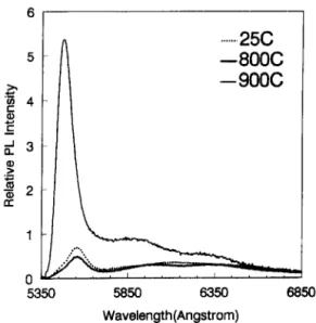
Figure 1 shows the low temperature PL spectra of as-grown and annealed samples of Zn-doped,
6 >. .z 4 5 I iI!3
s
‘G m 22
. . . 25c
-800C
- 9ooc
.%m
5650 6350 Wavelength(Angstrom) 6650Fig. 1. Low temperature (10°K) PL spectra of as-grown and annealed 2” misoriented, Zn-doped Ino,s(G~~SAl,,,)O,,P. The annealed conditions were 800 and 900°C for 30 s. The
excitation intensity was at 10 W cm-2.
2” misoriented In,,(G~,,Al,,),,P. The annealing temperatures are 800 and 900°C for 30 s. A large full width at half maximum (FWHM) linewidth of 56 meV for the as-grown sample is related to impurity broad- ening effects, and such linewidth is typical for epitaxial layers at a high hole concentration of 7 x 1017cm-3. There is little change in the PL spectrum after 8OO“C annealing. In contrast, there is a four times enhanced PL integrated intensity after 900°C annealing. The enhancement of the PL integrated intensity is related to the reduced non-radiative recombination centers[l3] and the increased doping activity[l3,16] after anneal- ing. The increased luminescence efficiency is very important to improve the light emission intensity and achieve the low threshold current density of LDs. It is also observed that the peak energies increase from 2.231 eV to 2.263 eV, for the as-grown and 900°C annealed layers, respectively. It was reported that alloy ordering and bandgap narrowing exist in this material and Zn diffusion can disorder the InGaP[4]. Therefore the 32 meV increase of the PL peak energy after annealing may be due to the similar disordering effect of Zn diffusion during the thermal cycle.
The electrical properties of misoriented, and Zn- doped I~.s(Ga,,Al,,),,P epitaxial layers were further evaluated by Hall measurements. The measured Hall data are summarized in Table 1. For the as-grown p-type samples, the 15” misoriented one shows the largest hole concentration of 1 x lO’*cm-’ as
Table I. Measured room temperature Hall data for 1.0 pm thick annealed and misoriented (100) Ino.5 (%., AL )a.~ P
Mobility (cm’, V-’ SK’) Carrier density (cm-‘)
Miscut As-grown 800°C 900°C As-grown 800°C 900°C
2” (100) 9 IO 8 7.0 x IO” 5.7 x IO” 1.4 x 10’8
IO” (100) 47 26 29 3.4 x 10” 1.0 x IO’S 1.0 x 10’8
lnGaAlP/lnGaP PIN heterostructures 1007
5c
-0 degree
. . . ...2degree
-10 degree
-15 degree
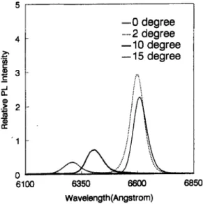
6350 6600 Wavelength(Angstrom)Fig. 2. Low temperature (10°K) PL spectra of as-grown ln,,Gaa,P strained multiple quantum wells PIN hetero- structure grown at 700°C on o”, 2”, IO” and 15” misoriented
GaAs. The excitation intensity was at 10 W crne2.
compared to the 2” and lo” misoriented samples. Hole concentrations are larger for the 900°C annealed samples than that for the as-grown layers. This is also consistent with the enhanced PL integrated intensity after 900°C annealing. The annealing effect at 900°C for 30 s, can increase the carrier concentration by two to three times that of the as-grown one, regardless of the degree of misorientation. The largest hole concentration of 2.6 x 101*ctn3 was obtained from the annealed 15” misoriented sample. The increased hole concentration after post-growth annealing is very important to reduce the series resistance and the turn-on voltage for large band-gap p-type materials. Although the detailed mechanism of increased hole
5 4 .$ 53 E i: .z 2 -m t? ‘1 0 6100
-0 degree
...,2
degree
- 10 degree
- 15 degree
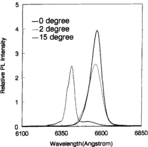
6350 6600 Wavelength(Angstrom) 6650Fig. 3. Low temperature (10°K) PL spectra of annealed l%,,Ga,,,P strained multiple quantum wells PIN hetero-
structure grown at 700°C on 0”, 2”, 10” and 15” misoriented GaAs. The excitation intensity was at 10 W cme2.
concentration after annealing is not fully understood, it is believed to be due to the decreased effects of hydrogen passivation on the acceptors[ 16,181 and decreased concentration of deep levels[ 19.
The successful improvement of both the apical and electrical properties of %-doped ln,,~(G~,,Al,,),,,P was applied to the lnGaP/lnGaAlP multiple quantum wells PIN heterostructures. Figure 2 shows the as- grown PL spectra of ln,,,Ga,,,P multiple quantum wells grown at 700°C. The PL peak energy increases monotonically from 1.872, 1.878, 1.937, to 1.967 eV for the O”, 2”, 10” and 15” misoriented samples, re- spectively. The 95 meV PL peak energy shift between the 0” and 15” misoriented samples is related to the ordering effect[l9]. Under similar measurement con- ditions, the PL integrated intensity decreases mono- tonically with an increased degree of misorientation. The relative PL integrated intensities are 2.8, 2.6, 1 .O and 1.0 for the 0”, 2”, 10” and 15” misoriented samples, respectively. We have chosen the lowest PL integrated intensity of 700°C grown and 15” mis- oriented sample as 1 .O. The 0” on-axis sample shows the largest PL intensity and is -three times larger than that of the 15” misoriented one. Similar ordering related PL peak energy red shift and PL integrated intensity enhancement were also observed in ordered (11 l)B AlGaAs[ZO].
Figure 3 shows the PL spectra for post-growth annealed 700°C grown In,,hGa,,P multiple quantum wells. The annealing condition is 925°C for 30 s. After annealing, the PL peak energies are 1.876, 1.879, 1.934 and 1.965 eV for the 0”, 2”, 10” and 15” misoriented samples, respectively. The change of PL peak energy, by only few meV after annealing indicates the good thermal stability in the InGaP quantum well region. However, after annealing, the PL integrated intensities are increased to 3.5, 4.7, 1.5 and 1.1 for the oi’, 2”, lo” and 15” misoriented samples, respectively. The increased PL integrated intensity, with only few meV shifts of PL peak energy, indicates that the thermal annealing effect can reduce the deep-level related non-radiative recombination centers. A similar anneal- ing effect was also observed in GaN[ 131. The improved PL integrated intensity after annealing is important to the device performance of LD. The reduced non- radiative recombination centers can enhance the luminescence efficiency and therefore reduce the threshold current of LD.
We have also studied the annealing effect on 760°C grown ln,,~G~,~P multiple quantum wells. Figures 4 and 5 show the as-grown and post-growth annealed PL spectra, respectively, for the ln,,,Gar,4P multiple quantum wells grown at 760°C. In order to compare the annealing effect on different growth temperatures, we have summarized the PL peak energy and relative PL integrated intensity in Tables 2 and 3, respectively. We have chosen the relative value of the lowest PL integrated intensity as 1.0. In spite of the increase in growth temperature from 700 to 760°C the 15” mis- oriented sample still shows the highest PL peak energy,
1008 A. Chin et al.
-0 degree
...2
degree
-15 degree
6100 6350 6600 6850 Viavelength(Angstrom)Fig. 4. Low temperature (10°K) PL spectra of as-grown III,,~GQ,,P strained multiple quantum wells PIN hetero- structure grown at 760°C on 0”, 2” and IS” misoriented
GaAs. The excitation intensity was at 10 W cme2.
r
-0 degree
6100 6350 6600
Wavelength(Angstrom)
6850
Fig. 5. Low temperature (10°K) PL spectra of annealed In,,,Ga,,P strained multiple quantum wells PIN hetero- structure grown at 760°C on o”, 2” and 15” misoriented
GaAs. The excitation intensity was at 10 W cmd2.
as compared to that of the 0” and 2” misorientations. However, the difference between the highest and lowest PL peak energy is reduced from 95 to 37 meV, for the 700 and 760°C grown samples, respectively. This is due to the high growth temperature induced disordering effect[l9]. A similar high growth tempera- ture induced disordering effect has also been observed in AlGaAs[ZO].
Another important factor for laser diode perform- ance is the PL integrated intensity. The PL integrated intensity is larger for samples grown at 760°C than for those grown at 700°C. The increased PL integrated intensity with growth temperature is due to the reduced concentration of defect related non-radiative
Table 2. PL peak energies for as-grown and post-growth annealed
samples. The annealing condition is 925°C for 30 s As-grown Post-growth annealed 700°C 7wc 700°C 760°C Mismt growth growth growth growth
0” (100) I.872 1.891 i ,876 1.888
2” (100) 1.878 1.890 1.879 1.891 10’ (100) 1.937 1.934 -
15” ilooj 1.967 I .928 I.965 I .934
Table 3. Relative PL integrated intensity for as-grown and post- growth annealed samples. The annealing condition is 925°C for 30 s
Miscut 0” (100) 2” (loo) lo” (100) 15” (100) As-grown 700°C 760°C growth growth 2.8 6.1 2.6 4.3 1.0 - 1.0 3.4 Post-growth annealed 700°C 7wc growth growth 3.5 7.8 4.7 6.0 1.5 - I.1 3.8
recombination centers. This is expected from the higher surface migration velocity of adatoms and the lower oxygen incorporation at the higher growth temperature. It is shown in Table 3 that the post- growth annealing effect increases the relative PL inte- grated intensity, regardless of the growth temperature and substrate misorientation. The improvement of PL integrated intensity after annealing indicates that the concentration of non-radiative recombination centers is reduced in the quantum wells and barriers. Another ordering and compositional modulation related phenomenon is the monotonically decreasing PL integrated intensity with increasing degree of misorientation. The 15” misoriented sample has the lowest PL integrated intensity and the highest PL peak energy, while the 0” misoriented sample has the highest PL integrated intensity and the lowest PL peak energy. The long range ordering in InGaP modifies the In and Ga composition and forms In rich domains[21]. Such In rich domains lower the PL peak energy and increase the PL integrated intensity. A similar PL integrated intensity enhancement and red shift of PL peak energy, reported in AlGaAs, are also attributed to the growth related spontaneous ordering and compositional modulation[20].
4. CONCLUSIONS
We have shown that a nearly three times enhanced hole concentration can be achieved after annealing for P-type In,.,(Ga,,Al,,),,P, and the largest hole concentration of 2.6 x lo’* cme3 was obtained from the 15” misoriented sample. The improved four times PL integrated intensity, after post-growth annealing, is believed to be due to the increased doping activity and also due to reduced non-radiative recombination centers. We also studied the annealing effect on the strained In,,sGaO,P multiple quantum wells grown on misoriented substrates. These strained quantum wells are quite stable after annealing at 925°C for 30 s, as observed from the few meV changes of PL peak energy. The relative PL integrated intensity is also
InGaAIP/InGaP PIN heterostructures 1009
increased after annealing. The reduced non-radiative A. S. H. Liao, Appl. Phys. Left. 61, 1045 (1992). recombination and series resistance after annealing 9. Y. Nishikawa, Y. Tsuburai, C. Nozaki, Y. Ohba and are very important to the performance of LDs and IO. J.-F. Lin. M.-J. Jou. C.-Y. Chen and B.-J. Lee, Y. Kokubun, Appl. Phys. Left. 53, 2182 (1988).
LEDs. J. Crystal Growth 124, 415 (1992).
11. A. Valster, C. T. H. F. Liedenbaum, M. N. Finke, Acknowledgements-We would like to thank M. J. Jou, and A. L. G. Sevems, M. J. B. Boermans, D. E. W. B. J. Lee at Opto-Electronics & Systems Labs., ITRI, for Vandenhoudt and C. .W. T. Bulle-Lieuwma, J. Crystal providing the material. The work has been supported by NSC Growth 107, 403 (1991).
(83-0417-E-009-017, and 83-0404-E-009-097) in Taiwan. 12. K. Kadoiwa, M. Kato, T. Motoda, T. Ishida, N. Fujii, N. Hayafuji, M. Tsugami, T. Sonoda, S. Takamiya and
I. 2. 3. 4. 5. 6. 7. 8. REFERENCES
G. S. Chen, T. Y. Wang and G. B. Stringfellow, Appl.
Phys. Left. 56, 1463 (1990). _.
L. C. Su. I. H. Ho and G. B. Strinafellow. J. Ad. Phvs.
75, 5135 (1994). ._ .
S. Yasuami, C. Nozaki and Y. Ohba, Appl. Phys. L&r. 52, 2031 (1988).
A. Gomyo, T. Suzuki, K. Kobayashi, S. Kawata and I. Hino, Appl. Phys. Len. SO, 673 (1987).
H. Sugawara, K. Itaya, H. Nozaki and G. Hatakoshi, Appl. Phys. L&r. 61, 1775 (1992).
M. Mannoh, J. Hoshina, S. Kamiyama, H. Ohta, Y. Ban and K. Ohnaka, Appl. Phys. Lat. 62, 1173 (1993).
C. P. Kuo, R. M. Fletcher, T. D. Osentowski, M. C. Lardizabal, M. G. Craford and V. M. Robbins, Appl. Phys. Lerr. 57, 2937 (1990).
Jpn. .I. Appl. ihys. 31, Li39 (1992).
14. R. M. Park, M. B. Troffer, C. M. Rouleau, J. M. DePuydt and M. A. Haase, Appl. Phys. Len. 57, 2127 (1990).
15. S. Nojima, H. Tanaka and H. Asahi, J. Appl. Phys. 59, 3489 (1986).
16. H. Hamada, S. Honda, M. Shono, R. Hiroyama, K. Yodoshi and T. Yamaguchi, Electron. Lerr. 28, 585 (1992).
17. M. Kondo, C. Anayama, T. Tanahashi and S. Yamazaki, J. Crystal Growth 124, 449 (1992).
18. A. Kamata, H. Mitsuhashi and H. Fujita, Appl. Phys. L-err. 63, 3353 (1993).
19. J. E. Fouquet, M. S. Minsky and S. J. Rosner, Appl. Phys.-Lat. 63, 3212 (199j).
20. A. Chin. H. Y. Lin and K. Y. Hsieh. J. Crvsrd Growrh 150,438 (1995).
K. H. Huang, J. G. Yu, C. P. Kuo, R. M. Fletcher, 21. 0. Ueda, M. Takechi and J. Komeno, Appl. Phys. Len. T. D. Osentowski, L. J. Stinson, M. G. Craford and 54, 2312 (1989).
S. Mitsui;J. CrysraiGrowrh 145, 147 (1994). 13. S. Nakamura. T. Mukai. M. Senoh and N. Iwasa,