High Reliability Ultrathin Interpolyoxynitride Dielectrics
Prepared by N
2O Plasma Annealing
Jer Chyi Wang,aJam Wem Lee,bLiang Tai Kuo,aTan Fu Lei,a,z
and Chung Len Leea
aDepartment of Electronics Engineering, National Chiao-Tung University, Hsinchu 300, Taiwan b
National Nano Device Laboratories, Hsinchu 300, Taiwan
This work addresses the preparation of ultrathin共effective oxide thickness, 42 Å兲 interpoly-oxynitride (SiOxNy) films by annealing thin nitride films with high density N2O plasma and N2O rapid thermal annealing. The proposed oxynitride dielectrics formed using N2O plasma annealing exhibited low gate leakage current, high breakdown electric field, long ten-year lifetime, and large effective barrier height. These superior properties can be attributed to the high concentration of oxygen incorporated in the poly-II/nitride interface and a reduction of the trap density of the interpoly-oxynitride films. The dielectric is a suitable substitute for the inter-polyoxide of electrically-erasable programmable read only memory.
© 2003 The Electrochemical Society. 关DOI: 10.1149/1.1619993兴 All rights reserved. Manuscript received July 15, 2002. Available electronically October 9, 2003.
Deep submicrometer electrically-erasable programmable read only memory共EEPROM兲 requires a thin polyoxide with a low leak-age current, a high breakdown field (Ebd), a large charge to break-down (Qbd), and a low electron trapping rate to ensure good data retention and endurance characteristics.1-4 Oxide/nitride/oxide 共ONO兲 multilayered films have been extensively investigated and frequently used as the dielectric layer in the flash memory devices and other applications.5-7 However, the scaling down of the inter-poly dielectrics is critical for next generation nonvolatile memories with a small cell size and low programming voltage. Recently, many studies8-11 were successfully employed tetra-ethyl-ortho-silicate 共TEOS兲 vapor deposited polyoxide with rapid-thermal-annealing 共RTA兲 with N2O10or NH3 pretreatment,11increasing reliability by making the interface smoother after oxidation. Unfortunately, the quality of thermally oxidized and TEOS vapor-deposited polyoxide is strongly related to the surface roughness and doping concentration of poly I. This relationship raises issues of reliability and scaling limits of the interpoly oxide.12
Oxynitride films have attracted much attention as gate and tunnel dielectrics for submicrometer devices due to their superior proper-ties and better reliability than the conventional silicon dioxide films.13,14A previous study15 of nitrided oxides demonstrated ad-vanced properties owing to the presence of nitrogen at the interface. Moreover, the fact that oxynitride has a higher dielectric constant than the silicon dioxide presents many opportunities to decrease the equivalent oxide thickness共EOT兲. Not only metal oxide semicon-ductor field effect transistors but also electrically erasable and pro-grammable read only memory共EEPROMs兲 depend on scaling of the thickness of the oxide to exhibit a large driving capability and charge storage. This work proposes, for the first time, an ultrathin interpoly-oxynitride (EOT⫽ 42 Å) deposited by low pressure chemical vapor deposition共LPCVD兲 with high density N2O plasma annealing. The fabricated interpoly-oxynitride has a very long ten-year lifetime, a low electron trapping rate, a high breakdown electric field, and a high barrier height. The interpoly-oxynitride, when used in EEPROM applications, can improve performance and reliability.
Experimental
The n⫹-polysilicon/polyoxide/n⫹-polysilicon capacitors were fabricated on p-type silicon共100兲 wafers. First, silicon wafers were thermally oxidized at 900°C to form a 20 nm thick isolation oxide. Then a 300 nm polysilicon layer 共poly-I兲 was deposited in an LPCVD system using SiH4 gas at 620°C and subsequently doped with POCl3at 850°C for 40 min and drive-in for 20 min, resulting in a sheet resistance of 30-40⍀/䊐. After the stripping off of p-glass
and standard RCA cleaning, the Si3N4films, 40 Å and 50 Å thick, were deposited in an LPCVD system at 650°C followed with a N2O-plasma annealing 共PLA兲 at 50 W for 5 min and N2O-RTA annealing at 950°C for 30 s. Thereafter, a second 300 nm polysilicon layer共poly-II兲 was deposited by an LPCVD system at 620°C and doped to a sheet resistance of 30-40⍀/䊐 by the same POCl3process as that for poly-I. After definition of the poly-II, all samples were covered with a 300 nm oxide as a passivation layer by plasma en-hanced chemical vapor deposition. Contact holes were opened and aluminum was deposited and patterned to form final capacitor struc-tures. Finally, all devices were sintered at 400°C for 30 min in an N2 ambient. A cross-sectional view of the interpoly-oxynitride dielec-trics is shown in Fig. 1.
The EOT of the interpoly-oxynitride was determined by the high frequency共100 kHz兲 capacitance-voltage 共C-V兲 in the strong accu-mulation region using a Keithley 590 and 595. Moreover, the physi-cal thickness was estimated by transmission electron microscopy 共TEM兲. The electrical properties and reliabilities were measured us-ing an HP 4156B semiconductor parameter analyzer.
Results and Discussion
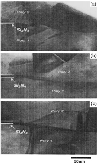
Figure 2a, b, and c show the TEM images of a 50 Å interpoly-nitride film of the control sample共without annealing兲 and the oxyni-tride dielectrics with RTN2O annealed at 950°C for 30 s and N2O plasma annealed at 50 W for 5 min, respectively. A small increment in the interpoly-oxynitride thickness was observed after RTN2O or N2O plasma annealing. The annealing can oxidize the nitride films to form oxynitride dielectrics; meanwhile, the oxygen atoms may be incorporated in the nitride/polysilicon interface by various annealing methods, improving the reliability characteristics of the interpoly-oxynitride dielectrics. Additionally, from the TEM picture of the
zE-mail: [email protected]
Figure 1. Cross-sectional view of the ultrathin interpolysilicon-oxynitride
interpoly-oxynitride sample with N2O plasma annealing shown in Fig. 2c, the thickness can be estimated to be 80 Å, and the dielectric constant of the oxynitride was nearly 6.24, which value can be de-rived from the electrical thickness of 49 Å obtained from the high frequency C-V characteristics. Figure 3a shows the positive current-density potential 共J-E兲 characteristics of the ultrathin interpoly-nitride film of the control sample共As兲 and the interpoly-oxynitride
dielectrics with RTN2O annealed at 950°C for 30s共RTA兲 and N2O plasma annealed at 50 W for 5 min共PLA兲. The characteristics of all samples with similar EOTs, between 42 and 43 Å, were compared. The RTA sample exhibited the lowest leakage current owing to the local improvement of the nitride/poly-I interface by the RTN2O an-nealing. RTN2O annealing has been reported to suppress the leakage current of CVD nitride films by forming an interfacial oxide at the nitride/silicon interface.16Consequently, for the interpoly-nitride di-electric with RTN2O annealing, an Si3N4/SiOxNystructure may be formed by incorporating the high concentration of oxygen at the nitride/poly-I interface. The fact that the electron barrier of SiOxNy films is higher than that of Si3N4dielectrics may be responsible for the low leakage current. The negative J-E characteristics shown in Fig. 3b, on the contrary, the interpoly-oxynitride dielectric annealed by the N2O plasma has the lowest leakage current. This result indi-cates that annealing effects of the N2O plasma on the interpoly-oxynitride dielectrics are superior to those of RTN2O, due to the incorporation of a high concentration of oxygen at the poly-II/nitride interface.
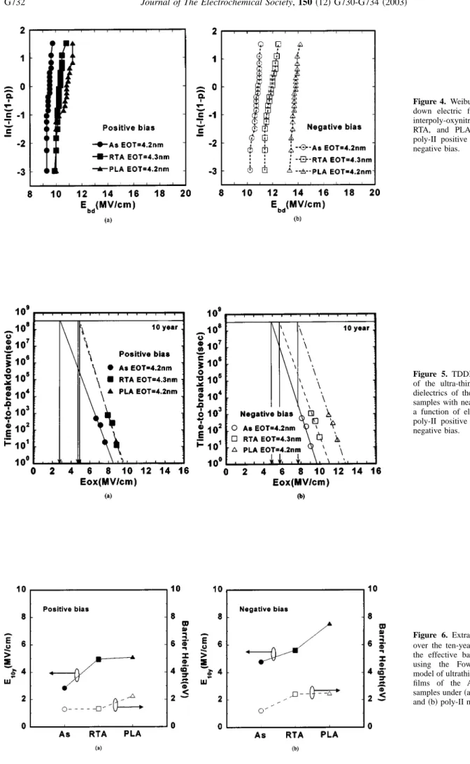
Figure 4 presents the Weibull plots of the breakdown electric field of the ultrathin interpoly-oxynitride dielectrics with nearly the same EOT in both polarities, respectively. The samples with anneal-ing presented a higher breakdown electric field than the control sample under both positive共Fig. 4a兲 and negative bias 共Fig. 4b兲. In particularly, for the poly-II injection of the N2O plasma-annealed sample, significant improvement of the breakdown electric field was observed共negative bias兲. This fact is attributable to the introduction of oxygen into both the poly-II/nitride interface and the bulk of the nitride film. Figure 5a is a plot of the time-dependent-dielectric-breakdown 共TDDB兲 lifetime projection of the ultrathin interpoly-oxynitride dielectrics with nearly the same EOT under poly-I injec-tion共positive bias兲 as a function of electric field. After annealing, a large increase in the electric field over the projected 10-year lifetime was contemplated, due to the improvement of the dielectric near the nitride/poly-I interface. Under negative bias, as shown in Fig. 5b, the N2O plasma-annealed sample exhibited a fairly high electric field up to 7.25 MV/cm over the projected ten-year lifetime because of the superior quality of the interpoly-oxynitride dielectrics. The reduction of the leakage current may lead to fewer defects in the oxynitride film following the N2O plasma annealing.
Figure 6 plots both polarities of the extrapolated electric field over the ten-year lifetime (E10y) and the effective barrier height (B) determined by using the Fowler-Nordheim 共F-N兲 model of ultrathin interpoly-oxynitride dielectrics under various annealing processes with nearly the same EOT. The effective barrier height was obtained by plotting the J-E characteristics in the form of an F-N plot (J/E2 vs. 1/E兲.17 Straight lines were obtained for all
Figure 2. TEM images of the interpoly-oxynitride films for the共a兲 control
sample; 共b兲 RTN2O annealed sample; and 共c兲 high density N2O plasma-annealed sample.
Figure 3. Current density vs. electric field 共J-E兲 characteristics of ultrathin interpoly-oxynitride films of the con-trol sample共As兲 and the samples un-der RTN2O 共RTA兲 and high density N2O plasma annealing 共PLA兲 under 共a兲 poly-II positive bias and 共b兲 poly-II negative bias.
Figure 4. Weibull plots of the break-down electric field of the ultrathin interpoly-oxynitride films of the As, RTA, and PLA samples under 共a兲 poly-II positive bias and 共b兲 poly-II negative bias.
Figure 5. TDDB lifetime projection of the ultra-thin interpoly-oxynitride dielectrics of the As, RTA, and PLA samples with nearly the same EOT as a function of electric field under 共a兲 poly-II positive bias and 共b兲 poly-II negative bias.
Figure 6. Extrapolated electric field over the ten-year lifetime (E10y) and the effective barrier height obtained using the Fowler-Nordheim 共F-N兲 model of ultrathin interpoly-oxynitride films of the As, RTA, and PLA samples under共a兲 poly-II positive bias and共b兲 poly-II negative bias.
samples, indicating that F-N tunneling was the major conducting mechanism. Transport due to F-N tunneling is specified by J ⫽ C1E2exp(⫺B/E), where E is the field, and C
1 and B are constants for the effective mass and barrier height. Indeed, the ef-fective barrier height and the extrapolated electric field over the ten-year lifetime increased after annealing, especially after high den-sity N2O plasma annealing. Not only poly-I but also poly-II injec-tions exhibit the highest B and E10y values for N2O plasma-annealing interpoly-oxynitride. This result is proven by Fig. 4, which shows the introduction of oxygen into both the polysilicon/ nitride interface and the bulk of the nitride film. This would increase the effective barrier height of the interpoly-oxynitride dielectric ap-proaching that of silicon dioxide thin films. Figure 7 shows the electron trapping characteristics of both polarities for all samples under a constant current stress of 1 mA/cm2. The figure shows that the additional annealing of interpoly-oxynitride produced a smaller
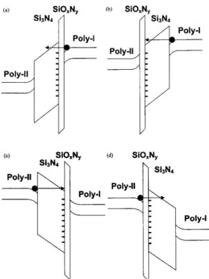
voltage shift than that of control sample. For poly-I injection, shown in Fig. 7a, N2O plasma annealing generated the smallest voltage shift, implying that the lowest charge was trapped near the nitride/ poly-I interface. Nevertheless, an early failure and larger trapping rate was observed for the RTA sample. This phenomenon can be explained by the band diagrams in Fig. 8a for the RTA sample and 共b兲 for the PLA sample under poly-I injection. The Si3N4/SiOxNy structure was proposed above, and the large stress-induced-defects at the Si3N4/SiOxNy interface contributed to the early failure and larger trapping rate for the RTA sample. However, for the poly-II injection shown in Fig. 7b, the N2O plasma-annealed sample had a larger trapping rate, which result is consistent with the fact that the some stress-induced-charge trapped at the SiOxNy/Si3N4 interface under such annealing is detectable from the band diagram in Fig. 8d. Therefore, under N2O plasma annealing, defects and traps were eliminated near the poly-I/oxynitride interface, while a few stress-induced-defects might have existed at the SiOxNy/Si3N4interface.
In conclusion, Table I summarizes data concerning an ultrathin (EOT⬃ 42 Å) and highly reliable interpoly-oxynitride film formed by additional annealing. For a similar oxide thickness, high density N2O plasma-annealed sample presents is more reliable than the RTN2O annealed sample.
Conclusion
This work examined the ultrathin (EOT⫽ 42 Å) interpoly-oxynitride films with high density N2O plasma and RTN2O anneal-ing. N2O plasma annealing led to the incorporation of a high con-centration of oxygen into the poly-II/nitride interface and a reduction of the trap density. Accordingly the interpoly-oxynitride dielectrics were made more reliable with a lower gate leakage cur-rent, a higher breakdown electric field, a longer ten-year lifetime, and larger effective barrier height. The oxynitride is very suitable for use in the next generation EEPROM.
Figure 7. Electron trapping character-istics of the ultrathin interpoly-oxynitride of the As, RTA, and PLA samples under共a兲 poly-II positive bias (J⫽ 1 mA/cm2) and共b兲 poly-II nega-tive bias (J⫽ ⫺1 mA/cm2).
Table I. Summary of the breakdown electric field„Ebd…, effective
barrier height„⌽B… and the extrapolated electric field over the
ten-year lifetime„E10y… of the ultrathin interpoly-oxynitride film
of the As, RTA, and PLA samples, respectively. EOT
共Å兲 共MV/cm兲Ebd 共eV兲⌽B 共MV/cm兲E10y
As-deposited 42 9.4共⫹兲 1.29共⫹兲 2.84共⫹兲
Acknowledgments
The authors thank the National Science Council of the Republic of China, Taiwan, for financially supporting this research under con-tract no. NSC92-2215-E009-022. The National Nano Device Labo-ratory, R.O.C., is also appreciated for their technical assistance.
National Chiao-Tung University assisted in meeting the publication costs of this article.
References
1. C. S. Lai, T. F. Lei, and C. L. Lee, IEEE Trans. Electron Devices, 43, 326共1996兲. 2. L. Faraone, IEEE Trans. Electron Devices, 33, 1785共1986兲.
3. S. L. Wu, T. Y. Lin, C. L. Lee, and T. F. Lei, IEEE Electron Device Lett., 14, 113
共1993兲.
4. S. L. Wu, C. Y. Chen, T. Y. Lin, C. L. Lee, T. F. Lei, and M. S. Liang, IEEE Trans. Electron Devices, 44, 153共1997兲.
5. C. L. Cha, E. F. Chor, H. Gong, A. Q. Zhang, and L. Chan, Tech. Dig. - Int. Electron Devices Meet., 1997, 82.
6. N. Matsuo and A. Sasaki, IEEE Trans. Electron Devices, 42, 1340共1995兲.
7. S. Holland, IEEE Trans. Nucl. Sci., 42, 423共1995兲.
8. J. W. Lee, C. L. Lee, T. F. Lei, and C. S. Lai, IEEE Trans. Electron Devices, 48, 743共2001兲.
9. C. H. Kao, C. S. Lai, and C. L. Lee, IEEE Electron Device Lett., 44, 526共1997兲. 10. C. H. Kao, C. S. Lai, and C. L. Lee, IEEE Trans. Electron Devices, 45, 1927
共1998兲.
11. W. L. Yang, T. S. Chao, C. M. Cheng, T. M. Pan, and T. F. Lei, IEEE Trans. Electron Devices, 48, 1304共2001兲.
12. L. Faraone, R. D. Vibronek, and J. T. Mcginn, IEEE Trans. Electron Devices, 32, 577共1985兲.
13. H. Sato, H. Kato, Y. Ohki, S. S. Kwang, and T. Noma, in International Symposium on Electrical Insulating Materials, ISEIM 2001, IEEJ Technical Committee on Dielectrics and Electrical Insulation, and IEEE Dielectrics and Electrical Insulation Society, p. 148共2001兲.
14. T. Arakawa and H. Fukada, Electron. Lett., 30, 361共1994兲.
15. T. M. Pan, T. F. Lei, W. L. Yang, C. M. Cheng, and T. S. Chao, IEEE Electron Device Lett., 22, 68共2001兲.
16. W. H. Lin, K. L. Pey, Z. Dong, S. Y.-M. Choi, M. S. Zhou, T. C. Ang, C. H. Ang, W. S. Lau, and J. H. Ye, IEEE Electron Device Lett., 23, 124共2002兲.