Controlling hole-transport in aluminum tris (8-hydroxyquinoline), Alq 3 -based organic
light emitting diodes to improve the device lifetime by an oxidized transport layer
Mathew K. Mathai, Fotios Papadimitrakopoulos, and Bing R. Hsieh
Citation: Journal of Applied Physics 95, 8240 (2004); doi: 10.1063/1.1728289
View online: http://dx.doi.org/10.1063/1.1728289
View Table of Contents: http://scitation.aip.org/content/aip/journal/jap/95/12?ver=pdfcov Published by the AIP Publishing
Articles you may be interested in
p -type Zn 1 x Mg x O films with Sb doping by radio-frequency magnetron sputtering Appl. Phys. Lett. 89, 202102 (2006); 10.1063/1.2388254
p -type conduction in wide-gap Zn 1 x Mg x O films grown by ultrasonic spray pyrolysis Appl. Phys. Lett. 87, 092101 (2005); 10.1063/1.2035326
Enhancement of p -type conductivity in nanocrystalline Ba Ti O 3 ceramics Appl. Phys. Lett. 86, 082110 (2005); 10.1063/1.1864232
Properties of nitrogen-implanted p-type ZnO films grown on Si 3 N 4 / Si by radio-frequency magnetron sputtering
Appl. Phys. Lett. 84, 5040 (2004); 10.1063/1.1763640
p-type semiconducting Cu 2 O–CoO thin films prepared by magnetron sputtering J. Vac. Sci. Technol. A 21, 1336 (2003); 10.1116/1.1580491
A salt containing polymer, called an oxidized transport layer 共OTL兲, was investigated for hole injection and transport into Alq3-based multilayered organic light emitting diode共OLED兲 devices.
The OTL comprises an aryldiamine containing hole transport polymer binder with a corresponding low molecular weight radical cation salt. We demonstrate herein that the OTL behaves like a tunable resistor for holes, and its hole-transport properties can be controlled by the salt concentration and thickness of the OTL. Based on a careful analysis of the current density–voltage (J – V) device characteristics as a function of the above parameters, electron/hole currents were balanced to minimize oxidative degradation of Alq3. It was found that an OLED device (ITO/OTL/NPB/Alq3/CsF/Al) with a 5000 Å thick OTL at 5% salt concentration operated with a
half-life exceeding 1000 h at a constant current of 10 mA/cm2. Similar devices with 2.5% and 10% salt doping showed an order of magnitude lower half-life attributed to unbalanced carrier concentrations. Moreover, by demonstrating that the majority of the field drops across the Alq3
layer, the doping level as opposed to OTL thickness was established as the primary contributor controlling hole transport in these OLEDs. This beneficial behavior is, however, observed only above a certain OTL thickness in the vicinity of 5000 Å. © 2004 American Institute of Physics.
关DOI: 10.1063/1.1728289兴
I. INTRODUCTION
Controlling molecular design and device architecture has paved the way to realize organic based optoelectronics. Among different potential applications which have emerged in the past decade, the field of organic light emitting diodes
共OLEDs兲 based on aluminum tris 共8-hydroxyquinoline兲
(Alq3) as an active luminescent material has shown
tremen-dous growth since its inception.1,2 However, there are still various obstacles that need to be overcome before reaching extensive commercialization and one of the major challenges is the improvement of device operating lifetime.
Contributing factors to the decay of device performance over time include reaction of Alq3 with the cathode and its delamination,3 indium diffusion into the organic layers,4 interdiffusion,5 chemical degradation,6and crystallization of the same.7Careful engineering of device fabrication by ma-nipulating different parameters such as the purity and choice of materials,8,9 the rate of film growth during organic layer deposition,10 the vacuum under which devices are fabricated,11and encapsulation12 have improved device per-formance. At the same time, however, the results of Aziz et al.13 and our own,14 clearly underline the importance of curbing the intrinsic degradation associated with the forma-tion of caforma-tionic Alq3species in OLEDs that utilize this
mol-ecule as either a light-emitter, host material for emissive dyes, or electron transporting layer共ETL兲. More recently, the results of Kondakov et al. have demonstrated the effect of trapped immobile positive charge within the OLED which act as nonradiative recombination centers.15 Accordingly, it can be concluded that in order to reduce the intrinsic degra-dation in Alq3OLEDs a better understanding and control of
the bipolar nature of charge transport through these devices is required.
In this regard, the development of hole transport layers
共HTL兲 for OLEDs has proceeded in two related but
appar-ently contradictory directions. On one hand, attempts have been made to reduce the injection barriers at device inter-faces in order to facilitate hole injection into the Alq3
devices.16This has been indicated to result in improved de-vice efficiency16 and apparent stability after 10 h.17 On the other hand, the results of Aziz et al.13signify the importance impeding the transport of holes into the Alq3layer in order to
improve device lifetimes. To this extent, venues such as blending HTL and ETL layers,18 using dyes as trap sites within the HTL,19 hole blocking layers,20 and inducing the formation of emissive sites by dye doping within the HTL itself21 have been explored to achieve the same. These re-search initiatives—one to improve hole injection from the anode and the other to impede the hole transport into the Alq3 layer—address different aspects of bipolar transport in
these devices. Reduction of hole interfacial barriers ensures
a兲Author to whom correspondence should be addressed; electronic address: [email protected]
8240
0021-8979/2004/95(12)/8240/7/$22.00 © 2004 American Institute of Physics
ease of hole injection and reduces heating effects which are known to contribute to device degradation. However, among such optimized devices, one has to be concerned with reduc-ing the uncontrolled injection of holes, especially at higher device operating voltages.
Based on the above discussion it is apparent that an ap-proach combining both reduced barriers to hole injection, and modulated hole transport are needed to further improve device lifetime. The balance of charge carrier injection should persist over all applied fields, which is important for display applications, where gray scale is controlled by vary-ing the applied drive voltage. This imposes additional re-quirements on the choice of materials and device architecture in order to extend the regime of balanced charge transport to larger operating voltages.
In this paper we demonstrate the above device perfor-mance enhancing strategy by introducing a salt containing polymer layer between the ITO anode and a conventional hole transporting layer similar to the work of Yamamori et al.22 This layer is henceforth referred to as the oxidized transporting layer 共OTL兲 and consists of a polycarbonate of N,N
⬘
-bis共3-hydroxymethyl兲-N,N⬘
-bis共phenyl兲 benzidine and diethylene glycol共PC-TPB-DEG兲 loaded with the SbF6⫺salt of N,N,N
⬘
,N⬘
-tetrakis共4-methylphenyl兲 benzidine (TMTPD"⫹ SbF6⫺).23 These components of the OTL along with the other molecules used in this study are shown in Fig. 1. The conductivity of the OTL can be varied over two or-ders of magnitude by adjusting the concentration of the oxi-dizing organic moieties in the film.24,25The tunable conduc-tivity ensures that the number of holes being injected into the Alq3 layer in OTL modified devices are optimized. In addi-tion, the presence of the salt in the OTL ensures minimized interfacial barriers to the injection of holes by means of al-tering the ionization potential of ITO and thinning of the tunneling barrier at the ITO/OTL interface.26 Based on this, we currently show that the OLEDs thus fabricated exhibit optimized quantum efficiencies and lifetimes. As the conduc-tivity of the OTL is changed to be less or more than an optimum value, device performance degrades. Thus, as indi-cated in the schematic of Fig. 2, OTL acts both to facilitate hole injection through ITO共which reduces interfacial heatingeffects兲, along with providing a variable resistor to minimize excess hole injection into Alq3 共that optimizes device
life-time兲.
II. EXPERIMENT
All the devices made in this study were fabricated on indium tin oxide 共ITO兲 coated glass substrates 共Thin Film Devices兲. The ITO-coated substrates were cleaned by scrub-bing gently with detergent solution, washing in distilled wa-ter and organic solvents, followed by oxygen plasma treat-ment for 10 min. The OTL was fabricated by spin casting a 25 mg/ml solution of polymer and salt in methylene chloride onto the ITO-coated glass substrate at 1000 rpm. Under these conditions, the thickness of the OTL obtained is 5000 Å. A series of PC-TPD-DEG solutions were prepared and into these solutions, different salt concentrations were added by weight percent with respect to the polymer weight in the solutions. The films obtained from these solutions were seen to have a thickness variation of less than 150 Å as measured by profilometry. In experiments where the thickness of the OTL is deliberately varied, the desired thickness was achieved by using a diluted solution of the OTL and by in-creasing the speeds at which spin casting was carried out.
Two sets of experiments were performed to study the effect of the OTL on OLEDs based on Alq3. In the first set of experiments, three types of devices were fabricated as follows: single layer OTL devices 共ITO/OTL/Al兲, OTL modified Alq3 devices (ITO/OTL/NPB/Alq3/CsF/Al),
bi-layer devices (ITO/NPB/Alq3/CsF/Al), where ITO and
CsF/Al are the anode and cathode, respectively. The CsF layer was deposited in order to improve injection of electrons from the Al cathode.27The deposition of the organic materi-als, CsF, and metal electrode was carried out in an Edwards Auto 306 high vacuum coater at 1.5⫻10⫺6 Torr. The
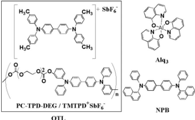
thick-FIG. 1. Chemical structures of the compounds used in this study. The oxi-dized transport layer 共OTL兲 consists of a hole transporting polycarbonate PC-TPB-DEG containing varying amounts of the SbF6⫺salt of TMTPD⫹. The structures of N,N⬘-bis(naphthalen-1-yl)-N,N⬘-bis(phenyl)benzidine
共NPB兲 and Alq3are also shown.
FIG. 2. Schematic illustrating the charge transport of holes and electrons in
共a兲 conventional Alq3devices with NPB as hole transport layer without any OTL and共b兲 OTL modified Alq3OLEDs共Ref. 26兲. In 共b兲 both electron and hole injection barriers are reduced. The variable resistance of the OTL de-termines the number of holes being injected into the Alq3 light-emitting layer to reduce formation of Alq3⫹cationic species.
8241 J. Appl. Phys., Vol. 95, No. 12, 15 June 2004 Mathai, Papadimitrakopoulos, and Hsieh
After fabrication, all the devices were transferred to a nitrogen glove box without exposure to oxygen or moisture for characterization and testing. Current density–voltage (J – V) characteristics were obtained on a Hewlett Packard 4155 semiconductor parameter analyzer and light output was measured by a calibrated Newport UV-818 photodetector. While measuring OLED external quantum efficiency, the ab-sorption of light emitted in the Alq3layer by the OTL, before
it exits the device has to be taken into consideration as in-creasing salt loading increases its absorption in the visible range. In order to achieve this, transmittance values were obtained for OTL films with the same thickness and salt loading as utilized in the devices. The actual light output of the device was obtained by using the transmittance as a cor-rection factor for the light measured by the photodiode as each device was tested.
III. RESULTS AND DISCUSSION A. Single layer OTL devices
The PC-TPB-DEG polymer consists of HTL type mono-mer units separated by saturated ether linkages. The addition of the TMTPD"⫹ SbF6⫺ salt to this polymer results in the formation of a charge transfer state with an absorption cen-tered at around 1466 nm共spectrum not shown兲. Thus excess intrinsic charge carriers proportional to the salt loading are generated in the OTL. The result of this is a higher conduc-tivity of the OTL with increasing salt concentration in the polymer.
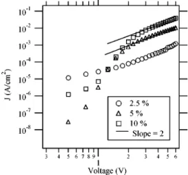
The relationship between the conductivity of the OTL and the extent of salt loading has been studied by fabricating single layer devices of the OTL containing different salt con-centrations sandwiched between ITO and Al contacts 共ITO/ OTL/Al兲. Based on the large band offset between Al and OTL interface with respect to electron injection, along with the fact that these materials are primarily hole transporters,22 we can safely assume that the current being measured is hole dominated. For 5% and 10% salt loading, the current density–voltage (J – V) characteristics of these devices show the typical behavior of unipolar charge transport in an amor-phous material with an initial Ohmic region followed by cur-rent turn on at around 1 V共Fig. 3兲. This turn on is followed by an initial higher slope J – V characteristic, which quickly saturates to a J – V2 type behavior above an applied voltage of 2 V. For 2 V and above, the measured current at any applied field increases with increasing salt concentration. This result is in agreement with conductivity measurements carried out on the OTL共Ref. 28兲 indicating that the current
values can be tuned over two orders of magnitude while still maintaining the J – V2 behavior. The reproducible, higher magnitude current observed for the 2.5% doped device be-low 2 V could be due to lesser trapping of holes in the presence of lower salt concentration or preferential confine-ment of salt to the ITO/OTL interface. However, since in the typical OLEDs the operating voltages extend beyond this Ohmic regime, to the first approximation it can be seen that salt loading in the OTL should control the hole-current pass-ing through the device. This property of the OTL will now be considered within the device architecture of conventional Alq3 OLEDs.
B. The effect of the OTL on Alq3-based OLEDs
The comparison of the J – V characteristics of conven-tional bilayer Alq3 devices and OTL modified Alq3 devices
in which the salt concentration in the OTL is varied is shown in Fig. 4. The schematic indicates the sequence of deposited layers on the ITO anode. All OTL modified devices show an initial Ohmic J – VI regime below 2 V followed by a power law behavior of J – Vmwith m varying between 7 and 10. At higher applied fields, the steep increase in current density is reduced with the value of m plateauing at m⫽2 above 6 V. This behavior is in contrast to the typical ITO/NPB/Alq3/CsF/Al device made without the OTL as
shown in Fig. 4, where the steeper power law behavior of J – Vm (m⭓5) persists for voltages above 6 V.29 The light emission onset共data not shown兲 is at the same applied volt-age at which the device turn on occurs, indicating that above ca. 2.5 V both holes and electrons are present at the recom-bination interface.
In addition to the appearance of the J – V2 behavior at
low voltage共⬃6 V兲, increasing the salt concentration in the OTL results in higher current levels for any given applied field after the turn on voltage. These observations can be explained on the basis of additional hole current in these devices due to the increased conductivity of the OTL as al-ready shown in Fig. 3. However, consideration has to be given to the field distribution over the cross section of the device and barriers to charge injection at the device anode as
FIG. 3. J – V data plotted for single layer OTL devices with varying (TMTPD⫹SbF6⫺) salt concentration in the OTL.
the salt concentration in the OTL is varied. In order to un-derstand the contribution of these factors, we have varied the thickness and hence the applied field for the active layers
共NPB, Alq3, and OTL兲 and studied the trends observed in
J – V characteristics. In all these devices, the salt concentra-tion in the OTL was maintained at 5% by weight with respect to the polymer.
C. Variation of thickness of OLED layers
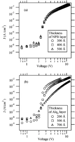
The results of the thickness variation of NPB and Alq3
are shown in Figs. 5共a兲 and 5共b兲, respectively. These results agree with those reported for bilayer devices without any ITO modifying layers.29 Increasing the thickness of NPB gives rise to a less pronounced decrease in current densities for any applied voltage as opposed to the case of Alq3
thick-ness variation. Furthermore, the varying thickthick-ness of the NPB layer does not affect the current level at which the transition to the J – V2is observed. On the other hand, varia-tion in Alq3 thickness affects not only the voltage at which
the J – V7 – 10to J – V2 transition occurs but also the value of m in the power law regime (J – V7 – 10). The thinner the Alq3
layer, the steeper the J – V characteristics appeared in this regime. Direct30and indirect31measurements of electric field distribution for bilayer Alq3 OLEDs indicate that the major-ity of the applied electric field drops across the Alq3 layer. The results shown in Fig. 5 indicate that in spite of the pres-ence of the thick OTL, still a considerable fraction of the applied field drops across the Alq3 layer for these OLEDs.
With this realization, the OTL thickness was varied in order to deliberately alter the electric field applied across it. Any similarity between the trends observed in this experi-ment and those observed in Fig. 4 for varying salt concen-tration will indicate field variation and not conductivity as being the possible reason for the current modulation. As shown in Fig. 6, as the OTL thickness decreases, the J – V
characteristics in the trap charge limited regime 共TCL, J – V7 – 10) approach that of the bilayer device共no OTL兲. This behavior also persists above the TCL regime where the J – Vmcharacteristics approach the slope of m⫽5, shown for the bilayer device. As the OTL thickness increases, the slope decreases to a value of 2 shown for the 5000 Å thick OTL devices of Fig. 4. This indicates that the contribution of the OTL to the formation of the J – V2 regime in the device is reduced and there is discernable field variation across the OTL as the thickness is varied from 5000 to 900 Å. How-ever, the trend observed in this case is in contrast to the device characteristics shown in Fig. 4, where the J – V2 be-havior persists in spite of varying salt concentration.
In addition, on comparing the device modified with a 900 or 2000 Å thick film of OTL and the conventional bi-layer device, it is observed that above the turn on voltage the former has an even higher magnitude of current within the range of applied field investigated in spite of the presence of the additional layer of OTL. This indicates that in OTL modified devices the barrier to hole injection at ITO is re-duced as compared to the bilayer device. As was explained earlier in the schematic representation shown in Fig. 2, this is one of the requirements for improved OLED performance. The investigations of the injection of electrons into Alq3with
LiF and CsF modified cathodes27,32 have proved that such modified cathodes have minimized electron injection barriers
FIG. 4. J – V data plotted for multilayer OLED devices with varying (TMTPD⫹SbF6⫺) salt concentration in the OTL. For comparison, the J – V characteristics for a typical bilayer device are also shown, along with lines drawn to guide the eye with respect to m⫽2 and 5 for J – Vm.
FIG. 5. J – V data plotted for devices 共ITO/OTL
(5000 Å)/NPB/Alq3/CsF/Al) with varying thickness of共a兲 NPB and 共b兲 Alq3, while keeping the respective (Alq3and NPB兲 layer thickness constant at 500 Å. The OTL in all cases was loaded with 5% salt.
8243 J. Appl. Phys., Vol. 95, No. 12, 15 June 2004 Mathai, Papadimitrakopoulos, and Hsieh
with respect to the Alq3 layer. Hence we can conclude that
for the Alq3 OLEDs whose anode and cathode have been
modified with OTL and CsF, respectively, the interfacial bar-riers at the electrodes for hole and electron injection into the Alq3 layer are minimized. Given this result, the modulation
of the salt concentration in the OTL and hence its conduc-tivity should be the governing factor in the variation of the J – V characteristics of the OTL modified Alq3 devices.
33
Since the OTL primarily transports holes, it can be con-cluded that in Fig. 4, the variation in the J – V characteristics is due to variation in the number of holes being injected into the Alq3 layer. Based on a certain capture cross section of
holes for Alq3 共Ref. 29兲 at the NPB/Alq3carrier
recombina-tion interface34 such modulation of holes should control the extent of formation of excitons and cationic species of Alq3 which is demonstrated by measuring the quantum efficien-cies and lifetimes of these devices.
D. The effect of OTL on quantum efficiencies and lifetimes of OLEDs
The variation of external quantum efficiency共QE兲 plot-ted versus device current density is shown in Fig. 7 for dif-ferent salt concentrations. The QE is seen to start from a comparatively lower value for the OLED with the lowest concentration of salt loading in the OTL 共2.5%兲, rise to a maximum for the OLED with intermediate salt loading共5%兲, and fall again for the one with 10% loading of salt in the OTL. Based on the above discussion on the role played by the OTL, the initial increase in QE as the salt loading is increased can be explained on the basis of a higher concen-tration of hole injection into the Alq3 layer as the
conductiv-ity of the OTL is raised, thus resulting in the formation of more excitons within Alq3. Further increase in the salt
load-ing, while improving hole injection into the Alq3 layer,
quickly surpasses the available electrons. Since the only bar-rier to keep excess holes within the recombination interface is the low hole mobility of Alq3,35 above a certain point these holes contribute to leakage current in the device, thus decreasing QE. Moreover, it has been argued by Young et al. that cationic species could also be responsible for fluores-cence quenching in dye doped Alq3 devices which are hole
current dominated.36
An added benefit of the OTL is reflected in the low variation of the slope in the QE versus J characteristics, at-tributed to the hole and electron balance within the Alq3
layer over a wider range of current density. On the other hand, the bilayer device 共without OTL兲 exhibits a much greater variation in quantum efficiency over the range of cur-rent density values displayed in Fig. 7. This large variation even results in a slightly higher QE compared to the opti-mized 5% salt-loaded OTL modified device at higher current densities. In this regime, unlike the OTL device, which con-trols the hole current, the bilayer device provides an exces-sive amount of holes. This, together with the field enhanced mobility of electrons, will result in greater radiative recom-bination and hence, higher QE. However, at these elevated fields a complete capture of holes is not guaranteed as further supported by the lifetime measurements described below. Thus, from the perspective of QE, the OTL devices display enhanced performance as opposed to the bilayer device only for moderate fields共ca. 6 V兲. At higher fields, QE is partially sacrificed in order to ensure efficient hole capture within the Alq3 layer thus ensuring increased lifetime.
Based on the above argument, one might wonder why the 10% loaded OTL device has such a lower QE. In order to address this point, one has to account that by insertion of the OTL, all barriers to hole injection are substantially reduced
关as contrasted in Figs. 2共a兲 and 2共b兲 as well as demonstrated
in Fig. 6兴. However, the bilayer device, lacking OTL, still has the ITO/NPB interfacial barrier to overcome. Thus, when voltage is increased in the bilayer device, this barrier pro-vides some form of impediment to hole injection unlike that
FIG. 6. J – V characteristics plotted for varying thickness of the OTL. Salt concentration in the OTL was kept constant at 5% by weight. For compari-son, the J – V characteristics for a typical bilayer device are also shown, along with lines drawn to guide the eye with respect to m⫽2 and 5 for
J – Vm.
FIG. 7. Variation of OLED external quantum efficiencies共corrected for the OTL absorption兲 as a function of current density, for different salt concen-trations in 5000 Å thick OTL. For comparison purpose, the external quan-tum efficiency for a typical bilayer device is also shown.
of the 10% OTL device, which has no hole interfacial im-pediments.
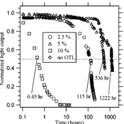
The devices fabricated with varying salt concentration in the OTL were tested for operational lifetimes at a fixed cur-rent density of 10 mA/cm2. Figure 8 illustrates the normal-ized fall in light output for these devices. As mentioned be-fore, the relative field variation across the OTL is minimal for varying salt concentration in these devices; however, the voltages applied to the devices vary due to the additional field required to pass the same current through the devices. It is important to note that in reporting the lifetimes of these devices, there are different degradation processes taking place. The abrupt and catastrophic failure of devices is due to cathode delamination and degradation and is superimposed over the more gradual oxidative degradation occurring in these devices. Migration of ions under forward bias within the OTL has been ruled out as there is no observable salt migration for single layer OTL devices when 10 mA/cm2 was applied over extended periods. The 2.5% OTL device shows a half-life of 180 h and abrupt failure over the next 20–30 h. The 5% OTL device shows a higher lifetime by as much as an order of magnitude with a half-life exceeding 1000 h. The 10% OTL device on the other hand shows dras-tically reduced lifetime decay with a half-life of less than 1 h. The decay in this case occurs even before the degradation associated with cathode delamination.
The lifetime measurements clearly indicate the detrimen-tal effect the presence of the cationic species has on the device performance when comparing the performance of the 5% and 10% doped OTL devices. The higher rate of hole injection into the Alq3 layer for the 10% doped OTL device results in a rapid decay of the light output from the device. Based on the analysis of the quantum efficiency measure-ments, it seems that the 2.5% device should also show life-times similar to that of the 5% device. However, the voltage drop required to pass 10 mA/cm2 in the 2.5% device is higher than the 5% or 10% doped OTL devices thus leading to considerable heating effects. The high efficiency of the 5% device and its longer lifetime imply a better balance in the multiplicity of parameters including minimal formation of
cationic Alq3⫹ light quenching species 13,36
and trap sites due to oxidative degradation of Alq3.
14
Thus the OTL enables the optimization of device performance by tuning the relative transport of holes with respect to electrons in these devices.
E. Controlled hole injection by means of OTL
In any bipolar device the current measured is the sum of electron and hole currents. In both conventional bilayer de-vice schemes and OTL modified dede-vices based on Alq3, the
field is seen to drop mostly across the Alq3 layer thus
indi-cating that the bipolar charge transport through this layer plays a major role in determining the evolution of the J – V characteristics with respect to the relative contribution of electrons and holes to the measured current. Compounding this fact is the variation of the hole and electron mobilities of Alq3 with applied field and interfacial charge accumulation
at the Alq3/NPB interface. The electron mobility (1.4 ⫻10⫺6 cm2V⫺1s⫺1) of Alq
3 is much higher than the hole
mobility (2.0⫻10⫺8cm2V⫺1s⫺1) at low applied fields.35 This relatively high electron mobility along with the CsF-assisted reduced electron injection barrier into this layer en-sures that the charge present in Alq3 is dominated by the
formation of an electron cloud, confined by the high lowest unoccupied molecular orbital of NPB. However, as the ap-plied field increases, the field assisted mobility of Alq3
causes the difference in electron and hole mobilities to reduce.37 This, along with accumulated holes at the NPB/Alq3 interface, results in enhanced hole current in the
device.38 Given the occurrence of oxidative degradation, fluorescence quenching, and a high value of m in the J – Vm
characteristics of conventional bipolar devices, such an en-hanced hole current can prove detrimental to device perfor-mance. On the other hand, the introduction of a resistor in the form of the OTL at the hole injecting anode ensures the modulation of such charge buildup, thus preventing exces-sive hole injection due to field-enhanced hole mobility of Alq3which is bound to occur at higher applied voltages. The
modulation of hole current by the OTL thus allows for im-proved device quantum efficiency and lifetimes by directly addressing the issue of hole modulation in Alq3 based
OLEDs at the expense of a slightly higher device operating voltage.
IV. CONCLUSION
The results presented above have demonstrated the im-portance of controlling the bipolar characteristics of devices utilizing Alq3 as the emitting layer. Excess hole injection in Alq3-based OLEDs leads to oxidative degradation within the Alq3 layer and the formation of cationic species that quench
electroluminescence of the devices. Both the improvement in hole injection and the modulation of hole concentration in the Alq3 layer can be achieved by means of an OTL. The
latter is achieved by finetuning the conductivity of the OTL by varying the concentration of salt in the same. These OTL modified Alq3 OLEDs are devices whose properties are
gov-erned more by the conductivity of the active layers, rather than interfacial barriers. This leads to the occurrence of a J – V2 type behavior in individual layers, resulting in
bal-FIG. 8. Lifetimes of OTL modified OLEDs with varying salt concentration in the OTL. For comparison purpose, the lifetime for a typical bilayer device is also shown.
8245 J. Appl. Phys., Vol. 95, No. 12, 15 June 2004 Mathai, Papadimitrakopoulos, and Hsieh
thors also gratefully acknowledge Kodak Corporation for kindly providing NPB as well as Dr. Nguyen Thuc-Quyen for helpful discussions.
1C. W. Tang and S. A. VanSlyke, Appl. Phys. Lett. 51, 913共1987兲. 2
A. Tullo, Chemical and Engineering News共American Chemical Society, Washington, D.C., 2001兲, Vol. 79, pp. 49–54.
3J. McElvian, H. Antoniadis, M. R. Hueschen, J. N. Miller, D. M. Roitman, J. R. Sheats, and R. L. Moon, J. Appl. Phys. 80, 6002共1996兲.
4S. T. Lee, Z. Q. Gao, and L. S. Hung, Appl. Phys. Lett. 75, 1404共1999兲. 5
M. Fujihira, L.-M. Do, A. Koike, and E.-M. Han, Appl. Phys. Lett. 68, 1787共1996兲.
6L. S. Liao, J. He, X. Zhou, M. Lu, Z. H. Xiong, Z. B. Deng, X. Y. Hou, and S. T. Lee, J. Appl. Phys. 88, 2386共2000兲.
7
H. Aziz, Z. Popovic, S. Xie, A.-M. Hor, N.-X. Hu, C. Tripp, and G. Xu, Appl. Phys. Lett. 72, 756共1998兲.
8Y. Shirota, K. Okumoto, and H. Inada, Synth. Met. 111–112, 387共2000兲. 9S. A. Van Slyke, C. H. Chen, and C. W. Tang, Appl. Phys. Lett. 69, 2160
共1996兲.
10
L. F. Cheng, L. S. Liao, W. Y. Lai, X. H. Sun, N. B. Wong, C. S. Lee, and S. T. Lee, Chem. Phys. Lett. 319, 418共2000兲.
11A. Bohler, S. Dirr, H. H. Johannes, D. Ammermann, and W. Kowalsky, Synth. Met. 91, 95共1997兲.
12P. E. Burrows, V. Bulovic, S. R. Forrest, L. S. Sapochak, D. M. McCarty, and M. E. Thompson, Appl. Phys. Lett. 65, 2922共1994兲.
13H. Aziz, Z. D. Popovic, N.-X. Hu, A.-M. Hor, and G. Xu, Science 283, 1900共1999兲.
14F. Papadimitrakopoulos, X. M. Zhang, D. L. Thomsen III, and K. A. Higginson, Chem. Mater. 8, 1363共1996兲.
23B. R. Hsieh, Xerox Corporation, 1998, US Patent 5,853,906. 24
B. R. Hsieh, Polym. Prepr.共Am. Chem. Soc. Div. Polym. Chem.兲 43, 452
共2002兲.
25
Y. Shen, K. Diest, M. H. Wong, B. R. Hsieh, D. H. Dunlap, and G. G. Malliaras, Phys. Rev. B 68, 081204共1兲 共2003兲.
26C. Ganzorig and M. Fujihira, Appl. Phys. Lett. 77, 4211共2000兲. 27P. Piromreun, H. Oh, Y. Shen, G. G. Malliaras, J. Campbell, and P. J.
Brock, Appl. Phys. Lett. 77, 2403共2000兲. 28
B. R. Hsieh, Polym. Prepr.共Am. Chem. Soc. Div. Polym. Chem.兲 43, 452
共2002兲.
29P. E. Burrows, Z. Shen, V. Bulovic, D. M. McCarty, S. R. Forrest, J. A. Cronin, and M. E. Thompson, J. Appl. Phys. 79, 7991共1996兲.
30M. Hiramoto, K. Koyama, K. Nakayama, and M. Yokoyama, Appl. Phys. Lett. 76, 1336共2000兲.
31F. Rohlfing and T. Yamada, J. Appl. Phys. 86, 4978共1999兲. 32
M. Sto¨ßel, J. Staudigel, F. Steuber, J. Bla¨ssing, J. Simmerer, and A. Win-nacker, Appl. Phys. Lett. 76, 115共2000兲.
33G. G. Malliaras and J. C. Scott, J. Appl. Phys. 83, 5399共1998兲. 34
C. W. Tang, S. A. VanSlyke, and C. H. Chen, J. Appl. Phys. 65, 3610
共1989兲.
35
R. G. Kepler, P. M. Beeson, S. J. Jacobs, R. A. Anderson, M. B. Sinclair, V. S. Valencia, and P. A. Cahill, Appl. Phys. Lett. 66, 3618共1995兲. 36R. H. Young, C. W. Tang, and A. P. Marchetti, Appl. Phys. Lett. 80, 874
共2002兲.
37A. G. Muckl, S. Berleb, W. Brutting, and M. Schwoerer, Synth. Met.
111–112, 91共2000兲.
38S. Barth, P. Muller, H. Riel, P. F. Seidler, W. Riess, H. Vestweber, and H. Bassler, J. Appl. Phys. 89, 3711共2001兲.