IEEE TRANSACTIONS ON ELECTRON DEVICES, VOL. 42, NO. 7, JULY 1995 1297
Complementary-SCR
ESD
Protection Circuit
with Interdigitated Finger-Type Layout for
Input Pads of Submicron
CMOS IC’s
Ming-Dou Ker, Member, IEEE, and Chung-Yu Wu, Member, IEEE,
Abstract- A new ESD protection circuit with complementary SCR structures and junction diodes is proposed. This complementary-SCR ESD protection circuit with interdigitated finger-type layout has been successfully fabricated and verified in a 0.6-pm CMOS S U M technology with LDD process. The proposed ESD protection circuit can be free of VDD-to-VSS latchup issue under 5-V VDD operation by means of base-emitter shorting method. To compensate the degradation on latching capability of lateral SCR devices in the ESD protection circuit caused by base-emitter shorting method, the p-well to p-well spacing of lateral BJT’s in the lateral SCR devices is reduced to lower its ESD-trigger voltage and to enhance turn-on speed of positive-feedback regeneration in the lateral SCR devices. This ESD protection circuit can perform high ESD failure threshold in a small layout area, so it is very suitable for submicron CMOS VLSI/ULSI’s in high-pin-count or high-density applications.
I. INTRODUCTION
N CMOS IC’s, the total layout area of a high-pin-count
I
chip is usually dependent on the pitch of input or output pads with ESD (Electrostatic Discharge) protection circuits. If layout area of each pad with ESD protection circuit is reduced, the total layout area of a whole chip can be reduced as well as the parasitic resistances and capacitances at each pad also reduced to perform higher operating speed. So, an efficientESD protection circuit which has high ESD failure threshold in a small layout area is much demanded by submicron CMOS vLsvuLsJ’s.
Recently, the lateral SCR device has been used as a main protection element in CMOS on-chip ESD protection circuits [ 11-[ 161, because the ESD robustness of thin-oxide and thick- oxide NMOS devices is much degraded by the LDD (Lightly- Doped Drain) structure, graded junction, and silicide diffusion of advanced submicron CMOS technologies [ 171-[27]. The lateral SCR device can sustain highest ESD stress in a smallest layout area as compared to other ESD protection elements in submicron CMOS technologies. But, the switching voltage of lateral SCR devices without modifying their structures in submicron CMOS technologies is around 30
-
50 V. Such lateral SCR devices can only work as primary protection elements and need the cooperation of other secondary pro- Manuscript received January 20, 1995. The review of this paper was arranged by Associate Editor K. Tada. This work was supported by United Microelectronics Corporation, Taiwan, R.O.C., under Contract C8205 1.The authors are with the Integrated Circuits and Systems Laboratory, Institute of Electronics and Department of Electronics Engineering, National Chiao-Tung University, Hsin-Chu 300, Taiwan, Republic of China.
IEEE Log Number 941 1410.
tection elements to achieve ESD protection for input pins of submicron CMOS IC’s [ 11-[8]. But, secondary protection elements need additional layout area and interconnection, which also increase layout area of an input pad with such ESD protection circuit. If ESD-trigger voltage o f lateral SCR devices can be lowered to appreciate voltage levels [9]-[16], it can perform very effective ESD protection alone without the help of secondary protection elements, as well as the layout area of input pad with ESD protection circuit can be further reduced.
Since ESD voltages may have positive or negative polarities to both VDD and VSS(ground) nodes, there are four modes of ESD stresses at each pin:
1 ) PS mode: ESD stress at a pin with positive voltage polarity to VSS(GND) pin when VDD pin is floating;
ESD stress at a pin with negative voltage polarity to VSS(GND) pin when VDD pin is floating;
ESD stress at a pin with positive voltage polarity to VDD pin when VSS(GND) pin is floating;
ESD stress at a pin with negative voltage polarity to VDD pin when VSS(GND) pin is’floating.
2) NS mode:
3) PD mode:
4) ND mode:
These ESD voltages could damage both NMOS and PMOS devices in the internal circuits of CMOS IC’s. In [I]-[12], the lateral SCR device with or without secondary protection elements is only arranged from the input (or output) pad to VSS(GND). There is no ESD protection element arranged between the pad and VDD. For an ESD event happening between the input and VDD pins especially in the ND-mode ESD stress, ESD currentholtage is first diverted from input pad to VSS power line of CMOS IC through input-to-VSS ESD protection circuit with lateral SCR device. The ESD currentholtage flows along VSS power line which is ordinarily surrounding the whole chip, and then it flows through VDD- to-VSS ESD protection element to VDD power line. Along VDD power line, ESD currentholtage finally goes out of CMOS IC from a VDD pin. Due to parasitic resistance and capacitance of VSS and VDD power lines in CMOS IC’s as well as voltage drops on input-to-VSS and VDD-to-VSS ESD protection elements, such nondirect ESD discharging path had been reported to cause some unexpected ESD damages on internal circuits beyond ESD protection circuits [28]-[30]. 0018-9383/95$04.00 0 1995 IEEE
1298
Thus, an effective ESD protection circuit for input pins of advanced submicron CMOS IC’s should perform direct ESD discharging paths from the input pad to both VDD and VSS(GND) to avoid unexpected ESD stress on internal circuits P11.
To overcome above issue of nondirect ESD discharging path and to employ the advantage of high ESD protection capability of lateral SCR device with small layout area, a new complementary-SCR (CSCR) ESD protection circuit is proposed in this paper for the input pins of CMOS IC’s with four direct and efficient ESD discharging paths to avoid the unexpected ESD damages on internal circuits.
11. COMPLEMENTARY-SCR (CSCR) ESD PROTECTION CIRCUIT
A. Complementary SCR Structures
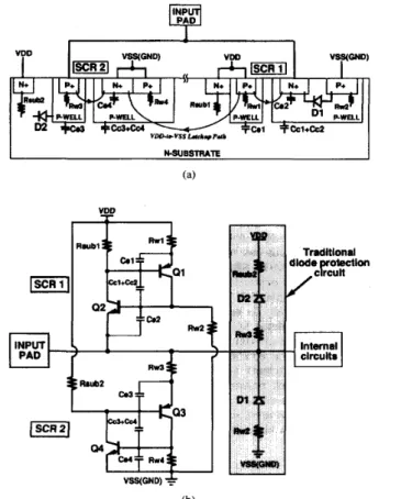
The schematic cross-sectional view of the complementary SCR structures is shown in Fig. l(a), where the n-substrate p - well CMOS process is used to demonstrate the complementary SCR structures. The corresponding lumped equivalent circuit of complementary SCR structures is shown in Fig. l(b). There are two lateral SCR structures in this CSCR ESD protection circuit. The SCRl device is arranged between VDD and input pad with its anode connected to VDD. The SCR2 device is arranged between input pad and VSS(GND) with its anode connected to the pad. The SCRl (SCR2) device is basically formed by the parasitic lateral p-n-p bipolar junction transistor (BJT) Q1 (Q3) and parasitic vertical n-p-n BJT Q2 (Q4). Q 1 and Q3 are parasitic lateral p-welvn-substratelp-well BJT’s,
whereas Q2 and Q4 are parasitic vertical N + diffusiodp- welYn-substrate BJT’s. In lateral p-n-p BJT Q 1 (Q3), p-well instead Of P + diffusion is used as its emitter to make a deeper anode structure for lateral SCRl (SCR2) device. The deeper anode can allow higher current flowing capability to bypass ESD currents so as to increase its ESD failure threshold.
In the complementary SCR structures, there also exist two junction diodes 01 and 0 2 . These two junction diodes are merged into the base-emitter junctions of BJT’s Q2 and Q3 to save layout area. The diode 0 1 is formed by an N + diffusion in a p-well, whereas the diode 0 2 is formed by a p-well in n-substrate.
The parasitic resistances and capacitances in complemen- tary SCR structures are also shown in Fig. l(a) and (b). R w l , Rw2, Rw3, and Rw4 represent p-well inherent resis- tances. Rsubl and Rsub2 are substrate inherent resistances. C e l , C c l
+
Cc2, Ce3, and Cc3+
Cc4 are p-wellln-substrate junction capacitances. Ce2 and Ce4 are N + diffusionlp- well junction capacitances. These capacitances have important effects to lower the ESD-trigger voltage of lateral SCR device 1131, [14l.The cross-sectional view and lumped equivalent circuit shown in Fig. l(a) and l(b) are the implementation of this CSCR ESD protection scheme by a n-substratelp-well CMOS process. This CSCR ESD protection scheme can also be implemented in a psubstrateln-well CMOS process as well if appropriate modifications are made.
IEEE TRANSACTIONS ON ELECTRON DEVICES, VOL. 42, NO. 7, JULY 1995
@
I I
N-SUBSTRATE
-
(b)
Fig. 1. (a) The schematic cross-sectional view of the CSCR ESD protection circuit. (b) The lumped equivalent circuit of the CSCR ESD protection circuit.
B. Operating Principles
In normal CMOS operations with 5-V VDD and 0-V VSS(GND), diodes 0 1 and 0 2 have a voltage-clamping effect on input signals. The input voltage level is limited approximately between -0.6 V and +5.6 V. The lateral SCRl and SCR2 devices under normal operating conditions are in their high-impedance (off) states. Although diode 01 ( 0 2 ) is merged into the emitter of BJT Q2 (Q3) in lateral SCRl (SCR2) device, the current flowing path through diode 0 1 (D2) and that through SCRl (SCR2) device in the cross- sectional view of Fig. l(a) are different. So, if diode 0 1 ( 0 2 ) is forwardly conducting due to input signals undershooting (overshooting) to clamp input voltage level on the pad, the lateral SCRl (SCR2) device is still not triggered on by the forward-biased diode 0 1 ( 0 2 ) .
In ESD stress conditions, there are four ESD-stress cases at the input pad with positive or negative polarities to VDD or VSS(GND). In NS-mode (PD-mode) ESD stress, diode 0 1 ( 0 2 ) is forwardly conducting to bypass ESD current but SCR2 (SCR1) device is off. On the contrary, SCR2 (SCR1) device is triggered on to bypass ESD current but 0 1 ( 0 2 ) diode is off in PS-mode (ND-mode) ESD stress. The lateral SCR2 (SCRI) device is designed to be triggered on before breakdown of diode D1 ( 0 2 ) during ESD transitions. Because diodes 0 1 and 0 2 are not arranged to perform ESD
KER AND WU: COMPLEMENTARY-SCR ESD PROTECTION CIRCUIT VDD
T
SCRl andD1 cl 1299 SCR2 and D 2 k-
J C P VSS~GND)Fig. 2. The lumped equivalent circuit of the VDD-to-VSS latchup path.
protection in their reverse-biased breakdown conditions during ESD transitions, the ESD protection capability of this proposed ESD protection circuit can be improved significantly within a small layout area.
C. VDD-to- VSS Latchup Consideration
There is a parasitic VDD-to-VSS latchup path in the CSCR ESD protection circuit, which is also shown in Fig. l(a). The corresponding lumped equivalent circuit of this VDD-to-VSS latchup path is shown in Fig. 2. In Fig. 2, the parasitic vertical Q4 transistor is the same of BJT Q4 in SCR2 structure. But, the parasitic lateral Q 5 transistor is formed by the p-well emitter of BJT Q1 in SCRl device as its emitter, long-distance n-substrate as its base, and the p-well base of BJT Q4 in SCR2 device as its collector. If SCRl and SCR2 devices are separated by the metal bonding pad in layout, Q 5 transistor will have a very small beta gain due to its long-distance base width. The beta gain of vertical Q4 transistor is also dependent on its base width which is the difference between the depths of p-well and N + diffusion in CMOS technology. In submicron CMOS technologies, the beta gain of parasitic vertical BJT is ordinarily as high as 100
-
200. With such a high beta gain in vertical BJT Q4, VDD-to-VSS latchup may occur if resistances Rsubl and Rw4 are large enough.In order to avoid VDD-to-VSS latchup, the base-emitter shorting method [32], [33] is adopted to reduce the shunt resistances Rsubl and Rw4. In Fig. 2, the base-emitter short- ing effect is presented by the dashed lines shunting across resistances Rsubl and Rw4. If Rsubl (Rw4) is small enough, the base-emitter voltage of BJT
Q5
(Q4) will be hardly triggered above its tum-on voltage as a transient current in the n-substrate @-well). The smaller Rsubl and Rw4 lead to higher holding voltage of VDD-to-VSS latchup path [32]. Rsubl can be significantly reduced by putting an N+ diffusionwith n-substrate bias of 5 V close to the p-well emitter of BJT Q5. Similarly, Rw4 can be reduced by putting a P f diffusion
with p-well bias of 0 V close to the N + diffusion emitter
of BJT Q4. With base-emitter shorting layouts in BJT’s Q4 and Q S as shown in the cross-sectional view of Fig. l(a), the
f For FigA(a)
*
For Flg.qb) Fig. 3. circuit.The interdigitated finger-type layout of the CSCR ESD protection
holding voltage of VDD-to-VSS latchup can be increased to above 5 V. Thus, this proposed CSCR ESD protection circuit can be free of VDD-to-VSS latchup.
111. LAYOUT OF THE CSCR ESD PROTECTION CIRCUIT
A. Interdigitated b y o u t Style of Complementary SCR Structures
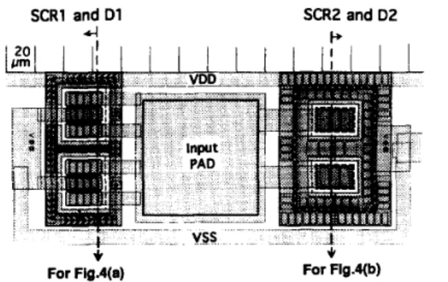
Like the layout style of a CMOS output buffer, interdigitated finger-type layout style is used to implement this CSCR ESD protection circuit. The interdigitated finger-type layout can offer more ESD current discharging paths than that of parallel strip-line style to avoid current crowding effect in the anode areas of lateral SCRl and SCR2 devices as well as to avoid electromigration in metal lines and contacts. A demonstrated layout is shown in Fig. 3 with the corresponding cross-sectional views shown in Fig. 4(a) and (b). In Fig. 3, there are four metal fingers from input pad to the left-hand side to form lateral SCRl and D1 devices, whereas there are two metal fingers from input pad to the right-hand side to form lateral SCR2 and 0 2 devices.
In Fig. 4(a), the cathode of SCRl device is the A-+ diffusion connected to input pad in a VSS-biased p-well which is surrounded by the adjacent VDD-connected p-well anode of SCRl device. The diode D1 is formed by a P+ diffusion
connected to VSS in the center of the p-well where the cathode of SCRl device is in the same p-well. An N + diffusion in n-
substrate closed to the p-well anode of SCRl device is made to surround whole SCRl device. This N + diffusion is also
connected to VDD to offer n-substrate bias.
In Fig. 4(b), the anode of SCR2 device is formed by the P f diffusion in a p-well which is surrounded by its cathode of an
N + diffusion connected to VSS in the adjacent VSS-biased p-
well. The P+ diffusion closed to the A + diffusion cathode of SCR2 device in the adjacent p-well is made to surround whole SCR2 device. This P+ diffusion is also connected to VSS to
offer p-well bias. An N + diffusion connected to VDD in n- substrate, which is placed in the outside of SCR2 device and surrounds SCR2 device, offers the substrate bias and forms the cathode of diode 0 2 . This N + diffusion also works as
IEEE TRANSACTIONS ON ELECTRON DEVICES, VOL. 42. NO. 7, JULY 1995
@
InputI N-SUBSRUTE
I
(b)
Fig. 4. The corresponding cross-sectional view of (a) the lateral SCRl device and diode D1; (b) the lateral SCR2 device and diode 0 2 , in the layout of
Fig. 3.
a guard ring to prevent VDD-to-VSS latchup. The anode of diode 0 2 is the same p-well anode of SCR2 device.
The parasitic VDD-to-VSS latchup path in this interdigitated finger-type layout is from the anode of SCRl device through long-distance n-substrate under input pad to the cathode of SCR2 device. By means of base-emitter shorting layout on resistances Rsubl and Rw4, which are the VDD-connected N + diffusion close to and surrounding the p-well anode of SCRl device as well as the VSS-connected P + diffusion close to and surrounding the N + diffusion cathode of SCR2 device
in Figs. 3 and 4, the VDD-to-VSS latchup path is repeatedly
broken and guarded. The holding voltage of VDD-to-VSS latchup in this layout is expected to be above 5 V.
B. P-Well to P-Well Spacing
Due to base-emitter shorting effect in the VDD-to-VSS latchup path, the resistances of Rsubl and Rw4 are reduced significantly. Reducing the resistances of Rsubl and Rw4 also reduces the latching capability of lateral SCRl and SCR2 devices in the ESD protection circuit. The junction capaci- tances in lateral SCRl and SCR2 devices also provide transient currents to trigger on the lateral SCR devices during ESD transitions 11 31, 1141. But the base-emitter shorting technique on Rsubl (Rw4) also degrades the transient triggering effect of Gel (Ge4) capacitance in SCRl (SCR2) device during ESD transitions. To increase the latching capability of SCRl and SCR2 devices in the CSCR ESD protection circuit, the p-well to p-well spacings of lateral BJT's Q1 and Q3 can be reasonably shortened to increase their beta gains. The shorter p-well to p-well spacing could also lead to punchthrough between two adjacent p-wells before the p-well n-substrate breakdown in SCRl and SCR2 devices. Thus, the trigger
SCRl
and
D1
SCR2 and
02
Fig. 5. A microphotograph of the fabricated CSCR ESD protection circuit. voltage of lateral SCRl and SCR2 devices can be more reduced.
To experimentally investigate the effect of p-well to p-well spacing on the lateral SCRl and SCR2 devices, this spacing on pattem layout varies from 1.2 pm to 3.0 pm with a step of 0.1 or 0.2 pm in the test chip.
IV. EXPERIMENTAL RESULTS
Using the interdigitated finger-type layout in Fig. 3, the CSCR ESD protection circuit with one set of different p - well to p-well spacings is fabricated by a 0.6-pm twin-well n-substrate CMOS SRAM technology with modified LDD structure 1341. The thickness of gate oxide in PMOS or NMOS devices is 150
A.
The spacing of N + diffusion inside p-wellto the p-well edge is 2.8 pm. The layout area of lateral SCRl device with D1 diode is 108 x 44 pm2. The layout area of SCR2 device with 0 2 diode is 108 x 76 pm2 which includes a surrounding N + diffusion as latchup guard ring with ring width of 10 pm. A microphotograph of fabricated CSCR ESD protection circuit with p-well to p-well spacing of 2.0 pm is shown in Fig. 5.
A. VDD-to- VSS Latchup Characteristics
With 10-pm N + diffusion guard ring and the base-emitter
shorting technique, the dc I-V characteristics of VDD-to-VSS latchup path in the fabricated CSCR ESD protection circuit is shown in Fig. 6 with p-well to p-well spacing of 1.6 pm. It is shown that the dc holding voltage is as high as 17.5 V, which is much greater than the 5-V VDD power supply. In the fabricated CSCR ESD protection circuits with different p -
well to p-well spacings, the holding voltage of VDD-to-VSS latchup path is around 16
-
18 V. Thus, the proposed CSCR ESD protection circuit has been experimentally verified to be free of VDD-to-VSS latchup. The dc holding current in Fig. 6 is 16.5 mA and the dc switching voltage (current) is 44.15 V (1 1.75 mA).KER AND WU: COMPLEMENTARY-SCR ESD PROTECTION CIRCUIT 1.15 1.10 1.05 1.00 VERT/DIV SnA cumm 16.5O.A HORIZ/OIV 5 v CURSOR 17.50 V PER STEP 50nA OFFSET 0.om B o r gn/01v 110.K X O F CLILLECTOR PEAK VOLTS 7 5 . 4 AUX SUPPLY
-
-
-
-
TYPE 9704 0.00 v ... ~ Fig. 6.protection circuit with y-well to p-well spacing of 1.6 I'm.
The dc I-V characteristics of VDD-to-VSS latchup in the CSCR ESD
Fig. 7. The measured I-V characteristics of the lateral SCRl device in the fabricated CSCR ESD protection circuit with p-well to p-well spacing of 1.4 pm, which is measured from VDD node to input pad with VSS node floating.
B. Turn-on Characteristics of Complementary SCR Structures
The dc I-V characteristics of fabricated lateral SCRl device with its p-well to p-well spacing of 1.4 pm is shown in Fig. 7 with turn-on resistance of 1.7 0, which is measured from VDD node to input pad with VSS node floating. The dc switching voltage (current) and holding voltage (current) are 12.92 V (1.34 mA) and 0.996 V (5.22 mA), respectively. The relation between the dc switching voltage (current) and the p-well to p-well spacing in lateral SCRl device is shown in Fig. 8(a). The relation between the holding voltage (current) and the p-well to p-well spacing is shown in Fig. 8(b). It is shown that the dc switching voltage keeps around 30 V due to p- wellln-substrate junction breakdown when the p-well to p-well spacing is greater than 1.6 pm. But, the dc switching voltage nearly linearly decreases as the p-well to p-well spacing is less than 1.6 pm. The critical p-well to p-well spacing in this 0.6-pm CMOS technology to cause punchthrough is 1.6 pm. The dc switching voltage is lowered to 1.1 16 V when the spacing is only 1.2 pm, which is too low for the application
1301 16
l a
' W
I-
is
/i.l-
P
1.2 1.4 1.6 Switching Current n P-Well to P-Well Spacing (pm)(a)
0.95' . ' . ' . ' . ' . ' . ' . ' . ' ' ' . 14
1.0 1.2 1.4 1.6 1.0 2.0 2.2 2.4 2.6 2.0 3.u P-Well to P-Well Spacing (pm)
(b)
Fig. 8. The relations between (a) the dc switching voltage/current; (b) the holding voltage/current, and the p-well to p-well spacing in lateral SCRl device.
in 5-V CMOS circuits. In Fig. 8(b), the holding voltage is around 0.986 V to 1.112 V with the spacing from 1.2 p m to 3.0 pm. With such low holding voltage, the ESD voltage at input pad can be clamped to a very low voltage level without damaging internal circuits. The turn-on resistance of lateral SCRl device is around 1.6 to 2.0 R for the p-well to p-well spacing from 1.2 to 3.0 pm. With such low turn-on resistance in high-current range, the CSCR ESD protection circuit can provide very efficient discharging path to bypass ESD stresses. With the same structure as lateral SCRl device, the turn-on characteristics of lateral SCR2 device are similar to those of SCRl device.
The junction capacitances in lateral SCR device can provide transient currents to turn on itself during ESD transitions. Thus, the ESD-trigger voltage of lateral SCR device is lower than its dc switching voltage due to transient effect in device capacitance [ 141. To investigate the ESD-trigger voltage of lateral SCR device with different p-well to p-well spacings, a pulse-type voltage waveform with 5-nS rise time and 20- pS pulse width generated by a HP81 16A pulse generator is applied to the anode of lateral SCRl device with its cathode grounded. The results are shown in Fig. 9. It is shown that the pulse-type trigger voltage of lateral SCR device is about 9.02 V when the spacing is 1.4 pm, and the pulse-type trigger
1302 IEEE TRANSACTIONS ON ELECTRON DEVICES, VOL. 42, NO. 7, JULY 1995
P-Well to P-Well Spacing (pm) Fig. 9.
device and the p w e l l to p-well spacing.
The relations between the pulse-type trigger voltage of lateral SCR
voltage slightly increases to about 1 1.78 V when the p-well to p-well spacing increases to 3.0 pm. This implies an important design guideline that the p-well to p-well spacing should be chosen so that the SCR devices are triggered on by the pulse-type voltage triggering rather than by the breakdown or punchthrough between the two p-wells. This can guarantee an excellent reliability of the proposed CSCR ESD protection circuits. With a low pulse-type trigger voltage, the lateral SCR device can be quickly turned on to bypass ESD current before ESD damaging internal circuits. Although the base-emitter shorting technique on resistors Rsubl and Rw4 used to avoid VDD-to-VSS latchup also degrades the transient currents of Cel and Ce4 in lateral SCRl and SCR2 devices, the pulse- type trigger voltage of lateral SCRl and SCR2 devices can still be lowered from the dc switching voltage about 30 V to only around 10
-
11 V as shown in Figs. 8(a) and 9. Thus, with the interdigitated finger-type layout style and the base- emitter shorting method, the CSCR ESD protection circuit can offer effective low ESD-trigger voltage and also be free of VDD-to-VSS latchup.Moreover, to show that the SCRl and SCR2 devices are not triggered on in the high-speed CMOS operations, a voltage pulse string with the pulse width varying from 10 nS to 5 mS, high level voltage above 5.6 V, low level voltage below -0.6 V, and the rise time around 200 pS generated by a HP8131A 500 MHz pulse generator is applied to the input pad of fabricated ESD protection circuit with 5-V VDD and grounded VSS. The voltage pulse string does not trigger on the lateral SCRl and SCR2 devices in the fabricated ESD protection circuit, because the voltage level on the pad with overshootinghndershooting input signals is clamped to -0.6
-
+
5.6 V by diodes Dl and 0 2 . Thus the lateral SCRl and SCR2 devices are not triggered on by high-speed operating input signals with overshootinghndershooting conditions.C. ESD Testing Results
The fabricated complementary-SCR ESD protection circuit with different p-well to p-well spacings are tested by both Human-Body-Mode (HBM) ESD and Machine-Mode (MM) ESD. The ESD voltage pulses have positive and negative polarities with respect to VDD and VSS nodes. For each p-well
to p-well spacing, there are at least five samples of fabricated CSCR ESD protection circuits to be tested under each ESD- stress mode of both HBM and MM ESD. The minimum ESD failure voltage of the tested five samples is adopted as the ESD failure threshold of ESD protection circuit. The HBM and MM ESD testing results are shown in Fig. 10(a) and (b), respectively. The ESD failure criterion is defined as the initial voltage of l-pA current leakage shifting 40% after ESD stress. In Fig. lO(a), it is seen that the HBM ESD failure threshold from input pin to VSS can be above 5 10 KV if the p-well
to p-well spacing below 1.8 pm, whereas that from input pin to VDD is above f 7000 V. In Fig. 10(b), it is shown that the MM ESD failure threshold from input pin to VSS node can be above f l KV if the p-well to p-well spacing below 1.8 pm, whereas that from input pin to VDD is above *400 V. When the p-well to p-well spacing of lateral SCR device increases from 1.8 to 3.0 p m , both HBM and MM ESD failure thresholds in Figs. 10(a) and 10(b) roughly decrease to about
f 5000 V and f 250 V, respectively. The shorter p-well to p-well spacing in lateral SCR devices provides higher beta gains of lateral pn-p BJT's Q1 and Q3, which causes stronger
positive-feedback regeneration and leads to quicker turn-on in the lateral SCR devices to bypass the sudden ESD stresses. Thus, the CSCR ESD protection circuit with shorter p-well to p-well spacing provides submicron CMOS IC's with higher ESD protection capability.
As seen in Figs. 10(a) and (b), the ESD failure threshold from input pin to VSS is almost higher than that from input pin to VDD under the same p-well to p-well spacing. The reason why the lateral SCRl and SCR2 devices have the same p-well to p-well spacing but different ESD failure thresholds are due to the layout of cathode in SCRl device. As seen in Fig. 3,
the SCR2 device is fully surrounded by its cathode connected to VSS node, but the SCRl device is partially surrounded by its anode connected to VDD node. The cathode of lateral SCRl device is also the cathode of diode D l as shown in Fig. 4(a). To improve the ESD failure threshold from input pin to VDD, the cathode of lateral SCRl dekice should be fully surrounded by its VDD-connected p-well anode whereas the VSS-connected P+ diffusion anode of diode D1 should
be placed in the center of the p-well and surrounded by the
N f diffusion cathode of SCRl device.
V. CONCLUSION
A robust ESD protection circuit with complementary SCR structures and junction diodes has been designed and fabri- cated by a 0.6-pm CMOS SRAM technology. The VDD-to- VSS latchup issue in the ESD protection circuit has been overcome by means of base-emitter shorting method. The experimental results show that the dc holding voltage of VDD- to-VSS latchup can be increased up to 17.5 V. The p-well to p-well spacing in the lateral SCR devices is reduced to lower the pulse-type ESD trigger voltage and to enhance turn-on speed of positive-feedback regenerative process in the lateral SCR devices. ESD testing results show that an input pad with the CSCR ESD protection circuit under p-well to p-well spacing below 1.8 p m can sustain above k7000 V human-
KER AND W U COMPLEMENTARY-SCR ESD PROTECTION CIRCUIT 1303
-
-
-1-
-
- -
L
(Ilmlod b ESDE
test machrns)[2] C. Duvvury, T. Taylor, J. Lindgren, J. Moms and S. Kumar, “Input protection design for overall chip reliability,” in EOYESD Symp. froc., [3] C. Duvvury and R. Rountree, “A synthesis of ESD input protection
scheme,” in EOS/ESD Symp. Proc., vol. EOS-13, pp. 88-97, 1991. [4] B. Carbajal In, R. Cline and B. Andresen, “A successful HBM ESD
protection circuit for micron and sub-micron level CMOS,” EOS/ESD
Symposium Proc., vol. EOS-14, pp. 234-242, 1992.
[5] K. L. Chen and R. H. Pang, “Electrostatic discharge protection for semiconductor input devices,” United States Patent 5077591, Dec. I99 I. [6] A. Chatterjee and C. Duvvury, “Efficient ESD input protection scheme,”
United States Patent 4896243, Jan. 1990.
[7] R. N. Rountree, “Electrostatic discharge protection circuit,” United States Patent 5012317, Apr. 1991.
[8] K. D. Chen and R. H. Pang, “Method of making electrostatic dis- charge protection for semiconductor input devices,” United States Patent vol. EOS-11, pp. 190-197, 1989. A ’ .bove1oooov
f
gooo a 0 u s h.-.*.. 0 0 8wo-
4.. a... ’ a . . A-. ... & a . . . -. k z m -Elf!
w 4 o o o ~ ” ” ” ” ” ” ” ” ” ’ 1.2 1.4 1.6 1.8 2 . 0 2.2 2.4 2.6 2.8 3.0 3.2P-Well to P-Well Spacing (pm) (a)
I \ I
5166089, Nov. 1992.
[9] G. Rieck and R. Manely, “Novel ESD protection for advanced CMOS output drivers,” in EOS/ESD Symp. Pmc., vol. EOS-1 I, pp. 182-189, 1989.
[IO] R. N. Rountree, “Circuit structure with enhanced electrostatic discharge protection,” United States Patent 4939616, July 1990.
[ l I] A. Chatterjee and T. Polgreen, “A low-voltage triggering SCR for on- chip ESD protection at output and input pads,” in Proc. Symposium on
VLSI Technology, pp. 75-76, 1990.
[12] -, “A low-voltage triggering SCR for on-chip ESD protection at output and input pads,” IEEE Electron Device Lett., vol. 12, no. 1, pp. 21-22, Jan. 1991.
[13] C.-Y. Wu, M.-D. Ker, C.-Y. Lee and J. KO, “A new on-chip ESD protection circuit with dual parasitic SCR structures for CMOS VLSI,”
IEEE J. Solid-Stare Circuits, vol. 27, no. 3, pp. 274-280, Mar. 1992.
[14] M.-D. Ker, C.-Y. Wu and C.-Y. Lee, “A novel CMOS ESDEOS protection circuit with full-SCR structures,” EOSIESD Symposium Proc., [15] M.-D. Ker, C.-Y. Lee, C.-Y. Wu and J. KO, “CMOS ESD protection
circuit with parasitic SCR structures,” United States Patent 5140401, vol. EOS-14, pp. 258-264, 1992.
Aug. 1992.
1.2 1 . 4 1.6 l.* 2.0 2.2 2.4 2.6 2 . 6 3 - 0 3.2 1161 M.-D. Ker, C.-Y. Lee and C.-Y. Wu, “CMOS on-chip ESD protection
P-Well to P-Well Spacing (pm) circuit and semiconductor structure,” U.S. Patent 5 182220, Jan. 1993; also U.S. Patent 5289334. Feb. 1994.
(b) [17] S. Shabde, G . Si&ons, A. Balun1 and D. Back, “Snapback induced gate dielectric breakdown in graded junction MOS structhes,” in Pmc.
of IRPS, pp. 165-168, 1984.
[I81
c,
D ~R. R ~ ~D, ~ ~ ~~~R, ~~~~~ p~,A, ~~~l~~ and lh ~~~~ ~,L, , , White, “ESD design considerations for ULSI,” EOS/ESD SymposiumFig. IO. The dependence of (a) the human-body-mode; (b) the ma- chine-mode, ESD failure threshold of the fabricated CSCR ESD protection circuit on the p-well to p-well spacing in lateral SCR devices.
Proc., vol. EOS-7, pp. 45-48, 1985.
[I91 R. McPhee, C. Duvvury, R. Rountree and H. Domingos, “Thick ox- ide ESD performance under process variations,” EOVESD Symposium
Proc., vol. EOS-8, pp. 173-181, 1986.
[20] K. L. Chen, G . Giles and D. B. Scott, “Electrostatic discharge protection for one micron CMOS devices and circuits,” IEDM Tech. Dig., pp. 484-487. 1986.
body-mode and f400 V machine-mode ESD stresses within a small layout size. In normal CMOS operating conditions with 5-V VDD power supply, diodes 01 and 0 2 in the CSCR ESD protection circuit also offer voltage clamping effect to limit the I
- -
input voltage level between -0.6 V N +5.6 V.
This proposed complementary-SCR ESD protection circuit can provide submicron CMOS IC’s with direct and effective ESD discharging paths from the input pad to both VDD and VSS power lines. Thus, the unexpected ESD damages on the internal circuits beyond ESD protection circuits can be avoided.
ACKNOWLEDGMENT
The authors wish to thank Chung-Yuan Lee and Joe KO of United Microelectronics Corporation, Taiwan, for their helps on chip fabrication and ESD testing. Thanks are also due to the associate editor, Dr. Kunio Tada, and his reviewers for their valuable suggestions to revise this paper.
REFERENCES
[ l ] R. N. Rountree, C. Duvvury, T. Maki and H. Stiegler, “A process- tolerant input protection circuit for advanced CMOS processes,” in
EOYESD Symp. Proc., vol. EOS-IO, pp. 201-205, 1988.
[21] C. Duvvury, R. McPhee, D. Baglee and R. Rountree, “ESD protection reliability in 1 p m CMOS technologies,” froc. of IRPS, pp. 199-205,
1986.
[22] D. B. Scott et al., “Titanium silicide contact resistivity and its impact on I-pm CMOS circuit performance,” IEEE Trans. Electron Devices, vol. 34, no. 3, pp. 562-574, 1987.
[23] R. Rountree, “ESD protection for submicron CMOS circuits: Issues and solutions,” IEDM Tech. Dig., pp. 58@583, 1988.
[24] K. L. Chen, “The effects of interconnect process and snapback voltage on the ESD failure threshold of NMOS transistors.” IEEE Trans.
Electron Devices, vol. 35, no. 12, pp. 214&2150, 1988.
[25] C. Duvvury, R. Rountree, H. Stiegler, T. Polgreen and D. Corum, “ESD phenomena in graded junction devices,” froc. of IRPS. pp. 71-76, 1989. [26] A. Amerasekera, L. Roozendaal, J. Abderhalden, J. Bruines and L. Sevat, “An analysis of low voltage ESD damage in advanced CMOS processes,” in EOS/ESD Svmp. froc., vol. EOS-12, pp. 143-150, 1990. [27] C. Duvvury and A. Amerasekera, “ESD: A pervasive reliability concern for IC technologies,” in Pmc. of IEEE, vol. 81, no. 5 , pp. 690-702, May 1993.
[28l C. Duvvury, R. N. Rountree and 0. Adams, “Internal chip ESD phe- nomena beyond the protection circuit,” IEEE Trans. Electron Devices, vol. 35, no. 12, pp. 2133-2139, Dec. 1988.
[29] H. Terletzki, W. Nikutta and W. Reczek, “Influence of the series resistance of on-chip power supply buses on internal device failure after ESD stress,” IEEE Trans. Electron Devices, vol. 40, no. 11, pp. 2081-2083, NOV. 1993.
1304 IEEE TRANSACTIONS ON ELECTRON DEVICES, VOL. 42, NO. 7, JULY 1995
[30] C. Johnson, T. J. Maloney and S. Qawami, “Two unusual HBM ESD failure mechanisms on a mature CMOS process,” EOS/ESD Symposium Proc., vol. EOS-15, pp. 225-231, 1993.
[31] X. Guggenmos and R. Holzner, “A new ESD protection concept for VLSI CMOS circuits avoiding circuit stress,” EOS/ESD Symposium Proc., vol. EOS-13, pp. 74-82, 1991.
[32] R. R. Troutman, Latchup in CMOS Technology: The Problem and Ifs Cure, Kluwer Academic Publishers, USA, 1986.
[33] A. Blicher, Thyrisfor Physics. New York Springer-Verlag, 1976. [34] J. W. Chou, C. Y. Chang and J. KO, “A new surface counter doped LDD
(SCD-LDD) structure for deep submicron (0.35 pm) MOSEETs,” in
proc. Inr. sJ”P. vLsI sYsfem, and APPzicutions* Taiwan,
pp 178-181, 1993.
Chung-Yu Wu was bom in Chiayi, Taiwan, Repub- lic of China, in 1950. He received the B.S. degree from the Department of Electrophysics, and the M.S. and Ph.D. degrees from the Institute of Elec- tronics, National Chiao-Tung University, Hsinchu, Taiwan, in 1972, 1976, and 1980, respectively.
From 1975 to 1976, he studied ferroelectnc films on silicon and their device applications, and from 1976 to 1979 he engaged in the development of integrated differential negative resistance devices and their circuit applications, with support from the National Electronics Mass Plan (Semiconductor Devices and Integrated Circuit Technologies) of the National Science Council. From 1980 to 1984, he was an Associate Professor at the Institute of Electronics, National Chiao- Tung University. From 1984 to 1986, he was an Associate Professor in the Department of Electrical Engineering, Portland State University, Portland, OR. Ming-Dou Ker was bom in Taiwan, Republic of
China, in 1963. He received the B.S degree from the Department of Electronics Engineenng, and the M.S. and Ph.D. degrees from the Institute of Elec- tronics, National Chiao-Tung University, Hsinchu. Taiwan, in 1986, 1988, and 1993, respectively.
From 1986 to 1988, he studied the timing models of CMOS integrated circuits, and from 1989 to 1993, he engaged in the development of CMOS on-chip ESD protection circuits and CMOS latchup analysis, with support from the United Microelec- tronics Corporation (UMC), Tawan. From 1993 to 1994 he was a postdoctoral researcher in Integrated Circuits and Systems Laboratory, Institute of Electron- ics, National Chiao-Tung University, Hsinchu, Taiwan. In 1994, he joined the VLSI Design Department of Computer & Communication Research Laborato-
ries (CCL), Industrial Technology Research Institute (ITRI), Hsinchu, Taiwan, as a circuit design engineer. Since then he was engaged in the development of mixed-mode integrated circuits in submicron CMOS technology. His research interests include reliability of CMOS integrated circuits, nuxed-mode integrated circuits, and communication integrated circuits design.
Dr. Ker is a member of ESD Association
Presently, he is a professor in the Department of Electronics Engineering and Institute of Electronics, National Chiao-Tung University. He has published more than 60 journal papers and 80 conference papers on several topics, including digital integrated circuits, analog integrated circuits, computer-aided design, ESD protection circuits, special semiconductor devices, and process technologies. He has 9 patents, including 5 U.S. patents. His current research interests focus on low voltage mixed-mode integrated circuit design, hardware implementation of visual and auditory neural systems, and RF integrated circuit design.