國
立
交
通
大
學
電機學院 電機與控制學程
碩
士
論
文
離子感測場效電晶體對於溫度及閘極電壓應力調變之可靠度研究
The study of ISFET’s reliability with temperature and
gate voltage stress modulation
研 究 生:黃明欽
指導教授:張國明 教授
蘇朝琴 教授
離子感測場效電晶體對於溫度及閘極電壓應力調變之可靠度研究
The study of ISFET’s reliability with temperature and
gate voltage stress modulation
研 究 生:黃明欽 Student:Ming-Chin Huang
指導教授:張國明 Advisor:Kow-Ming Chang
蘇朝琴 Chau-Chin Su
國立交通大學
電機學院 電機與控制學程
碩士論文
A Thesis
Submitted to College of Electrical and Computer Engineering
National Chiao Tung University
in partial Fulfillment of the Requirements
for the Degree of
Master of Science
in
Electrical and Control Engineering
September 2007
Hsinchu, Taiwan, Republic of China
中華民國九十六年九月
離子感測場效電晶體對於溫度及閘極電壓應力調變之可靠度研究
學生:黃明欽 指導教授:張國明 博士
蘇朝琴 博士
國立交通大學 電機學院 電機與控制學程碩士班
摘 要
離子感測場效電晶體最初是由 P.Bergveld 在 1970 年代所提出來的一種化學感測 器,主要是利用金屬半導體場效電晶體(MOSFET)的原理,ISFET 與 MOSFET 不同的是將離 子感應層(Ion Sensitive Layer) 、酸鹼緩衝溶液(pH Buffer Solutions) 和一外加之 參考電極取代 MOSFET 之金屬閘極,ISFET 的電性特性將會隨著離子感應層與溶液的表 面接觸性質而改變。 此研究是以四種與 CMOS 製程相容的材料作為閘極感應層對於標準溶液進行探討。 元件的所有製程均在國家奈米實驗室與國立交通大學奈米中心的一萬級無塵室中進行 與完成。所有量測過程是利用 HP4156 儀器並且在黑箱中進行。在不同的溫度條件下對 於不同緩衝溶液的 pH 值測其汲極電流與閘極電壓的曲線,藉由不同的汲極電流與閘極 電壓曲線來定義靈敏度。為了尋求最佳的穩定條件,使用閘極電壓調變量來找出可靠度 與酸離子之間的關係。 此篇論文將詳述離子感測器的製作流程及量測條件。在本研究裡有四個研究項目, 溫度變化下的靈敏度、閘極對電壓應力調變的影響、溫度的遲滯效應以量測再現性。The study of ISFET’s reliability with temperature and
gate voltage stress modulation
Student: Ming-Chin Huang Advisor: Dr. Kow-Ming Chang
Dr. Chau-Chin Su
Degree Program of Electrical and Computer Engineering National Chiao Tung University
Abstract
The ion-sensitive field effect transistor (ISFET) is a chemical sensor that was first presented by P. Bergveld in 1970. The main point is used Metal Oxide Silicon Field Effect Transistor (MOSFET) principium. The ISFET is different with MOSFET on the metal gate of MOSFET which was replaced by an ion-sensitive layer, buffer solutions, and an additional reference electrode. The electrical characteristics of ISFETs will vary with the interface reactions of sensing layer and electrolyte solution.
In this study, four CMOS fabrication compatible membranes were used to be the sensing layers on ISFETs. All processes of the devices were completed in the clean room (class 10000) of NDL and NFC in NCTU. All measuring processes was in a dark box using HP4156A semiconductor parameter analyzer. The devices were soaked in buffer solutions to get the ID_VG curves with varied temperatures and pHs. The sensitivities were defined by the disparities of ID_VG curves. In order to seek the optimum stabilization conditions, a gate voltage stress modulation was used to find the relations of reliability and acid ion.
In this thesis, we will describe details on fabrication process flow and measurement conditions. In this study, there are four researches in sensitivities of varies temperature, the
誌 謝
首先,我要感謝張國明及蘇朝琴老師在我碩士班期間給予我的指導與教誨,使我在 半導體元件以及製程相關知識與技術上成長許多,並在研究分析論文或是待人處事等方 面都獲得莫大的助益。 其次,感謝奈米中心及國家奈米實驗室全體人員在實驗過程中的協助,使我可以順 利進行我的實驗。並且特別感謝諸位口試委員的蒞臨指導,讓我在口試過程中對於我的 研究有新的體認,相信對於以後的研究有莫大的幫助。 再者,感謝張知天學長與趙高毅學長,在實驗過程中不斷的給予協助、鼓勵及建議, 並且提供我許多寶貴的經驗,讓我在學習的過程更加順利。還有實驗室的同學周庭緯和 徐信佑,感謝你們的協助與共患難的精神讓我在工作百忙之餘仍能順利完成論文實驗。 此外,還要感謝我在致新科技產品應用部直屬主管胡雲智處長與總經理吳錦川博 士,他們鼓勵我到交大研究所進修並且給予我最大的空間,讓我得以順利完成繁重的課 業並且取得良好的成績。 最後要感謝我的母親與太太瑞貞,因為他們的支持與陪伴,讓我在研究過程中無後 顧之憂及永遠都有新生的力氣,得以順利完成我的碩士論文,謝謝。 誌于 2007. 9 黃明欽Contents
Abstract
(in Chinese)
……….. iAbstract
(in English)
……….. iiAcknowledgement
……….. ivContents
……….. vTable Captions
……….. viiFigure Captions
……….. viiiChapter 1
Introduction
……… 11.1 Motivation of this work………... 1
1.2 Introduction the ISFET………... 1
1.3 Introduction the pH……….. 2
1.4 The pH Detect Technique……… 3
Chapter 2
Theories for the Investigation of ISFET’s
Temperature and Drift Characteristics
……… 42.1 Basic Principles of ISFET..……….………. 4
2.1.1 From MOSFET to ISFET……… 4
2.1.2 The Oxide-Electrolyte Interface of pH Response.…………... 6
2.2 Introduction the Temperature Phenomenon………...….. 7
2.3 Introduction the Drift Phenomenon……...……….. 8
2.3.1 Physical Model for Drift……….. 9
2.3.2 Drift Expression………... 10
Chapter 3
Procedures of the Experiment
……….………. 133.1 ISFET Fabrication Process Flow….………...…. 13
3.2 Experiment details ……….. 14
3.2.1 Gate Region Formation……… 14
3.2.2 Sensing Layer Deposition……… 14
3.3 Measurement System………... 15
3.3.1 Preparation Before Measuring………...….. 15
3.3.2 Measurement Set-Up…...………..……..…… 16
3.3.3 Temperature Measurement Set-Up……….…………. 16
Chapter 4
Results and Discussions
……….. 184.1 Temperature Sensitivities of Various Membranes…………... 18
4.1.1 ZrO2 membrane gate ISFET………..………... 18
4.1.2 Ta2O5 membrane gate ISFET………... 18
4.1.3 Thermal Oxide membrane gate ISFET……….... 19
4.1.4 PE Oxide membrane gate ISFET………..…... 19
4.1.5 Followings are the discussion of the measurement results….. 20
4.2 Drift Characteristics of Gate Stress Voltages in Various Membranes………... 21
4.2.1 ZrO2 membrane gate ISFET……….……... 21
4.2.2 Ta2O5 membrane gate ISFET……….……….. 21
4.2.3 Thermal Oxide membrane gate ISFET……… 21
4.2.4 PE Oxide membrane gate ISFET………. 22
4.3 Drift Characteristics Hysteresis of Cycle Time Test in
Various Membranes………...….. 23
4.3.1 ZrO2 membrane gate ISFET………….………... 23
4.3.2 Ta2O5 membrane gate ISFET………..………. 23
4.3.3 Thermal Oxide membrane gate ISFET……… 23
4.3.4 PE Oxide membrane gate ISFET….…….………... 24
4.3.5 Followings are the discussion of the measurement results….. 24
4.4 Conclusions……….. 24
Chapter 5
Future Work
………... 275.1 Temperature and Gate Voltage Stress Modulation Influence……….. 27
References
……….. 28Author
Biographical note
……….. 97Table Captions
Table 4-1 Sensitivity of the ZrO2, Ta2O5, Thermal Oxide, and PE Oxide gate ISFET in pH=1, 3, 5, 7 buffer solutions at temperatures of 25℃, 35℃, 45℃, 55℃,65℃, 75℃, and 85℃……….. 91 Table 4-2 Normalize the temperature sensitivity of the ZrO2, Ta2O5, Thermal
Oxide, and PE Oxide gate ISFET in pH=1, 3, 5, 7 buffer solutions at temperatures of 25℃, 35℃, 45℃, 55℃, 65℃, 75℃, and 85℃……… 92 Table 4-3 Temperature sensitivity correlation coefficient of the ZrO2, Ta2O5,
Thermal Oxide, and PE Oxide gate ISFET in pH=1, 3, 5, 7 buffer solutions at temperatures of 25℃, 35℃, 45℃, 55℃, 65℃, 75℃, and 85℃………...……….. 92 Table 4-4 Iso-thermal point VG range of the ZrO2, Ta2O5, Thermal Oxide, and
PE Oxide gate ISFET in pH=1, 3, 5, 7 buffer solutions………. 93 Table 4-5 The relation of the ZrO2, Ta2O5, Thermal Oxide, and PE Oxide drift
voltages and gate stress voltages………. 93 Table 4-6 VG vs Cycle time test of the ZrO2gate ISFET in pH=7 buffer solution
at either 25℃ or 85℃……….……… 94 Table 4-7 VG vs Cycle time test of the Ta2O5 gate ISFET in pH=7 buffer
solution at either of 25℃ or 85℃………... 94 Table 4-8 VG vs Cycle time test of the Thermal Oxide gate ISFET in pH=7
buffer solution at either 25℃ or 85℃………. 94 Table 4-9 VG vs Cycle time test of the PE Oxide gate ISFET in pH=7 buffer
solution at either 25℃ or 85℃………... 95 Table 4-10 △VG vs Cycle time test of the ZrO2, Ta2O5, Thermal Oxide, and PE
Oxide gate ISFET in pH=7 buffer solution at either 25℃ or 85℃…… 95 Table 4-11 Cycle time error rate of the ZrO2, Ta2O5, Thermal Oxide, and PE
Oxide gate ISFET in pH=7 buffer solution at either 25℃ or 85℃…… 96 Table 4-12 △VG cycle time error rate of the ZrO2, Ta2O5, Thermal Oxide, and PE
Figure Captions
Figure 2-1 Electrode and electrolyte interface………... 31
Figure 2-2 Schematic representation of (a) MOSFET, (b) ISFET………... 32
Figure 2-3 Schematic representation of the site-binding model………... 32
Figure 2-4 ID-VG characteristic of MOSFET and ISFET in different temperatures. 33 Figure 2-5 ID-VG characteristic of MOSFET in different temperatures…………... 33
Figure 2-6 ID-VG characteristic of ISFET in different temperatures……… 34
Figure 2-7 Series combination of the (a) initial (b) hydrated insulator capacitance 34 Figure 3-1 Corresponding graph for fabricate process flow………. 37
Figure 3-2 Shows the set up of measurement with the HP4156A Semiconductor Parameter Analyzer at room temperature………...………… 37
Figure 3-3 ID-VD curve of the 300Å ZrO2-gate ISFET………. 38
Figure 3-4 ID-VD curve of the 300Å Ta2O5-gate ISFET……….…………. 38
Figure 3-5 ID-VD curve of the 300Å Thermal Oxide-gate ISFET……… 39
Figure 3-6 ID-VD curve of the 300Å PE Oxide-gate ISFET…………...………….. 39
Figure 3-7 Shows the set up of measurement with the HP4156A Semiconductor Parameter Analyzer and temperature controller…………....…………. 40
Figure 3-8 Detection principle of different VG…………. ………... 40
Figure 4-1 ID-VG curves of the ZrO2 gate ISFET in pH=1, 3, 5, 7 buffer solutions at 25℃………. 41
Figure 4-2 Sensitivity of the ZrO2 gate ISFET in pH=1, 3, 5, 7 buffer solutions at 25℃……...…... 41
Figure 4-3 ID-VG curves of the ZrO2 gate ISFET in pH=1, 3, 5, 7 buffer solutions at 35℃…... 42
Figure 4-4 Sensitivity of the ZrO2 gate ISFET in pH=1, 3, 5, 7 buffer solutions at 35℃……... 42
Figure 4-5 ID-VG curves of the ZrO2 gate ISFET in pH=1, 3, 5, 7 buffer solutions at 45℃…... 43
Figure 4-6 Sensitivity of the ZrO2 gate ISFET in pH=1, 3, 5, 7 buffer solutions at 45℃……... 43
Figure 4-7 ID-VG curves of the ZrO2 gate ISFET in pH=1, 3, 5, 7 buffer solutions at 55℃………... 44
Figure 4-8 Sensitivity of the ZrO2 gate ISFET in pH=1, 3, 5, 7 buffer solutions at 55℃……... 44
Figure 4-9 ID-VG curves of the ZrO2 gate ISFET in pH=1, 3, 5, 7 buffer solutions at 65℃………... 45
Figure 4-10 Sensitivity of the ZrO2 gate ISFET in pH=1, 3, 5, 7 buffer solutions at 65℃………... 45
Figure 4-11 ID-VG curves of the ZrO2 gate ISFET in pH=1, 3, 5, 7 buffer solutions at 75℃…... 46
Figure 4-12 Sensitivity of the ZrO2 gate ISFET in pH=1, 3, 5, 7 buffer solutions at 75℃……... 46
Figure 4-13 ID-VG curves of the ZrO2 gate ISFET in pH=1, 3, 5, 7 buffer solutions at 85℃…... 47
Figure 4-14 Sensitivity of the ZrO2 gate ISFET in pH=1, 3, 5, 7 buffer solutions at 85℃……... 47 Figure 4-15 Temperature sensitivity and correlation coefficient dependency of the
ZrO2 gate ISFET………. 48 Figure 4-16 Normalize the temperature sensitivity curve of the ZrO2 gate ISFET… 48 Figure 4-17 ID-VG curves of the ZrO2 gate ISFET in pH=1 buffer solution at
temperatures of 25℃, 35℃, 45℃, 55℃, 65℃, 75℃, and 85℃……… 49 Figure 4-18 ID-VG curves of the ZrO2 gate ISFET in pH=3 buffer solution at
temperatures of 25℃, 35℃, 45℃, 55℃, 65℃, 75℃, and 85℃……… 49 Figure 4-19 ID-VG curves of the ZrO2 gate ISFET in pH=5 buffer solution at
temperatures of 25℃, 35℃, 45℃, 55℃, 65℃, 75℃, and 85℃……… 50 Figure 4-20 ID-VG curves of the ZrO2 gate ISFET in pH=7 buffer solution at
temperatures of 25℃, 35℃, 45℃, 55℃, 65℃, 75℃, and 85℃……… 50 Figure 4-21 Iso-thermal point range of the ZrO2 gate ISFET in pH=1, 3, 5, 7
buffer solutions………... 51 Figure 4-22 ID-VG curves of the Ta2O5 gate ISFET in pH=1, 3, 5, 7 buffer
solutions at 25℃…………...……….. 51 Figure 4-23 Sensitivity of the Ta2O5 gate ISFET in pH=1, 3, 5, 7 buffer solutions
at 25℃………. 52 Figure 4-24 ID-VG curves of the Ta2O5 gate ISFET in pH=1, 3, 5, 7 buffer
solutions at 35℃………. 52 Figure 4-25 Sensitivity of the Ta2O5 gate ISFET in pH=1, 3, 5, 7 buffer solutions
at 35℃………. 53 Figure 4-26 ID-VG curves of the Ta2O5 gate ISFET in pH=1, 3, 5, 7 buffer
solutions at 45℃………. 53 Figure 4-27 Sensitivity of the Ta2O5 gate ISFET in pH=1, 3, 5, 7 buffer solutions
at 45℃………. 54 Figure 4-28 ID-VG curves of the Ta2O5 gate ISFET in pH=1, 3, 5, 7 buffer
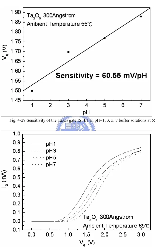
solutions at 55℃………. 54 Figure 4-29 Sensitivity of the Ta2O5 gate ISFET in pH=1, 3, 5, 7 buffer solutions
at 55℃………. 55 Figure 4-30 ID-VG curves of the Ta2O5 gate ISFET in pH=1, 3, 5, 7 buffer
solutions at 65℃………. 55 Figure 4-31 Sensitivity of the Ta2O5 gate ISFET in pH=1, 3, 5, 7 buffer solutions
at 65℃………. 56 Figure 4-32 ID-VG curves of the Ta2O5 gate ISFET in pH=1, 3, 5, 7 buffer
solutions at 75℃………. 56 Figure 4-33 Sensitivity of the Ta2O5 gate ISFET in pH=1, 3, 5, 7 buffer solutions
at 75℃………. 57 Figure 4-34 ID-VG curves of the Ta2O5 gate ISFET in pH=1, 3, 5, 7 buffer
solutions at 85℃………. 57 Figure 4-35 Sensitivity of the Ta2O5 gate ISFET in pH=1, 3, 5, 7 buffer solutions
at 85℃………. 58 Figure 4-36 Temperature sensitivity and correlation coefficient dependency of the
Ta2O5 gate ISFET………... 58 Figure 4-37 Normalize the temperature sensitivity curve of the Ta2O5 gate ISFET.. 59 Figure 4-38 ID-VG curves of the Ta2O5 gate ISFET in pH=1 buffer solution at
temperatures of 25℃, 35℃, 45℃, 55℃, 65℃, 75℃, and 85℃……… 59 Figure 4-39 ID-VG curves of the Ta2O5 gate ISFET in pH=3 buffer solution at
Figure 4-40 ID-VG curves of the Ta2O5 gate ISFET in pH=5 buffer solution at temperatures of 25℃, 35℃, 45℃, 55℃, 65℃, 75℃, and 85℃……… 60 Figure 4-41 ID-VG curves of the Ta2O5 gate ISFET in pH=7 buffer solution at
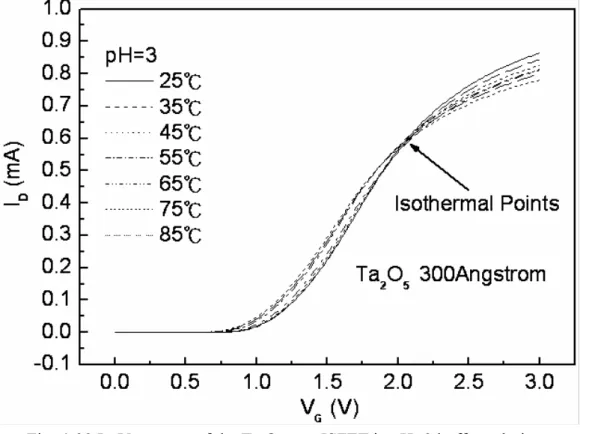
temperatures of 25℃, 35℃, 45℃, 55℃, 65℃, 75℃, and 85℃……… 61 Figure 4-42 Iso-thermal point range of the Ta2O5 gate ISFET in pH=1, 3, 5, 7
buffer solutions………..…. 61 Figure 4-43 ID-VG curves of the Thermal Oxide gate ISFET in pH=1, 3, 5, 7 buffer
solutions at 25℃………. 62 Figure 4-44 Sensitivity of the Thermal Oxide gate ISFET in pH=1, 3, 5, 7 buffer
solutions at 25℃………. 62 Figure 4-45 ID-VG curves of the Thermal Oxide gate ISFET in pH=1, 3, 5, 7 buffer
solutions at 35℃………. 63 Figure 4-46 Sensitivity of the Thermal Oxide gate ISFET in pH=1, 3, 5, 7 buffer
solutions at 35℃………. 63 Figure 4-47 ID-VG curves of the Thermal Oxide gate ISFET in pH=1, 3, 5, 7 buffer
solutions at 45℃………...………..………… 64 Figure 4-48 Sensitivity of the Thermal Oxide gate ISFET in pH=1, 3, 5, 7 buffer
solutions at 45℃………. 64 Figure 4-49 ID-VG curves of the Thermal Oxide gate ISFET in pH=1, 3, 5, 7 buffer
solutions at 55℃……….……… 65 Figure 4-50 Sensitivity of the Thermal Oxide gate ISFET in pH=1, 3, 5, 7 buffer
solutions at 55℃………. 65 Figure 4-51 ID-VG curves of the Thermal Oxide gate ISFET in pH=1, 3, 5, 7 buffer
solutions at 65℃……….……… 66 Figure 4-52 Sensitivity of the Thermal Oxide gate ISFET in pH=1, 3, 5, 7 buffer
solutions at 65℃………. 66 Figure 4-53 ID-VG curves of the Thermal Oxide gate ISFET in pH=1, 3, 5, 7 buffer
solutions at 75℃……….……… 67 Figure 4-54 Sensitivity of the Thermal Oxide gate ISFET in pH=1, 3, 5, 7 buffer
solutions at 75℃………. 67 Figure 4-55 ID-VG curves of the Thermal Oxide gate ISFET in pH=1, 3, 5, 7 buffer
solutions at 85℃……….……… 68 Figure 4-56 Sensitivity of the Thermal Oxide gate ISFET at pH=1, 3, 5, 7 buffer
solutions at 85℃………. 68 Figure 4-57 Temperature sensitivity and correlation coefficient dependency of the
Thermal Oxide gate ISFET…..………... 69 Figure 4-58 Normalize the temperature sensitivity curve of the Thermal Oxide
gate ISFET……….. 69 Figure 4-59 ID-VG curves of the Thermal Oxide gate ISFET in pH=1 buffer
solution at temperatures of 25℃, 35℃, 45℃, 55℃, 65℃, 75℃, and 85℃………. 70 Figure 4-60 ID-VG curves of the Thermal Oxide gate ISFET in pH=3 buffer
solution at temperatures of 25℃, 35℃, 45℃, 55℃, 65℃, 75℃, and 85℃………. 70 Figure 4-61 ID-VG curves of the Thermal Oxide gate ISFET in pH=5 buffer
solution at temperatures of 25℃, 35℃, 45℃, 55℃, 65℃, 75℃, and 85℃………. 71
Figure 4-62 ID-VG curves of the Thermal Oxide gate ISFET in pH=7 buffer solution at temperatures of 25℃, 35℃, 45℃, 55℃, 65℃, 75℃, and 85℃………. 71 Figure 4-63 Iso-thermal point range of the Thermal Oxide gate ISFET in pH=1, 3,
5, 7 buffer solutions……… 72 Figure 4-64 ID-VG curves of the PE Oxide gate ISFET in pH=1, 3, 5, 7 buffer
solutions at 25℃………. 72 Figure 4-65 Sensitivity of the PE Oxide gate ISFET in pH=1, 3, 5, 7 buffer
solutions at 25℃………. 73 Figure 4-66 ID-VG curves of the PE Oxide gate ISFET in pH=1, 3, 5, 7 buffer
solutions at 35℃………. 73 Figure 4-67 Sensitivity of the PE Oxide gate ISFET in pH=1, 3, 5, 7 buffer
solutions at 35℃………. 74 Figure 4-68 ID-VG curves of the PE Oxide gate ISFET in pH=1, 3, 5, 7 buffer
solutions at 45℃………. 74 Figure 4-69 Sensitivity of the PE Oxide gate ISFET in pH=1, 3, 5, 7 buffer
solutions at 45℃………. 75 Figure 4-70 ID-VG curves of the PE Oxide gate ISFET in pH=1, 3, 5, 7 buffer
solutions at 55℃………. 75 Figure 4-71 Sensitivity of the PE Oxide gate ISFET in pH=1, 3, 5, 7 buffer
solutions at 55℃………. 76 Figure 4-72 ID-VG curves of the PE Oxide gate ISFET in pH=1, 3, 5, 7 buffer
solutions at 65℃………. 76 Figure 4-73 Sensitivity of the PE Oxide gate ISFET in pH=1, 3, 5, 7 buffer
solutions at 65℃………. 77 Figure 4-74 ID-VG curves of the PE Oxide gate ISFET in pH=1, 3, 5, 7 buffer
solutions at 75℃………. 77 Figure 4-75 Sensitivity of the PE Oxide gate ISFET in pH=1, 3, 5, 7 buffer
solutions at 75℃………. 78 Figure 4-76 ID-VG curves of the PE Oxide gate ISFET in pH=1, 3, 5, 7 buffer
solutions at 85℃………. 78 Figure 4-77 Sensitivity of the PE Oxide gate ISFET in pH=1, 3, 5, 7 buffer
solutions at 85℃………. 79 Figure 4-78 Temperature sensitivity and correlation coefficient dependency of the
PE Oxide gate ISFET…..………... 79 Figure 4-79 Normalize the temperature sensitivity curve of the PE Oxide gate
ISFET……….. 80 Figure 4-80 ID-VG curves of the PE Oxide gate ISFET in pH=1 buffer solution at
temperatures of 25℃, 35℃, 45℃, 55℃, 65℃, 75℃, and 85℃……… 80 Figure 4-81 ID-VG curves of the PE Oxide gate ISFET in pH=3 buffer solution at
temperatures of 25℃, 35℃, 45℃, 55℃, 65℃, 75℃, and 85℃……… 81 Figure 4-82 ID-VG curves of the PE Oxide gate ISFET in pH=5 buffer solution at
temperatures of 25℃, 35℃, 45℃, 55℃, 65℃, 75℃, and 85℃……… 81 Figure 4-83 ID-VG curves of the PE Oxide gate ISFET in pH=7 buffer solution at
temperatures of 25℃, 35℃, 45℃, 55℃, 65℃, 75℃, and 85℃……… 82 Figure 4-84 Iso-thermal point range of the PE Oxide gate ISFET in pH=1, 3, 5, 7
Figure 4-85 The drift of ZrO2 gate ISFET with time……….. 83 Figure 4-86 The relation of ZrO2 drift voltages and gate stress voltage……… 83 Figure 4-87 The drift of Ta2O5 gate ISFET with time……… 84 Figure 4-88 The relation of Ta2O5 drift voltages and gate stress voltage…………... 84 Figure 4-89 The drift of Thermal Oxide gate ISFET with time………. 85 Figure 4-90 The relation of Thermal Oxide drift voltages and gate stress voltage… 85 Figure 4-91 The drift of PE Oxide gate ISFET with time……….. 86 Figure 4-92 The relation of PE Oxide drift voltages and gate stress voltage………. 86 Figure 4-93 VG vs Cycle time test of the ZrO2 gate ISFET in pH=7 buffer solution
at either 25℃ or 85℃……….…… 87 Figure 4-94 △VG vs Cycle time test of the ZrO2 gate ISFET in pH=7 buffer
solution at either 25℃ or 85℃………...……...……….…… 87 Figure 4-95 VG vs Cycle time test of the Ta2O5 gate ISFET in pH=7 buffer
solution at either 25℃ or 85℃………….……….. 88 Figure 4-96 △VG vs Cycle time test of the Ta2O5 gate ISFET in pH=7 buffer
solution at either 25℃ or 85℃………...……...……….…… 88 Figure 4-97 VG vs Cycle time test of the Thermal Oxide gate ISFET in pH=7
buffer solution at either 25℃ or 85℃………….……….... 89 Figure 4-98 △VG vs Cycle time test of the Thermal Oxide gate ISFET in pH=7
buffer solution at either 25℃ or 85℃………...……...…………... 89 Figure 4-99 VG vs Cycle time test of the PE Oxide gate ISFET in pH=7 buffer
solution at either 25℃ or 85℃………….………... 90 Figure 4-100 △VG vs Cycle time test of the PE Oxide gate ISFET in pH=7 buffer
Chapter 1
Introduction
1.1 Motivation of this work
The most often mentioned advantages of ISFET are very fast response, high sensitivity, batch processing capability, micro size and the potential for on-chip circuit integration. Ion-sensitive field effect transistors (ISFETs) exist some instable characteristics, such as ambient temperature changed and temperature hysteresis influence and time drift versus gate voltage stress modulation influence. In this work, we choose ZrO2, Ta2O5, Thermal Oxide, and PE Oxide as sensing films and study the sensing characteristic and figure out the feasibility of CMOS process fabrication.
In this work, some theoretical analysis of the ISFETs characteristics is studied. It is mainly based on a site-binding model and MOSFET theory. According the experiment result that can easily find proper explanations for optimum reliability characteristics for ISFETs.
1.2 Introduction the ISFET
The ISFET was that published by P. Bergveld in 1970 [1]. It have developed into a new type of chemical sensing electrode. The main part of an ISFET is the ordinary metal oxide silicon field effect transistor (MOSFET) with the gate electrode replaced by chemically sensing layers, and the sensing layers are exposed to the solution directly. The fundamental principles of ISFET will be developed from these MOSFET theories. Many theoretical and experimental studies have been published describing the behavior of this chemical sensing electronic device [2].
At first, Bergveld and Sibbald as an expression for the drain current in the linear region. Therefore changes in the drain current are attributed to changes in the electrostatic only.
Afterwards, Yates et al. [3] introduced the site-binding model in colloid chemistry to describe the properties of an oxide-aqueous electrolyte interface. This model was later adapted to describe the insulator-electrolyte interface of an ISFET. Compare with conventional pH-meter using glass electrode, the ISFET’s advantage as below: (1) High input impedance and low output impedance result and high SNR. (2) Bio-sensor or other micro-sensors can be applied. (3).Easy to achieve mass production and low cost and MOSFET process compatible. (4)Only need little media exposed and can be miniaturization.
1.3 Introduction the pH
The measurement of pH is the most widely employed test for (bio-)chemical lab. Since the first use of glass electrode to detect pH, the technology and methods have broaden the scope of pH detection. Why is the pH important to us? Because the pH is one of the most common laboratory measurements because so many chemical and biological process are dependent on pH. The detail reason describe as below:
(1) Measuring pH is essential in finding the chemical characteristics of a substance. Both the solubility of many chemicals or biomolecules in solution and the speed or rate of (bio-)chemical reactions are dependent on pH. In order to optimize the desired reaction and to prevent unwanted reactions, controlling the pH of solutions is very important.
(2) The body fluid of living organisms usually has specific pH range. The pH values of lakes, rivers, and oceans differ and depend on the kinds of animals and plants living there. The wastewater from factories and households may cause the pH changes of water and brings the environmental impact on the local or even remote inhabitants.
(3) As pH measurement is essential for control of chemical reactions, it is carried out in nearly all industries that deal with water: from the drinking water, the food and the drugs to the paper, plastics, semiconductors, cements, glass or textiles.
1.4 The pH Detect Technique
In tradition, the measuring methods for pH values fall roughly into four categories: indictor reagents, pH test strips, metal electrode methods and glass electrode methods. The glass electrode is most widely used for pH measurement due to ideal Nernstian response independent of redox interferences, short balancing time of electrical potential, high reproducibility and long lifetime. However, glass electrode has several drawbacks for many industrial applications. Firstly, they are unstable in alkaline or HF solutions or at temperatures higher 100℃. Also, they exhibit a sluggish response and are difficult to miniaturize. Moreover, they cannot be used in food or in in vivo applications due to their brittle nature. There is an increasing need to for alternative pH electrodes.
The new techniques for pH detection which include: (1) Optical-fiber-based pH sensors. (2) Mass-sensitive pH sensor. (3) Metal oxide pH sensors. (4) Conducting polymer pH sensors. (5) Nano-constructed cantilever-based pH sensors. (6) ISFET-based pH sensors. (7) pH-image sensor.
The problems in practical applications about reliability of ISFETs are continuing to be investigated in this study.
Chapter 2
Theories for the Investigation of ISFET’s Temperature and Drift
Characteristics
2.1 Basic Principles of ISFET
An anisotropic ion accumulation exists at the contact interface between an electrochemically active surface and a liquid electrolyte (Figure 2-1). Due to their different size and charge, the ions from a well-confined electric double layer close to the surface and outer charges exists between the Helmholtz planes and the neutral bulk of the solution.
Since the first report of the ISFET by Bergveld, research on new material and fabrication process to improve the sensitivity and stability has been continuously proposed [4-6]. At the same time, the mechanism of the pH response of pH ISFET has also been studied extensively [5-10].The followings are the theoretical foundations which are mostly adopted to characterize the ISFET.
2.1.1 From MOSFET to ISFET
The operation of an ISFET can best be described by comparing it with its purely electronic analogue. Figure 2-2 illustrates the similarities and differences between these two devices: The metal gate of the MOSFET of Figure 2-2(a) is replaced by the metal of a reference bare gate insulator ISFET in Figure 2-2(b). Mounting of the chips is of course different: a MOSFET can be completely encapsulated, whereas for an ISFET source and drain leads as well as chip edges have to be encapsulated carefully, meanwhile leaving the
gate area open for the contact with liquid.
For both devices the following equation is valid for the non-saturated region:
(
GS T)
DS DS OX D V V V V L W C I ⎭ ⎬ ⎫ ⎩ ⎨ ⎧ − − = 2 1 μ (2-1)with COX is the oxide capacitance per unit area, μ the electron mobility in the channel , W and
L the width and the length of the channel.
In addition, the fabrication process for MOSFET devices are so well under control that VT is also a constant, which manifests itself only as a certain threshold voltage, hence its
name, it was initially debated whether the observed ion sensitivity should be described as an additional input variable in terms of a modification of Vgs or a modification of VT. Therefore,
the second important MOSFET equation is that of the threshold voltage:
F OX B SS OX Si M T φ C Q Q Q q V =Φ −Φ − + + +2 (2-2)
where the first term reflects the difference in work function between the gate meta (ΦM) and
silicon (Φsi), the second term is due to accumulated charge in the oxide (QOX), at the
oxide-silicon interface (QSS) and the depletion charge in the silicon(QB), whereas the last term
determines the onset of inversion depending on the doping level of the silicon. All terms are purely physical in nature.
In case of the ISFET, the same fabrication process is used, resulting in the same constant physical part of the threshold voltage (Eq. (2-2)). However, in addition to this, two more contributions manifest themselves: the constant potential of the reference electrode, Eref , and
the interfacial potential Eref + χsol at the solution/oxide interface of which Ψ is the chemical
input parameter, shown to be a function of the solution pH and χsol is the surface dipole potential of the solvent and thus having a constant value. The term Ψ0 representing the
surface potential at the oxide-electrolyte interface is the key element that makes ISFET pH-sensitive.
F OX B SS OX Si sol ref T φ C Q Q Q q Ψ χ E V = + − 0−Φ − + + +2 (2-3)
2.1.2 The Oxide-Electrolyte Interface of pH Response
The surface of any metal oxide always contains hydroxyl groups, in the case of silicon dioxide SiOH groups. These group may donate or accept a proton from solution, leaving a negatively charged or a positively charged surface group respectively. In the case of silicon dioxide SiOH groups. It is indicated that equilibrium reactions can occur between protons in the solution and the hydroxyl at the SiO2 solution interface. The oxide surface charge can be described by the site-binding model, as schematically represented by Figure 2-3 which describes the equilibrium between the so-called amphoteric SiOH surface sited and the H+ -ions in the solution. These reactions can be expressed by
+ ++ ←⎯→ 2 1 SiOH SiOH H K S (2-4) + + ⎯→ ←K SiO- HS SiOH 2 (2-5)
where H represents the protons at the surface of the oxide. S+
The generally expression for the pH sensitivity of an ISFET, this response is given by: α q kT . δpH δΨ B 3 2 0 =− with (2-6) 1 3 2 1 int 2 + = β q kTC . α dif (2-7)
the parameter α is a dimensionless sensitivity parameter what varies between 0 and 1, depending on the intrinsic buffer capacity βint, of the oxide surface and the differential double-layer capacitance Cdiff. If α=1, the theoretical maximum sensitivity of -59.2mV/pH at room temperature can be obtained.
2.2 Introduction the Temperature Phenomenon
Because an ISFET is a chemical sensor based on MOSFET, ISFET’s temperature characteristics are similar to a conventional MOSFET. According to the equation of the linear region in MOSFET, we concluded that only the mobility and the threshold voltage are temperature dependent. These two factors have a negative T.C. It implies which a zero T.C. point exits in the ID-VG characteristics. We concluded a series of experiments on the temperature characteristics in different solutions, the operation currents of the zero T.C. are changed in different solutions. This results indicate that the operation conditions for zero T.C. will change along with the change in solutions.
On the operating conditions for a zero T.C., a differential configuration was used to investigate the membrane/electrolyte interface temperature coefficient. The differential configuration used dual FET’s structures, one FET was a MOSFET, the other was an ISFET. A typical example of the linear region of the dual FET’s structures in different temperatures is shown in Figure 2-4. This figure indicates that the operation currents for the MOSFET and the ISFET at different currents will yield a different T.C. Although the two FET’s have the same tendency, the T.C. of the membrane/electrolyte interface can be estimated from the following equation:
T.C.(ISFET) — T.C.(MOSFET)= T.C.(membrane/ electrolyte interface) (2-8)
Operated in the nonsaturation region in different temperatures of IDS-VGS curves for the
MOSFET were obtained. Part of the ID-VG curves are shown in Figure 2-5. A deviation in the IDS-VGS characteristics occurred as the temperature changed and it is easily to see the
isothermal point clearly. In our previous study, an ISFET with different sensing film was developed based on the MOSFET theory. Operated in the nonsaturation region in pH = 2, 4, 6, 7, 8, 10 and 12 in temperatures from 5 to 65℃ with a step of 10℃, a family of IDS-VGS
deviation in the IDS-VGS characteristics occurred as the temperature changed and it is easily to see the isothermal point clearly too. The ID-VG curve at a specific pH declined with an increase in temperature. Accordingly, and isothermal point, near zero temperature coefficient, it is indicates that a well-chosen operating point can eliminate the temperature influence in nonsaturation region because the threshold voltage is approach constant. In this study, the temperature effects on several sensing film ISFET characteristics operated in the nonsaturation and saturation regions were investigated. The threshold voltage( VT ) and drain-source current( IDS ) versus temperature characteristics will be discussed [11-12].
2.3 Introduction the Drift Phenomenon
Threshold voltage instability, commonly known as drift, has seriously limited the commercial viability of ISFET-based sensors by imposing special requirements for burn-in, packaging or compensation. Drift is typically characterized by a relatively slow, monotonic, temporal change in the threshold voltage of the ISFET, which is not caused by variations in the electrolyte composition. General explanations proposed for drift phenomenon include electric field enhanced ion migration within the gate insulator as well as electrochemical non-equilibrium conditions at the insulator -solution interface, injection of electrons from the electrolyte at strong anodic polarizations, creating negative space charge inside the insulator films, and slow surface effect. The drift is thought to be caused by the slow conversion of the surface to a hydrated during contact with the solution. The following models, which are classified according to the location where the mechanism of pH-sensitivity is presumed to occur, will help us to have a further understanding of the transport of mobile ions.
2.3.1 Physical Model for Drift
The model presented in this work quantitatively explains drift in terms of hydration [13-16]. In particular, the time dependence of drift is derived by considering the correlation between the rate of hydration and the hopping and /or trap-limited transport of water-related species. The gate voltage drift in pH ISFET’s is a relatively slow process which occurs over a period of several hours, it is reasonable to hypothesize that this phenomenon is associated with transport in the insulator. In particular, the motion within this gate insulator is expected to be characterized by relatively long transit time.
It is well known that the surface is slowly converted to a hydrated sensing layer as result of exposure to an aqueous electrolyte. The chemical modification of the insulator surface implies that the dielectric constant of the hydration layer will differ from that of the insulator bulk. Therefore, the overall insulator capacitance, which is determined by the series combination of the capacitance of the hydration layer, it will exhibit a relatively slow, temporal change as hydration proceeds. The rate of hydration which has recently been accurately modeled by a hopping transport mechanism, known as dispersive transport. In amorphous solid, dispersive transport arising from a hopping motion via localized states, result in a characteristic power-law time decay of diffusivity given by:
1 0 00( ) ) (t =D ω t β− D (2-9)
where D00 is a temperature-dependent diffusion coefficient which obeys an Arrhenius relationship, ω0 is the hopping attempt frequency, and β is the dispersion parameter satisfying 0<β<1. Physically, the time-dependent transport properties result from the dispersion in the separation distances between nearest-neighbor localized sites and/or the dispersion in trap energy levels. Dispersive transport leads to a decay in the density of sites/traps occupied by the species undergoing transport. This decay is described by the stretched-exponential time
dependence given by ] ) / exp[( ) 0 ( ) ( / / t N t τ β NS T =Δ S T − Δ (2-10)
where ΔNS/T(t) is the area density (units of cm-2) of sites/traps occupied, τ is the time constant
associated with structural relaxation, and β is the dispersion parameter characterizing dispersive transport.
2.3.2 Drift Expression
One means of operating an ISFET is in the feedback mode, where a constant drain current is maintained by applying a compensating feedback voltage to the solution side of the gate voltage ( e.g., a reference electrode). Therefore, the temporal change is the overall insulator capacitance resulting from hydration leads to a drift in compensating feedback voltage. In other words, when drift phenomenon occurs at the surface of an actively-biased ISFET, the gate voltage will simultaneously exhibit a change to keep a constant drain current. The change in the gate voltage can be written as
) 0 ( ) ( ) ( G G G t V t V V = − Δ (2-11)
Since the voltage drop inside of the semiconductor is kept constant in the feedback mode, ΔVG(t) becomes )] 0 ( ) ( [ )] 0 ( ) ( [ ) ( FB FB ins ins G t V t V V t V V = − + − Δ (2-12)
where VFB and Vins represent the flatband voltage and the voltage drop across the insulator,
respectively. The flatband voltage is given by
OX SS OX Si sol ref FB C Q Q q Ψ E V = +χ − 0 −Φ − + (2-13) The voltage drop across the insulator, Vins, is given by
OX inv B ins C Q Q V = −( + ) (2-14)
solution are held constant, the variations in Eref, χsol, Ψ0, and ΦSi can be neglected, so the drift can be rewritten as ⎥ ⎦ ⎤ ⎢ ⎣ ⎡ − + + + − = Δ ) 0 ( 1 ) ( 1 ) ( ) ( I i inv B SS OX G C t C Q Q Q Q t V (2-15)
The gate oxide of the fabricated ISFET was composed of two layers in this study, a lower layer of thermally-grown SiO2 of thickness, xL, and an upper layer of PECVD SiO2 of
thickness, xU.. CI(0) is the effective insulator capacitance given by the series combination of
the thermally-grown SiO2 capacitance, εL/xL, and the PECVD SiO2 capacitance, εU/xU. Ci(t) is
analogous to CI(0), but an additional hydrated layer of capacitance, εHL/xHL, at the
oxide-electrolyte interface must be took into consideration, and the PECVD SiO2 capacitance is now given by εU/[xU-xHL]. The series combinations of the capacitances are illustrated in
Figure 2-7. The simplified expression for drift is, therefore, given by [17] ) ( ) ( ) (t Q Q Q Q x t V HL HL U HL U inv B SS OX G ⎟⎟ ⎠ ⎞ ⎜⎜ ⎝ ⎛ − + + + − = Δ ε ε ε ε (2-16)
As is evident from From this equation (2-16), drift is directly proportional to the thickness of the modified surface layer. Therefore, the time dependence of drift is identical to that associated with the growth of this layer. By considering the time dependence of the diffusion coefficient associated with dispersive transport, an expression for xHL(t) is given by
[
]
{
1 exp ( /τ)β}
) ( ) (t x t xHL = HL ∞ − − (2-17) where xHL(∞) is given by hydr D T S HL N A N D x β ωβ (0) ) (∞ = 00 0 1Δ / − (2-18)where AD represents the cross-sectional area, and Nhydr is the average density of the hydrating
species per unit volume of hydration layer. The overall expression for the gate voltage drift is given by
[
]
{
τ β}
ε ε ε ε ) / ( exp 1 ) ( ) ( ) (t Q Q Q Q x t V HL HL U HL U inv B SS OX G ⎟⎟ ∞ − − ⎠ ⎞ ⎜⎜ ⎝ ⎛ − + + + − = Δ (2-19)We can expect that if the time of gate oxide immersing in the test-solution is long enough (determined by the constant τ ), the gate voltage drift will approach a constant value which is greatly dependent on the hydration depth, xHL(∞).
Chapter 3
Procedures of the Experiment
To investigate the properties of membrane as the pH-sensing layers, the ISFET were fabricated. All processes were done in NDL (National Nano Device Laboratory)
and Nano Facility center. The schematic diagrams of ISFET is presented and corresponding graph is shown in Figure 3-1.
3.1 ISFET Fabrication Process Flow
(a) RCA clean
Wet-oxidation, 6000Å, temperature = 1050°C for 65 minutes (b) Defining of Source/Drain (mask 1)
BOE wet-etching of SiO2
(c) Screening dry oxidation thickness=300Å, temperature=1050°C for 12 minutes Source/Drain ion implantation
Source/Drain annealing, 950°C, 60 minutes (d) PECVD SiO2 for passiveness, 1μm
(e) To define contact hole and gate region (mask 2) BOE wet-etching of SiO2
(f) Dry oxide thickness=100Å, temperature=850°C for 60 minutes (g) Sensing layer 1, 300Å
Defining of sensing region (mask 3) HF wet-etching of SiO2
(i) Al evaporation, 5000Å (mask 5)
3.2 Experiment details
3.2.1 Gate Region Formation
RCA clean is usually performed at wafer starting to reduce the effect of diffusion ions, particles and native oxide. RCA clean will ensure the integrity of device electricity. In order to create a Source/Drain region, the next step 600Å thickness wet oxide is deposited as blocking layer for Source/Drain implant. The density and the energy of Source/Drain implant is 5E15 (1/cm2) and 25Kev with phosphorus dopant, respectively. In our experiment, p-type wafer is used. After Source/Drain implanting following a 950°C 30minutes N+ anneal performed to activate the dopants.
We do not need to deposit PE-oxide with thickness 1um in standard MOSFET, but it is necessary to do which protect the structure of a pH-ISFET, when the ISFET’s will operating in a long period, during this period, we need to avoid ion’s diffusion in the structure and affect the electrical characteristics [18]. In order to avoid this influence, a thick PE-oxide deposition can eliminate this effect. After PE-oxide depositing, 100Å thickness dry oxide was grown as gate oxide.
3.2.2 Sensing Layer Deposition
Methods of deposited sensing membrane as gate material are different which is the most important part in our experiment. The drift, hysteresis and sensitivity will improve by different layers [19]. For comparing these sensing layers, several deposition techniques were performed. Low- pressure nitride (LP- nitride) and PE-oxide are deposited as sensing
layers. We adopted LPCVD to obtain low stress nitride and high sensitivity, so it is good sensing layer. There are so many researches on it [20]. However, PE-oxide drift and sensitivity are unstable in different electrolytes. In CMOS process, tungsten and tantalum are popularly used. By using different barriers, drift lowing for a long period of tome and compatible with CMOS can be accomplished.
3.3 Measurement System
3.3.1 Preparation Before Measuring
To define the characteristics of the device, we use HP4156A to measure the I-V curve of ISFET. The measurement system is showed in Figure 3-2. Otherwise, light will produce serious influence on the ISFET, so that we measurement in the dark box to prevent light influence.
After device being made, we glue a container on the wafer. Entire sensing layer region must be included in the opening under the container. The material of the container is made by silica gel and the bottom has to be small enough to avoid touching other devices. However, the opening on the top has to be big enough for insert reference electrode.
The pH-solution that we use is made from Riedel-deHzen and pH-value is 1, 3, 5, 7 buffer solutions. The electric potential of the pH-solution is always floating. The disturbance from the environment would induce the electric potential variance of the solution. By eliminating this variance, a reference electrode is needed to put into the pH-solution.
3.3.2 Measurement Set-Up
In the beginning of the measurement, the reference electrode is suspended on the air over the container. The pH-solution is filled in the container. It is noticed that the pH-solution must touch the sensing layer entirely because of the small opening.
In the setup of HP-4156A semiconductor parameter analyzer system, substrate is grounded and the reference electrode is sweeping to different voltage. In the measurement of sensitivity, the response of the pH-ISFET is the function of time and at the first, we check the ID-VD curve to make sure the ISFET device is work as a MOSFET. On the other hand, we also should decide the drain bias from ID-VD to ensure the both IFET are operating in linear region while ID-VG measurement.
The ISFET held at VG= 1V, 2V, 3V, 4V, and 5V. The typical set of ID-VD curves for the ZrO2, Ta2O5, Thermal Oxide, and PE Oxide gate ISFET are shown in Figure 3-3, Figure 3-4, Figure 3-5, Figure 3-6.
The pH-solution in the container is about several milliliters. In order to control the accuracy of the result, the container has to be washed by the next pH-solution after measuring previous pH-solution.
3.3.3 Temperature Measurement Set-Up
For characterizing the temperature influence of ISFETs, we measured I-V curves for etch film with changing the pH-solution in order of pH 1, 3, 5, 7 buffer solutions and controlling the different ambient temperature about 25°C, 35°C, 45°C, 55°C, 65°C, 75°C, and 85°C. For each temperature value, we wait the 15 minutes then measured the ID-VG curves which the pH-ISFET had been covered by the pH-solution. The measurement system is showed in Figure 3-7. Figure 3-8 illustrates the detection principle of pH. Firstly, we obtain
the pH1 transconductance, it is purpose to get maximum gain. The second step we decide the pH1’s VG then decide the IDS. At last, we can obtain the pH3, pH5, pH7’s VG. When we
change the different pH buffer solution, we must use the pH7 buffer solution first, then pH5, pH3, and pH1, it is purpose to get better performance which let the pH buffer solution concentration from low to high.
Chapter 4
Results and Discussions
4.1 Temperature Sensitivities of Various Membranes
4.1.1 ZrO2 membrane gate ISFET
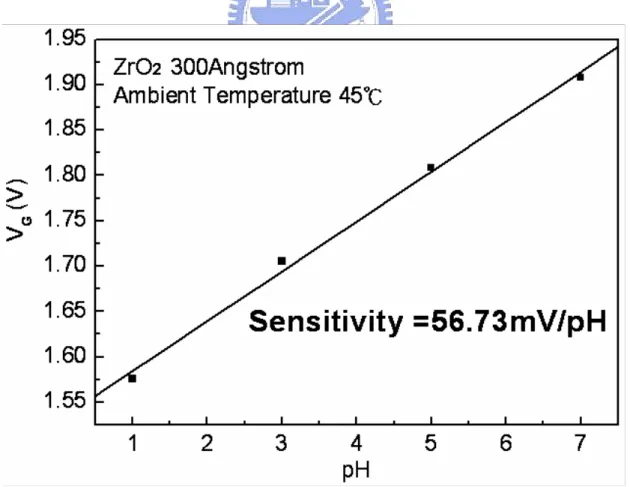
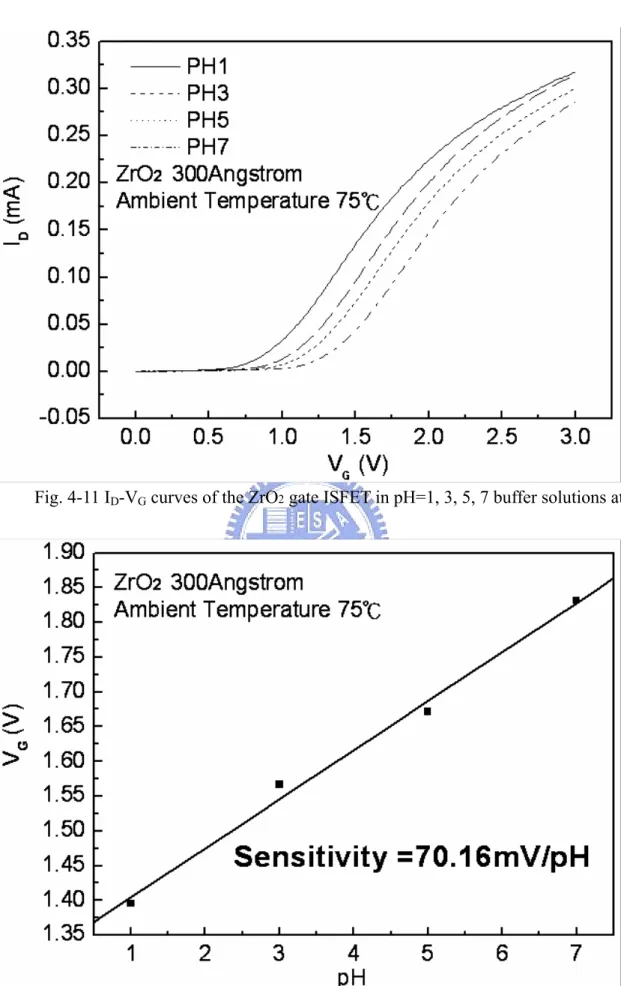
Figure 4-1~4-14 are the ID-VG curves and sensitivities of ZrO2 gate ISFET in pH=1, 3, 5, 7 buffer solutions at 25℃, 35℃, 45℃, 55℃, 65℃, 75℃, and 85℃. The measuring data are sorted in table 4-1. Figure 4-15 is temperature sensitivity correlation coefficient. The measuring data are sorted in table 4-3. Figure 4-16 is normalize the temperature sensitivities curve. The measuring data are sorted in table 4-2. According to the data about table 4-3, we can find that ZrO2 gat ISFET temperature sensitivity is increase progressively.
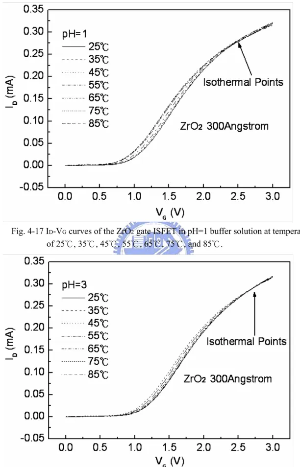
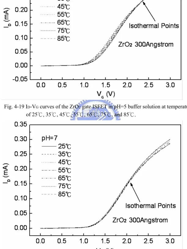
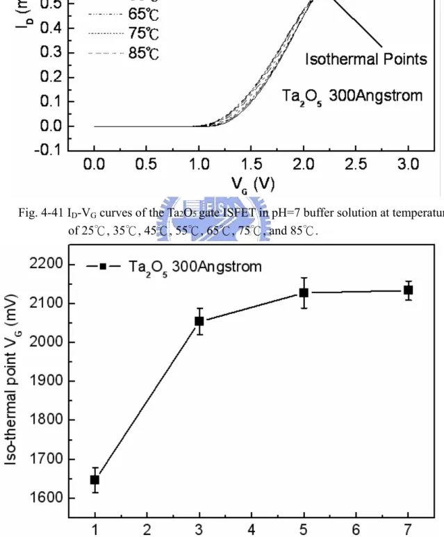
Figure 4-17~4-20 the ID-VG curve at a specific pH declined with an increase in temperature. That can fine the isothermal point as show as Figure 4-21, it is near zero temperature coefficient, this indicates that a well-closen operating point can eliminate the temperature influence, the measuring data are sorted in table 4-4.
4.1.2 Ta2O5 membrane gate ISFET
Figure 4-22~4-35 are sensitivities of Ta2O5 gate ISFET in pH=1, 3, 5, 7 buffer solutions at 25℃, 35℃, 45℃, 55℃, 65℃, 75℃, and 85℃. The measuring data are sorted in table 4-1. Figure 4-36 is temperature sensitivity correlation coefficient. The measuring data are sorted in table 4-3. Figure 4-37 is normalize the temperature sensitivities curve. The measuring data are sorted in table 4-2. According to the data about table 4-3, we can find that
Ta2O5 gat ISFET temperature sensitivity is decrease progressively.
Figure 4-38~4-41 the ID-VG curve at a specific pH declined with an increase in temperature. That can fine the isothermal point as show as Figure 4-42, it is near zero temperature coefficient, this indicates that a well-closen operating point can eliminate the temperature influence, the measuring data are sorted in table 4-4.
4.1.3 Thermal Oxide membrane gate ISFET
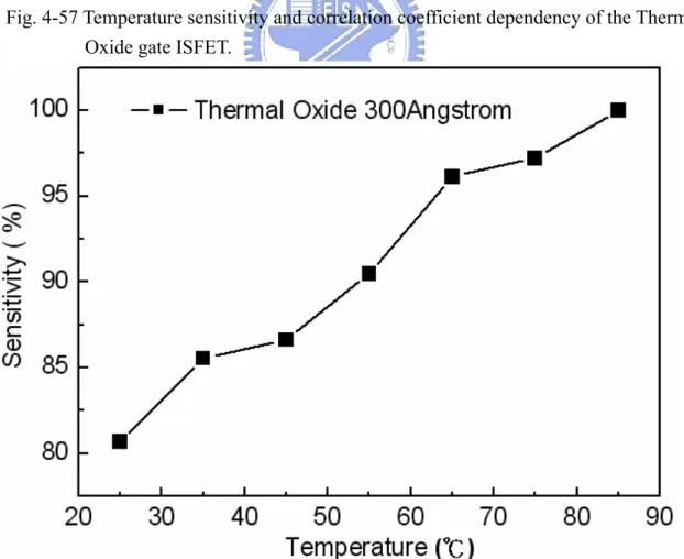
Figure 4-43~4-56 are sensitivities of Thermal Oxide gate ISFET in pH=1, 3, 5, 7 buffer solutions at 25℃, 35℃, 45℃, 55℃, 65℃, 75℃, and 85℃. The measuring data are sorted in table 4-1. Figure 4-57 is temperature sensitivity correlation coefficient. The measuring data are sorted in table 4-3. Figure 4-58 is normalize the temperature sensitivities curve. The measuring data are sorted in table 4-2. According to the data about table 4-3, we can find that Thermal Oxide gat ISFET temperature sensitivity is increase progressively.
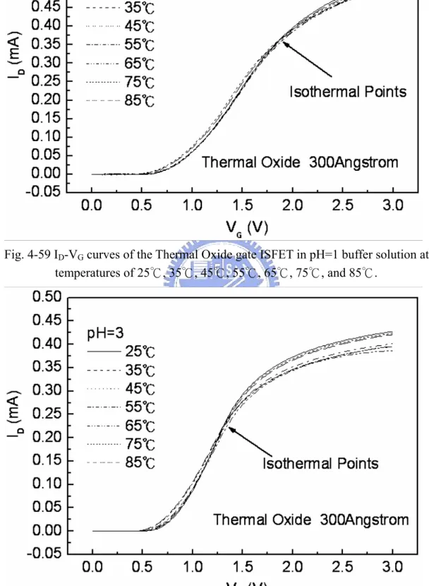
Figure 4-59~4-62 the ID-VG curve at a specific pH declined with an increase in temperature. That can fine the isothermal point as show as Figure 4-63, it is near zero temperature coefficient, this indicates that a well-closen operating point can eliminate the temperature influence, the measuring data are sorted in table 4-4.
4.1.4 PE Oxide membrane gate ISFET
Figure 4-64~4-77 are sensitivities of PE Oxide gate ISFET in pH=1, 3, 5, 7 buffer solutions at 25℃, 35℃, 45℃, 55℃, 65℃, 75℃, and 85℃. The measuring data are sorted in table 4-1. Figure 4-78 is temperature sensitivity correlation coefficient. The measuring data are sorted in table 4-3. Figure 4-79 is normalize the temperature sensitivities curve. The measuring data are sorted in table 4-2. According to the data about table 4-3, we can find that
PE Oxide gat ISFET temperature sensitivity is decrease progressively.
Figure 4-80~4-83 the ID-VG curve at a specific pH declined with an increase in temperature. That can fine the isothermal point as show as Figure 4-84, it is near zero temperature coefficient, this indicates that a well-closen operating point can eliminate the temperature influence, the measuring data are sorted in table 4-4.
4.1.5 Followings are the discussions of the measurement results:
It is very interested in sensitivity measurement result. Why, there are ZrO2 gate ISFET and Thermal Oxide gate ISFET temperature sensitivity increase progressively?
Why, there are Ta2O5 gat ISFET and PE Oxide gate ISFET temperature sensitivity decrease progressively?
According to the Eq. (2-6), the parameter α is a dimensionless sensitivity parameter and T is temperature parameter. If T is multiply α and product is increase that cause temperature sensitivity is upwardly. Otherwise, if T is multiply α and product is decrease that cause sensitivity is downward.
Accordingly, an isothermal point of the ZrO2, Ta2O5, Thermal Oxide, and PE Oxide in pH=1, 3, 5, 7 buffer solutions at 25℃, 35℃, 45℃, 55℃, 65℃, 75℃, and 85℃, the pH response increases monotonically as the temperature increases.
4.2 Drift Characteristics of Gate Stress Voltages in Various Membranes
4.2.1 ZrO2 membrane gate ISFET
Figure 4-85 shows the drift of ZrO2 gate ISFET with time. It is obviously shows a strong relation of gate drift and gate stress voltages. When the gate voltage is controlled as -0.5V, the drift voltage will decrease from -57.94 mV to -3.45mV in six hours measurement. The improvement of the drift voltage reaches 94.05%. In order to confirm that the method works, a ZrO2 film ISFET has also measured by various gate voltages. Figure 4-86 shows the relation of drift voltages and gate stress voltages, and the data are sorted in table 4-5.
4.2.2 Ta2O5 membrane gate ISFET
Figure 4-87 shows the drift of Ta2O5 gate ISFET with time. It is obviously shows a strong relation of gate drift and gate stress voltages. When the gate voltage is controlled as -0.5V, the drift voltage will decrease from 40.6mV to 25.48mV in six hours measurement. The improvement of the drift voltage reaches 37.24%. In order to confirm that the method works, a Ta2O5 film ISFET has also measured by various gate voltages. Figure 4-88 shows the relation of drift voltages and gate stress voltages, and the data are sorted in table 4-5.
4.2.3 Thermal Oxide membrane gate ISFET
Figure 4-89 shows the drift of Thermal Oxide gate ISFET with time. It is obviously shows a strong relation of gate drift and gate stress voltages. When the gate voltage is controlled as -0.5V, the drift voltage will decrease from 56.12mV to 2.94mV in six hours measurement. The improvement of the drift voltage reaches 94.76%. In order to confirm that
the method works, a Thermal Oxide film ISFET has also measured by various gate voltages. Figure 4-90 shows the relation of drift voltages and gate stress voltages, and the data are sorted in table 4-5.
4.2.4 PE Oxide membrane gate ISFET
Figure 4-91 shows the drift of PE Oxide gate ISFET with time. It is obviously shows a strong relation of gate drift and gate stress voltages. When the gate voltage is controlled as 1V, the drift voltage will decrease from 45.54mV to 0.92mV in six hours measurement. The improvement of the drift voltage reaches 97.98%. In order to confirm that the method works, a PE Oxide film ISFET has also measured by various gate voltages. Figure 4-92 shows the relation of drift voltages and gate stress voltages, and the data are sorted in table 4-5.
4.2.5 Followings are the discussions of the measurement results:
According to the table 4-5, it is a simple and cheap way to solve the drift problem is presented which described the relation of drift and gate voltage. A constant various gate voltages are biased in the sensing layer with reference electrode. The improvement of drift voltages reaches higher. This may result from the gate electric field affecting the ions to diffusive into the gate insulator. To use this method, we can change different gate voltages which get a series of drift voltage characteristic. By this way, we can find the point about gate voltage which let drift approach to 0V for each membrane gate ISFET, it is very important to us for ISFET application. Then we will be commercialize the ISFET with a very low drift rate in a simple way.
4.3 Drift Characteristics Hysteresis of Cycle Time Test in Various
Membranes
4.3.1 ZrO2 membrane gate ISFET
Figure 4-93~4-94 are drift hysteresis of ZrO2 gate ISFET in pH=7 buffer solution at either 25℃ or 85℃. The measuring data are sorted in table 4-6 and table 4-10. According to table 4-11, the percentages of accuracy after second cycle time are about 1.30% at 25℃ and 1.96% at 85℃.
4.3.2 Ta2O5 membrane gate ISFET
Figure 4-95~4-96 are drift hysteresis of Ta2O5 gat ISFET in pH=7 buffer solution at either 25℃ or 85℃. The measuring data are sorted in table 4-7 and table 4-10. According to table 4-11, the percentages of accuracy after second cycle time are about 1.60% at 25℃, and 1.69% at 85℃.
4.3.3 Thermal Oxide membrane gate ISFET
Figure 4-97~4-98 are drift hysteresis of Thermal Oxide gat ISFET in pH=7 buffer solution at either 25℃ or 85℃. The measuring data are sorted in table 4-8 and table 4-10. According to table 4-11, the percentages of accuracy after second cycle time are about 3.66% at 25℃, and 4.12% at 85℃.
4.3.4 PE Oxide membrane gate ISFET
Figure 4-99~4-100 are drift hysteresis of PE Oxide gat ISFET in pH=7 buffer solution at either 25℃ or 85℃. The measuring data are sorted in table 4-9 and table 4-10. According to table 4-11, the percentages of accuracy after second cycle time are about 3.68% at 25℃, and 4.19% at 85℃.
4.3.5 Followings are the discussions of the measurement results:
According to the Figure 4-94, Figure 4-96, Figure 4-98, Figure 4-100, we can see that cycle time 1 is toward gate voltage hysteresis larger then the other cycle time, it is initial drift characteristic of ISFET. If we want to know the ISFET gate voltage drift hysteresis at different temperatures, we must calculate hysteresis with beginning at second cycle.
Table 4-12 shows percentages of gate voltage drift hysteresis are smaller then 5% of all membranes. It is indirect identification that the confidence of this thesis experiment results are very high.
4.4 Conclusions
In this thesis of our experiment is to study and obtain the most suitable membrane which is compatible with CMOS fabrication processes to be a sensing layer for ISFET. We choose four membranes of ZrO2, Ta2O5, Thermal Oxide, and PE Oxide to be sensing films.
The first purpose is studying the temperature sensitivity characteristic. According to the Eq. (2-6), the parameter α is a dimensionless sensitivity parameter and T is temperature parameter. If T is multiply α and product is increase that cause temperature sensitivity is upwardly. Otherwise, if T is multiply α and product is decrease that cause sensitivity is
downward. There are ZrO2 gate ISFET and Thermal Oxide gate ISFET temperature sensitivity increase progressively. There are Ta2O5 gat ISFET and PE Oxide gate ISFET temperature sensitivity decrease progressively.
The second purpose is studying the temperature isothermal point of the four membranes in pH=1, 3, 5, 7 buffer solutions at 25℃, 35℃, 45℃, 55℃, 65℃, 75℃, and 85℃, the pH response increases monotonically as the temperature increases. In other words, the temperature isothermal point is temperature balance point in pH=1, 3, 5, 7 buffer solutions at 25℃, 35℃, 45℃, 55℃, 65℃, 75℃, and 85℃. We can obtain a well-chosen operating point that can eliminate the temperature influence in this region.
The third purpose is studying the gate voltage drift characteristic. According to the table 4-5, it is a simple and cheap way to solve the drift problem is presented which described the relation of drift and gate voltage. A constant various gate voltages are biased in the sensing layer with reference electrode. The improvement of drift voltages reaches higher. This may result from the gate electric field affecting the ions to diffusive into the gate insulator. To use this method, we can change different gate voltages which get a series of drift voltage characteristic. By this way, we can find the point about gate voltage which let drift approach to 0V for each membrane gate ISFET, it is very important to us for ISFET application. Then we will be commercialize the ISFET with a very low drift rate in a simple way.
The fourth purpose is studying the drift characteristics hysteresis of cycle time test in various membranes. According to the Figure 4-94, Figure 4-96, Figure 4-98, Figure 4-100, we can see that cycle time 1 is toward gate voltage hysteresis larger then the other cycle time, it is initial drift characteristic of ISFET. If we want to know the ISFET gate voltage drift hysteresis at different temperatures, we must calculate hysteresis with beginning at second cycle.
Table 4-12 shows percentages of gate voltage drift hysteresis are smaller then 5% of all membranes. It is indirect identification that the confidence of this thesis experiment results
Chapter 5
Future Work
5.1 Temperature and Gate Voltage Stress Modulation influence
In our experiments, we investigated the ISFET’s reliability with temperature and gate voltage stress modulation individual. Therefore, how to link these factors influence range about temperature and gate voltage stress modulation together, and how to control the substrate voltage to make drift voltage become zero for each membrane gate ISFET, and how to design the circuit to realize our idea.
At present, the temperature hysteresis of the gate ISFET is not investigate deeply, and how to reduce it will be study more necessary. A perfect model of gate voltage stress with drift voltage should also be built in the future.
References
[1] P. Bergveld, “Development of an ion sensitive solid-state device for neurophysiological measurements”, IEEE Trans.Biomed. Eng.,vol. BME-17, pp. 70-71, 1970.
[2] L. L. Chi, “Study on extended gate field effect transistor with tin oxide sensing membrane”, Material Chemistry and Physics 63, pp. 19-23, 2000.
[3] D. E. Yates, S. Levine and T.W. Healy, Site-binding model of the electrical double layer at the oxide/water interface, J. Chem. Soc., Faraday Trans. 70, pp. 1807-1808, 1974.
[4] T. Matsuo and M. Esashi, Methods of ISFET fabrication, Sens. Actuators 1, pp.77-96, 1981.
[5] M. Grattarola and G. Massobrio, Bioelectronics handbook: MOSFETs, biosensors, and neurons, McGraw-Hill, New York, pp. 34-68, 1998.
[6] P. Bergveld, Thirty years of ISFETOLOGY: What happened in the past 30 years and what may happen in the next 30 years, Sens. Actuators B 88, pp. 1-20. 2003.
[7] W. Olthuis, Chemical and physical FET-based sensors or variations on an equation, Sens. Actuators B 105, pp. 96-103. 2005.
[8] L. Bousse, N. F. de Rooij, and P. Bergveld, Operation of chemically sensitive field-effect sensors as a function of the insulator-electrolyte interface, IEEE Trans. Electron Devices
ED-30, pp. 1263-1270. 1983.
[9] R.E.G. van Hal, J.C.T. Eijkel and P. Bergveld, A novel description of ISFET sensitivity with the buffer capacity and double-layer capacitance as key parameters, Sens. Actuators B 24-25, pp. 201-205. 1995.
[10] R.E.G. van Hal, J.C.T. Eijkel and P. Bergveld, A general model to describe the electrostatic potential at electrolyte oxide interfaces, Adv. Coll. Interf. Sci. 69, pp. 31-32. 1996.
[11] Y. A. Tarantov and A.S. Kartashev, “Optical and thermal sensitivity of pH-ISFET with Ta2O5 membrane,” Sens. Actuators A, vol. 28, pp. 197-198, 1991.
[12] Sentron, Inc., Sentron pH system instruction manual, pp. 1-4. 2001.
[13] S. Jamasb, S.D. Collins and R. L. Smith, A physical model for threshold voltage instability in Si3N4-gate H+-sensitive FET’s (pH ISFET’s), IEEE Trans. Electron Devices 45, pp. 1239-1245. 1998.
[14] J. C. Chou, “Ion sensitive field effect transistor with amorphous tungsten trioxide gate for pH sensing”, Sensors and Actuators B 62, pp. 81-87, 2000.
[15] H. K. Liao, “Study of amorphous tin oxide thin films for ISFET applications”, Sensors and Actuators B 50, pp. 104-109, 1998.
[16] J. C. Chou, “Preparation and study on the drift and hysteresis properties of the tin oxide gate ISFET by the sol–gel method”, Sensors and Actuators B 86, pp. 58-62, 2002
[17] S. Jamasb, An analytical technique for counteracting drift in Ion-Selective Field Effect Transistors (ISFETs), IEEE Sens. J. 4, pp. 795-801, 2004.
[18] G. T. Yu, “Hydrogen ion diffusion coefficient of silicon nitride thin films”, Applied Surface Science 202, pp. 68-72, 2002.
[19] Y. Vlasov, “Investigation of pH-sensitivity ISFETs with oxide and nitride membranes using colloid chemistry method”, Sensors and Actuators B, 1 pp. 357–360, 1990.
[20] P. Hein, “Drift behavior on ISFET with nitride gate insulator”, Sensors and Actuators B, 13-14 pp. 655–656, 1993.
(a) (b)
Fig. 2-2 Schematic representation of (a) MOSFET, (b) ISFET
Fig. 2-3 Schematic representation of the site-binding model
Drain
Source
Gate
Fig. 2-4 ID-VG characteristic of MOSFET and ISFET in different temperatures.
Fig. 2-5 ID-VG characteristic of MOSFET in different temperatures. Isothermal point
Fig. 2-6 ID-VG characteristic of ISFET in different temperatures.
(a) (b)
Fig. 2-7 Series combination of the (a) initial (b) hydrated insulator capacitance
Silicon
Thermal Oxide
Sensing Layer
Solution
Hydration
(a) (b) ` (c) (d) Si substrate Wet oxide Si substrate BOE wet-etching Si substrate S/D implant Screen Oxide PE Oxide
(e) (f) (g) (h) Dry Oxide Sensing layer 1 Sensing layer 2
(i)
Fig. 3-1 Corresponding graph for fabricate process flow.
Fig. 3-2 Shows the set up of measurement with the HP4156A Semiconductor Parameter Analyzer at room temperature.
Source
Drain
Drain
Fig. 3-3 ID-VD curve of the 300Å ZrO2-gate ISFET.
Fig. 3-5 ID-VD curve of the 300Å Thermal Oxide-gate ISFET.
Fig. 3-6 ID-VD curve of the 300Å PE Oxide-gate ISFET.
Fig. 3-7 Shows the set up of measurement with the HP4156A Semiconductor Parameter Analyzer and temperature controller.
Fig. 3-8 Detection principle of different VG.
0 0.0001 0.0002 0.0003 0.0004 0.0005 0.0006 0.0007 0 0.5 1 1.5 2 2.5 3 Vg Id pH=1 pH=7
Fig. 4-1 ID-VG curves of the ZrO2 gate ISFET in pH=1, 3, 5, 7 buffer solutions at 25℃.
Fig. 4-3 ID-VG curves of the ZrO2 gate ISFET in pH=1, 3, 5, 7 buffer solutions at 35℃.