Abstract -We reported a design and fabrication by using Micro-Electro-Mechanical-Systems (MEMS) processes of a planar 64-channel Multi-Electrode-Array (MEA) chip for recording and/or stimulating cells or tissue slice. The 8 multi-channels recording system was designed to verify the bio-electronic signal detected from the MEA chip. The active electrode area can be 20 μm x 20 μm or 40 μm x 40 μm and with 200 μm or 140 μ m space between electrodes, and the metal circuit layout is protected by thin silicone dioxide. Then, the DC measurement to prove this MEA chip device can detect bio-electronic signal normally and immersing the MEA chip in the physiological saline buffer solution to verify that the performance in the AC condition.
Keywords
—
MEA chip, MEMS, Electronic propertyI. INTRODUCTION
Multi Electrodes Array (MEA) chip has been used to stimulate and/or record cellular or tissue electrical activities [1-4]. It usually applies to the neuron fiber and brain slice to study electrical activities to help the research workers to understand the complex nervous system [5, 6]. It can be used for drug screening by monitoring electrical responses to the drugs [7]. In this paper, we will demonstrate the design and fabrication of a MEA chip by using MEMS technologies. We constructed the DC and AC measurement method to verify the MEA chip electronic properties that was suitable for sensing the electronic signal form the bio. Besides, we also designed a recording system to process the sensing bio-electronic signal from the MEA chip.
II. MATERIALS AND METHODS
A. Specifications of MEA chip
There are four types MEA chip which discriminate the difference from the electrodes size and the distance between the centers of two electrodes. Four different specifications are fabricated, which include 1) type 1: 40μm x 40μm, 200μm, 2.88 mm x 2.88 mm; 2) type 2: 20μm x 20μm, 200μm, 2.56 mm x 2.56 mm;3) type 3: 40μm x 40μm, 140μm, 1.02 mm x 1.02 mm; 4) type4: 20μm x 20μm, 140μm, 1.00 mm x
1.00 mm, numbers shown are the size of electrodes, the distance between the center of two electrodes and total area, respectively. There are 8 x 8 array and total of 64 square electrodes made on the glass substrate that chip size is 24.5 mm x 24.5 mm.
B. Fabrication procedure of MEMS of MEA chip
The using of fabrication processes to accomplish the MEA chip (Fig. 1).
Fig. 1 Fabrication procedure of MEMS for MEA chip
We first used Hexamethyldisilizane (HMDS) to clean the glass substrate and thus enhance the adhesion between photoresist and glass. Then spin coating the photoresist (S1813, Shipley) on the wafer by using the spin coater, followed by exposing the sample to the I-line of Mercury lamp.
The Design and Fabrication of Two-Dimension
Multi-Electrodes Array Chip and System
Jian-Ming Chen
1, Jhen-Gang Huang
2, Chii-Wann Lin
1, 2, 31Dept of Elec Eng, National Taiwan University, Taipei, Taiwan, 106, R.O.C. 2Inst. of Biomed Eng, National Taiwan University, Taipei, Taiwan, 100, R.O.C. 3Center for Nano Science and Technology, National Taiwan University, Taipei, Taiwan, R.O.C.
0-7803-8439-3/04/$20.00©2004 IEEE 2426
Proceedings of the 26th Annual International Conference of the IEEE EMBS
San Francisco, CA, USA • September 1-5, 2004
Development was done by immersing the sample in the developing solution (MF319, Shipley) and followed by wet etching the glass substrate with BOE. Deposition of the chromium with E-beam and formed the MEA pattern. The rest of the procedures include depositing 600nm silicon dioxide with PECVD to protect the MEA metallic circuit from buffer solution. Through photolithography, wet etching, deposing 550 nm chromium and 50nm gold and then lift-off the photoresist to etch the silicon dioxide, which form the microelectrodes and then depose the metal to construct the microelectrodes array.
C. Electronic property verification of MEA chip
DC electronic property is done by measuring the impendance between microelectrode and the connecting pad surrounding the chip edge. Under the microscope, using tungsten probes (tip diameter is 1μm) in Fig. 2 configuration, we can measure the impedance from a multimeter (HP 34401A). To further test of the Au microelectrode surface, a piece of clear HMDS with a hole in it’s center was adhered to the MEA chip. With PBS solution the hole and submersed an AgCl electrode in the PBS, we then sent a small sinusoidal stimulus (50 mV in amplitude) and sweep the frequency from 100 Hz to 10 KHz. The module and phase were read from a LCR meter (LCR-821, GW) for further analysis.
Fig. 2 The AC and DC measurement configuration.
D. Bio-electronic signal recording system
The recording system (Fig. 3) included the MEA chip holder (Fig. 4), electronic circuit hardware (Fig. 5), AD converter and the recording program written by LabVIEW.
Fig. 3 MEA chip bio-signal recording instrument flow The material of MEA chip holder was acrylic board manufactured the two shapes, which one concave placed the MEA chip, the other was drilled with 64 holes and filled in the copper column and spring connected circuit layout PBC board
Fig. 4 MEA chip holder diagram
and then aligned the surrounding pad of MEA chip. The instrumentation IC (AD 627, AD company) have high CMRR and impedance (1 GΩ) and high (fc = 0.5 Hz) and low (fc = 100 Hz) pass filter circuit was the multi-feedback butterworth filter was combined by operator IC (LF411, National Semiconductor). The origin bio-electronic signal was firstly by instrumentation IC and design the amplification factor was 10, and using the LF411 was designed the non-inversing amplification construction and the post stage amplification factor was 500 which can be modulated.
Fig. 5 Electronic circuit diagram
III. RESULTS & DISCUSSION
A .MEA chip
Following figures (Fig. 6a, Fig.6b) show the completed MEA chip and the partial sensitivity MEA chip area (Fig. 3c).
Fig. 6 Fig. Left, center and right picture were fig. 6a-6c,respectively. Fig. 6a was the full view of the MEA chip and Fig. 6b was the partial amplification of the center of the MEA chip. The Fig.6c show the MEA chip sensitive area.
B. Entrapment efficiency of polypyrrole
Measurement verification configuration of DC (Fig. 7) measure the average resistance of 64 microelectrodes was 3.4 k Ω and prove the fabrication procedure method of MEA chip can be realized.
Fig. 7 Left picture shows the DC measurement configuration. Right picture demonstrates a soft tungsten probe connect a microeletrode (red rectangure)
The interaction characteristics between surface of microelectrode and PBS can be measured in the AC measurement configuration (Fig. 8) .
Fig. 8 The AC measurement configuration. A sinusoidal wave 50 mV in amplitude pass through the AgCl electrode (left) and sweep the frequency from 100 Hz to 10 KHz. The Cu electrode connects the pad and receive the modulate and phase information and finally measured by LCR meter.
The interaction between PBS and microelectrodes surface could verify the measurement results including the impedance (module) and phase, respectively. The average impedance values of whole 64 microelectrodes at 1 kHz were 324 KΩ ± 56 KΩ and 5.65 MΩ ± 1.47 MΩ for the size of 40µm(Fig. 9) and 20µm (Fig. 10) microelectrode, respectively. The average phase values of the whole 64 microelectrodes at 1 kHz were 79 o ± 0.2 o and -82 o ± 2 o for the size of 40µm and 20µm microelectrode,
respectively. 100 1000 10000 0 2 4 Module Phase Freq. (Hz) Module ( M Ω ) 1KHz Module = 0.32 MΩ Phase = 79ο -80 -78 -76 -74 P hase ( ο )
Fig.9 The impedance and phase of the size of 40 μm microelectrode immersed in the PBS. 1000 10000 1 2 3 4 5 6 7 8 9 10 11 12 13 14 15 Module Phase Freq. (Hz) Mod ule ( M Ω ) 1 KHz Module = 5.65 MΩ Phase = -82ο -86 -84 -82 -80 -78 -76 Phase ( ο )
Fig.10 The impedance and phase of the size of 20 μm microelectrode immersed in the PBS.
D. Bio-electronic signal recording system
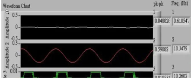
The high and low filter characteristics (Fig. 11-12) of electronic circuit hardware determined quality of the output signal. Inputting the 20 mV sinusoidal waves (low frequency) as bio simulation electronic signal to MEA chip (Fig. 8) verified the performance of MEA chip recording system (Fig. 13). Fig. 14 show the three channels recording result that channel 1 had no input signal and channel 2 have a exact waveform and amplification factor thorough this system (channel 3 was the origin input signal).
1 0 0 1 0 0 0 0 .1 1 1 0 Am pl itude ( V olt .) F r e q u e n c y ( H z )
Fig. 11 Low pass filter and cutoff frequency = 100 Hz
0 .1 1 1 0 0 .1 1 1 0 Amplitud e (Volt.) F re q u e n c y (H z )
Fig. 12 Low pass filter and cutoff frequency = 0.5 Hz
Fig. 13 Left picture show the recording system and right picture are the recording interface written by LabVIEW.
Fig. 14 The verification for the MEA recording System.
IV. CONCLUSION
In this report, we proposed a novel design planar MEA chip based on MEMS technology. The electrical properties
evaluated from MEA chip with 40 μm of microelectrode shown that this device provided good performance (impedance, phase) for bio signal detection in PBS. And the performance of detection system for signal acquisition had been evaluated and matched the monitoring requirement.
ACKNOWLEDGMENT
This project is supported by National Science and Technology Program in Pharmaceuticals and Biotechnology, National Science Council, Taiwan, R.O.C., NSC 92-2323-B002-001 and NSC 92-2323-B002-004.
REFERENCES
[1] P. Thi' ebaud, N. F. de Rooij, M. Koudelka-Hep, and L. Stoppini,“ Microelectrode Arrays for Electrophysiological Monitoring of Hippocampal Organotypic Slice Cultures”, IEEE Trans. Biomed. Eng., vol. 44, no. 11, pp. 1159-1163, Nov. 1997.
[2] P. Thi' ebaud, C. Beuret, M. Koudelka-Hep, M. Bove, S. Martinoia, M. Grattarola, H. Jahnsen, R. Rebaudo, M. Balestrino, J. Zimmer, and Y.Dupont, “An array of Pt-tip Microelectrodes for extracellular monitoring of activity of brain slices”. Biosensors & Bioelectronic,vol. 14, pp. 61-65, 1999.
[3] P. K. Campbell, K. E. Jones, R. J. Huber, K. W. H., R. A. Normann, “A Silicon-Based, Three-Dimensional Neural Interface: Manufacturing Processes for an Intracortical Electrode Array”, IEEE Trans. Biomed. Eng., vol. 38, no. 8, pp. 758-768 Aug. 1991.
[4] M. O. Heuschkel, M. Fejtl, M. Raggenbass, D. Bertrand, “A three-dimensional multi-electrode array for multi-site stimulation and recording in acute brain slices”, Journal of Neuroscience Methods, vol. 114, pp.D5 135–148, 2002. [5] S. Tatic-Lucic, Yu-Chong Tai, J. A. Wright, J. Pine and T.
Denison, ” Silicon-Micromachined Neurochips for In Vitro Studies of Cultured Neural Networks”, Technical Digest: International Conference on Solid-State Sensors and Actuators: Transducers ‘93, Yokohama, Japan, pp. 943-946, Nov. 1993.
[6] J. A. Wright, S. Tatic-Lucic, Yu-Chong Tai, M. P. Maher, H. Dvorak and J. Pine, “Towards a Functional MEMS Neurowell by Physiological Experimentation”, Technical Digest: ASME 1996 International Mechanical Engineering Congress and Exposition, DSC-Vol. 59, Atlanta, GA, pp. 333-338, Nov. 1996.
[7] U. Egert, H. Hämmerle, “Application of the microelectrode-array (MEA) technology in pharmaceutical drug research”, unpublished.