國
立
交
通
大
學
光電系統研究所
碩
士
論
文
非晶矽多接面太陽能電池模擬
Modeling of Amorphous Silicon Tandem Solar Cell
研 究 生:劉威麟
指導教授:林建中 助理教授
林健正 教授
非晶矽多接面太陽能電池模擬
Modeling of Amorphous Silicon Tandem Solar Cell
研 究 生:劉威麟 Student:Wei-Lin Liu
指導教授:林建中 Advisor:Chien-Chung Lin
林健正 Chien-Cheng Lin
國 立 交 通 大 學
光 電 系 統 研 究 所
碩 士 論 文
A ThesisSubmitted to Institute of Photonic System College of Photonics
National Chiao Tung University in partial Fulfillment of the Requirements
for the Degree of Master
In
Institute of Photonic System
July 2011
Tainan, Taiwan, Republic of China
I
非晶矽多接面太陽能電池模擬
學生:劉威麟 指導教授:林建中
林健正
國立交通大學光電系統研究所碩士班
摘要
在能源耗竭的現今,替代能源的發展已經是未來的趨勢,而在眾多替代能源 中,其中又以太陽能發電為最乾淨、環保、且取之不盡用之不竭的再生能源。所 以在發展各種不同種類的太陽能電池,我們選擇了非晶矽薄膜太陽能電池來做為 研究的主題。 薄膜太陽電池可以使用在價格低廉的玻璃、塑膠、陶瓷、石墨,金屬片等不 同材料當基板來製造,形成可產生電壓的薄膜厚度僅需數μm,因此在同一受光 面積之下可較矽晶圓太陽能電池大幅減少原料的用量,且薄膜電池太陽電池除了 平面之外,也因為具有可撓性可以製作成非平面構造,所以其應用範圍大,可與 建築物結合或是變成建築體的一部份。非晶矽薄膜太陽能電池在其效率上並不算 高,甚至比傳統的結晶矽太陽能電池還要來的低,但是由於在製程上完熟的技 術、具有可撓性、可以接合在建築材料上等種種優點,使的非晶矽太陽能電池的 研究還是非常熱門。 而這項研究主要著重於非晶矽材料用做薄膜太陽能電池的時候,有兩項不同 於其他太陽能電池的特點,一項是非晶矽材料的尾帶結構,另一項則是太陽能電II 池表面粗化的特色。而我們藉由了解尾帶結構的物理模型,模擬並分析非晶矽材 料由於尾帶結構造成的二次吸收,進而調整尾帶的參數來觀察各參數對於太陽能 電池的影響。而另一項對於表面粗化結構的模擬,我們建立兩種不同的表面粗化 結構。第一種是使用霧度公式添加到平坦的太陽能電池表面上,電池表面入射的 光會產生散射,從而達到表面粗化的效果。第二種方式則是參考真實的表面粗化 結構,並將此結構以座標的形式建立起一個類真實結構的平面,再藉由模擬了解 其粗糙面太陽能電池的特性。 而最後則是將表面粗化結構和尾帶結構兩者相結合並模擬,和實驗量測到的 數據來做擬合,增加模擬的準確性。建立一個模擬非晶矽薄膜太陽能電池,並且 具備一定準確性的平台是我們這項研究的目標。
III
Modeling of amorphous silicon tandem solar cell
Student:Wei-Lin Liu Advisor:Dr. Chien-Chung Lin
Dr. Chien-Cheng Lin
Institute of Photonic System
National Chiao Tung University
Abstract
Due to the depletion of energy resources, alternative energy development is the trend of the future. There are many alternative energy sources, and the solar power is a clean, environmentally friendly, renewable and inexhaustible one among them. Among several types of solar cells that are currently with high attention, we chose the amorphous silicon thin-film solar cells for the subject.
Thin-film solar cells can be produced on the substrates which could use
inexpensive glass, plastics, ceramics, graphite, or metal, and the film only needs a few μm to produce photo-generated voltages. So under the same light-receiving area, thin-film solar cell can significantly use less amount of raw materials than the conventional silicon solar cell. One of the important characteristics of thin film solar cells is flexibility. Its flexible properties can be applied to a wide variety of surfaces even combined with the building and window. Amorphous silicon thin-film solar cell does not surpass its crystalline counterpart for high efficiency. But due to several
IV
advantages such as mature manufacturing process, flexibility, and combined with the building materials, the amorphous silicon solar cell research is still very popular.
This research is focused on features which are different from other solar cells. One is the band tail structure of amorphous silicon materials, and the other is surface roughness. By studying the band tail physical model, we can devise the band tail absorption by tuning its parameters.
And another topic is the surface roughness. We create two different surface roughness of the structure. First we use haze formula to simulate the flat structure with haze by ideal situation. On the other hand, we established the real textured surface for simulating in order to achieve the real situation.
Finally, we combine the surface roughness and band tail in our simulation structure, and fitting the simulation results to the experimental data to enhance the simulation accuracy. Combination of these two features on a commercially available software is very important to expand our research for greater use. The accuracy of the simulation verified by the fitting process can ensure the validity of our band tail model and texture interface. We hope this application can be useful for design of the next generation thin film solar cell.
V
誌謝
在這碩士生涯的尾聲,終於到了要完成論文的階段了,回憶起這兩年來的種 種,最要感謝的人,當然還是指導教授林建中教授和林健正教授。那不厭其煩的 細心指導,讓我從土木跨入光電的領域,並能順利完成研究寫出這篇碩論,教授, 您辛苦了,非常的謝謝您。 此外,我還要感謝研究所的同學們,感謝神 PO 林智偉在我無聊時,陪我聊天 打屁,感謝實驗室同學謝奇穎,感謝對面實驗室的范承瑋,黃峻洋,林聖涵,黃 冠達,汪家陞,感謝橋對面實驗室的趙明義,感謝學弟黃禹軒,馬印聰,翁一正, 吳孟勳,還有有點麻煩但是也幫了我很多忙,帶給實驗室很多歡笑的學妹石謦 毓,還要感謝其它奇美樓三樓四樓五樓的同學、朋友們,感謝在研究所認識的好 朋友們,在我有困難的時候給予我幫助,度過了許許多多有歡笑有淚水的時光, 這份回憶一定會成為我生命中,最難忘的一部份,謝謝你們。 最重要的是特別感謝在背後支持的我的家人,你們讓我在求學期間一直無後顧 之憂,衷心的謝謝你們。 僅以此論文獻給我最親愛的家人與關心我的師長朋友,感謝你們的包容與愛 護,願與你們分享這份榮耀。 最後,要感謝的人實在太多了,還是就謝天吧!VI
Content
中文摘要
〃〃〃〃〃〃〃〃〃〃〃〃〃〃〃〃〃〃〃〃〃〃〃〃〃〃〃〃〃〃〃〃〃Ⅰ
Abstract
〃〃〃〃〃〃〃〃〃〃〃〃〃〃〃〃〃〃〃〃〃〃〃〃〃〃〃〃〃〃〃〃〃Ⅲ
誌 謝
〃 〃 〃 〃 〃 〃 〃 〃 〃 〃 〃 〃 〃 〃 〃 〃 〃 〃 〃 〃 〃 〃 〃 〃 〃 〃 〃 〃 〃 〃 〃 〃Ⅴ
Content
〃〃〃〃 〃〃〃 〃〃〃 〃〃〃〃 〃〃〃〃 〃〃〃 〃〃〃〃 〃〃〃〃 〃〃〃Ⅵ
List of figures
〃〃〃〃〃〃〃〃〃〃〃〃〃〃〃〃〃〃〃〃〃〃〃〃〃〃〃〃〃〃Ⅷ
List of tables
〃〃〃〃〃〃〃〃〃〃〃〃〃〃〃〃〃〃〃〃〃〃〃〃〃〃〃〃〃〃〃〃〃Ⅹ
Chap 1. Introduction
〃〃〃〃〃〃〃〃〃〃〃〃〃〃〃〃〃〃〃〃〃〃〃〃〃〃1
1-1 The advantage of solar cell
〃〃〃〃〃〃〃〃〃〃〃〃〃〃〃〃〃〃〃〃〃〃1
1-2 Types of solar cells
〃〃〃〃〃〃〃〃〃〃〃〃〃〃〃〃〃〃〃〃〃〃〃〃〃〃〃1
Chap 2. Thin film solar cell
〃〃〃〃〃〃〃〃〃〃〃〃〃〃〃〃〃〃〃〃10
2-1 Motivation
〃〃〃〃〃〃〃〃〃〃〃〃〃〃〃〃〃〃〃〃〃〃〃〃〃〃〃〃〃〃10
2-2 Theory
〃〃〃〃〃〃〃〃〃〃〃〃〃〃〃〃〃〃〃〃〃〃〃〃〃〃〃〃〃〃〃11
2-2-1 Physics of amorphous silicon alloy p-i-n solar cells
〃〃〃〃〃11
2-2-2 Tunnel junction
〃〃〃〃〃〃〃〃〃〃〃〃〃〃〃〃〃〃〃〃〃〃〃〃〃15
2-2-3 Haze
〃〃〃〃〃〃〃〃〃〃〃〃〃〃〃〃〃〃〃〃〃〃〃〃〃〃〃〃〃〃〃18
2-2-4 Band tail
〃〃〃〃〃〃〃〃〃〃〃〃〃〃〃〃〃〃〃〃〃〃〃〃〃〃〃〃〃20
Chap 3. Simulation and results discuss
〃〃〃〃〃〃〃〃〃〃〃〃〃26
3-1 Simulation software
〃〃〃〃〃〃〃〃〃〃〃〃〃〃〃〃〃〃〃〃〃〃〃〃〃〃26
3-2 Simulated structure
〃〃〃〃〃〃〃〃〃〃〃〃〃〃〃〃〃〃〃〃〃〃〃〃〃〃27
3-3 Band tail
〃〃〃〃〃〃〃〃〃〃〃〃〃〃〃〃〃〃〃〃〃〃〃〃〃〃〃〃〃〃〃〃29
3-4 Haze
〃〃〃〃〃〃〃〃〃〃〃〃〃〃〃〃〃〃〃〃〃〃〃〃〃〃〃〃〃〃〃〃〃〃33
VII
3-4-2: Ray tracing method
〃〃〃〃〃〃〃〃〃〃〃〃〃〃〃〃〃〃〃〃〃〃〃〃36
3-5: Fitting results discussion
〃〃〃〃〃〃〃〃〃〃〃〃〃〃〃〃〃〃〃〃〃〃〃39
Chap 4. Summary
& future work
〃〃〃〃〃〃〃〃〃〃〃〃〃〃〃〃〃〃〃42
Reference
〃〃〃〃〃〃〃〃〃〃〃〃〃〃〃〃〃〃〃〃〃〃〃〃〃〃〃〃〃〃〃〃〃〃〃43
VIII
List of Figures
Fig. 1-1 Types of solar cells. 〃〃〃〃〃〃〃〃〃〃〃〃〃〃〃〃〃〃〃〃〃〃2 Fig. 1-2 Monocrystalline solar cell. 〃〃〃〃〃〃〃〃〃〃〃〃〃〃〃〃〃〃〃〃
3
Fig. 1-3 Cadmium telluride thin film solar cell. 〃〃〃〃〃〃〃〃〃〃〃〃〃〃〃4 Fig. 1-4 CIGS device. 〃〃〃〃〃〃〃〃〃〃〃〃〃〃〃〃〃〃〃〃〃〃〃〃〃4 Fig. 1-5 Dye-sensitized solar cells. 〃〃〃〃〃〃〃〃〃〃〃〃〃〃〃〃〃〃〃〃6 Fig. 2-1 The IV characteristics of tunnel junction. 〃〃〃〃〃〃〃〃〃〃〃〃〃16 Fig. 2-2 Asahi U-type substrate (a) by AFM scan (b) by SEM scan. 〃〃〃〃〃〃20 Fig. 2-3 The density of state of a-Si. 〃〃〃〃〃〃〃〃〃〃〃〃〃〃〃〃〃〃〃21 Fig. 3-1 Light scattering at device simulation. 〃〃〃〃〃〃〃〃〃〃〃〃〃〃〃27 Fig. 3-2 Recombination rate at silicon solar cell. 〃〃〃〃〃〃〃〃〃〃〃〃〃〃27 Fig. 3-3 Simulated structure. 〃〃〃〃〃〃〃〃〃〃〃〃〃〃〃〃〃〃〃〃〃〃28 Fig. 3-4 Band gap of our simulated structure. 〃〃〃〃〃〃〃〃〃〃〃〃〃〃〃28 Fig. 3-5 The IV curve of tunnel junction (a) with voltage (b) on negative voltage. 〃29 Fig. 3-6 Band tails of amorphous silicon with different amplitudes. 〃〃〃〃〃〃30 Fig. 3-7 EQE with different amplitudes. 〃〃〃〃〃〃〃〃〃〃〃〃〃〃〃〃〃30 Fig. 3-8 Band tails of a- Si with different Lorentz resonant frequencies. 〃〃〃〃〃31 Fig. 3-9 EQE with different Lorentz resonant frequencies. 〃〃〃〃〃〃〃〃〃〃31 Fig. 3-10 Band tails of a-Si with different broadening parameters. 〃〃〃〃〃〃〃32 Fig. 3-11 EQE with different broadening parameters. 〃〃〃〃〃〃〃〃〃〃〃〃32 Fig. 3-12 EQE with different broadening parameters. 〃〃〃〃〃〃〃〃〃〃〃〃33 Fig. 3-13 Textured/Flat Device Comparison. 〃〃〃〃〃〃〃〃〃〃〃〃〃〃〃34
IX
Fig. 3-14 Light scattering at the flat structure in our simulation. 〃〃〃〃〃〃〃〃34 Fig. 3-15 The photogeneration rate when we added haze in our device. 〃〃〃〃〃35 Fig. 3-16 Flat and textured dual junction IV comparison. 〃〃〃〃〃〃〃〃〃〃36 Fig. 3-17 The different type rough surfaces. 〃〃〃〃〃〃〃〃〃〃〃〃〃〃〃〃37 Fig. 3-18 The cross section hight distribution of four types. 〃〃〃〃〃〃〃〃〃〃37 Fig. 3-19 This is the use of raytracing to create the rough structure. 〃〃〃〃〃〃38 Fig. 3-20 The EQE comparison of four different textured single junction cell. 〃〃38 Fig. 3-21 The IV of four different textured single junction cell at 10 suns. 〃〃〃〃39 Fig. 3-22 The ε2 we use to simulate. 〃〃〃〃〃〃〃〃〃〃〃〃〃〃〃〃〃〃〃40
Fig. 3-23 IV curve we simulated and fit with measured data. 〃〃〃〃〃〃〃〃〃41 Fig. 3-24 EQE comparison between we simulated and measured data. 〃〃〃〃〃41
X
List of Tables
Table. 3-1 The resistances of different tunnel junction doping concentration. 〃〃〃29 Table. 3-2 EQE peak direction with band tail parameters. 〃〃〃〃〃〃〃〃〃〃〃〃〃33 Table. 3-3 The solar cell parameters of simulation and experimentation.〃〃〃〃〃〃〃 40
1
Chap 1. Introduction
Energy technology innovation drove the evolution of human’s culture and promoted social development. However, with technological development, huge energy consumption for the environment we live also caused serious damage. So far the fossil fuel energy is used primarily to provide our current energy sources, but the environment caused by fossil fuel pollution: such as air pollution, global warming ... ... etc. These are serious issues, coupled with the increasing lack of oil stocks, and
Energy consumption also improved on, so the development of alternative energy sources, protecting the earth environment become the current issues of concern to everyone.
1-1 The advantage of solar cell
The use of sunlight is the cleanest, most environmentally friendly and inexhaustible renewable energy, Even if all the fossil fuels are exhausted, the sun will continue to supply new energy for mankind.
1-2 Types of solar cells
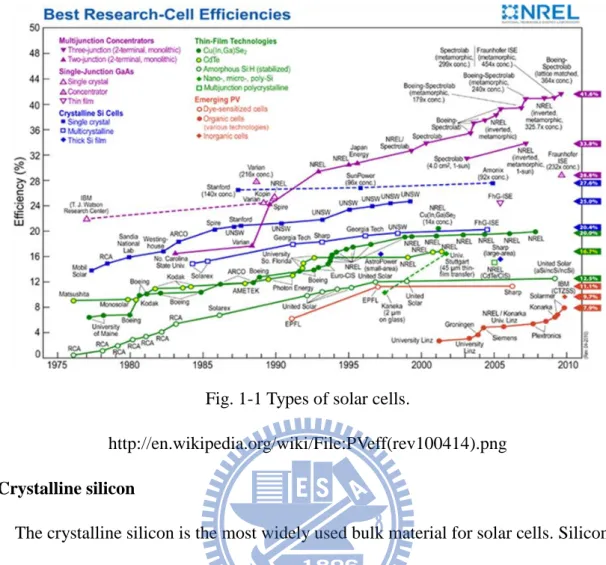
Today, there are many different types of solar cells. Therefore, we will give a brief introduction about their characteristics of the different types solar cells.
2
Fig. 1-1 Types of solar cells.
http://en.wikipedia.org/wiki/File:PVeff(rev100414).png
Crystalline silicon
The crystalline silicon is the most widely used bulk material for solar cells. Silicon is divided into several types according to the cause of the ingot or wafer of
crystallinity and grain size.
monocrystalline silicon (c-Si): The Czochralski process is usually used to made c-Si. Single-crystal wafers tend to be expensive and they are always cut from cylindrical ingots. It don’t fully cover a solar cell module which is square without wasting large amounts of refined silicon.
a. Therefore, c-Si panels have a problem that at the four corners of the cells is uncovered.
b. Poly- or multicrystalline silicon (poly-Si or mc-Si): The material of poly-Si is made from cast square ingots which are large blocks of molten silicon cooled
3
and solidified. The merits of poly-Si cells are less expensive to produce than conventional single c-Si cells, but the demerits are less efficient.
c. The other type of multicrystalline silicon is Ribbon silicon [1]:Its form is by drawing flat thin films from the molten silicon and then produce into a multicrystalline structure. This type thrift the production costs due to a great reduction in silicon waste, as this approach does not require sawing from ingots, but the efficiency is lower even than poly-Si.
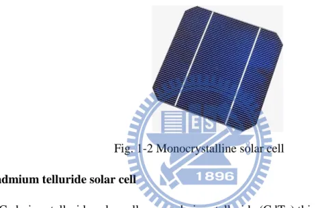
Fig. 1-2 Monocrystalline solar cell
Cadmium telluride solar cell
Cadmium telluride solar cells use cadmium telluride (CdTe) thin film
semiconductor layer to absorb sunlight and convert it into electricity. Since 2001, the best efficiency of the CdTe battery has stabilized at 16.5% [2]. Current increased has been almost fully developed, but more difficult challenge is junction quality,
performance and contacts CdTe has not been successful . Improved doping of CdTe and promote improved understanding of the key process steps (such as cadmium chloride recrystallization and contacting) is the key to progress. As in the single junction, CdTe is optimal in band gap choices. It may be expected that the efficiency of CdTe would be close to more than 20%. 15% of the module will then be possible.
4
Fig. 1-3 Cadmium telluride thin film solar cell
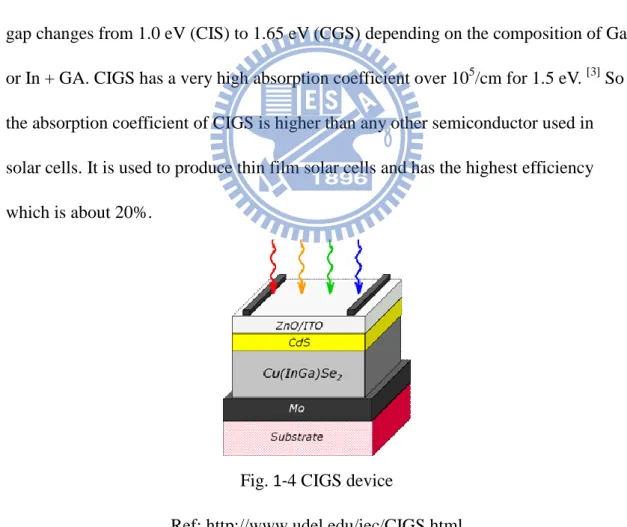
Copper-Indium Selenide
Copper Indium Gallium Selenide (CIGS) is a direct band gap semiconductor. Band gap changes from 1.0 eV (CIS) to 1.65 eV (CGS) depending on the composition of Ga or In + GA. CIGS has a very high absorption coefficient over 105/cm for 1.5 eV. [3] So the absorption coefficient of CIGS is higher than any other semiconductor used in solar cells. It is used to produce thin film solar cells and has the highest efficiency which is about 20%.
Fig. 1-4 CIGS device
Ref: http://www.udel.edu/iec/CIGS.html
5
Multi-junction photovoltaic cells are composed of multiple epitaxial layers. By using different alloys of III - V semiconductors, the band gap of each layer may be adjusted to absorb the specific ranges of electromagnetic radiation from sun, but each layer must be lattice matched and each cell needs to be current-matched. These matching criteria dominate the design and performance of the current multi-junction solar cell design.
Each layer of III - V solar cells has optical absorption in series which has the highest band gap material at the top. It receives the entire spectrum in the first junction. Then top layer with a higher band gap material will first absorb the shorter wavelength (i.e. higher energy) photons, and bottom layer will absorb photons which are transmitted through the top cell. [4]
Triple-junction cell consist of three different materials to absorbed the solar spectrum, for example, may consist of the semiconductors: GaAs, Ge and GaInP2. [5]
Each layer has their own band gap energy, so that can absorb different colors of light at each layer, or more precisely, absorb electromagnetic radiation over a portion of the spectrum. Semiconductors are carefully chosen to absorb nearly the entire solar spectrum, thus generating electricity from as much of the solar energy as possible.
All currently commercialized cells use a series circuit connection. This means that they are electrically connected in series and the composite cell has two terminals. A major constraint placed in tandem cells, as in series, current through each junction will be the same. If the maximum power point current of each junction is not the same, then the efficiency is affected. The current match of each junction is a very important design consideration for multi-junction cells.
6
GaAs-based devices are the most efficient multi-junction solar cells so far. By
October 2010, the triple junction metamorphic cell reached a record high of 42.3% . [6]
Light-absorbing dyes (DSSC)
The dye-sensitized solar cell (DSSC's, DSC or DYSC) is a type of thin-film solar cells. Different from classical thin-film cells in the light absorption of semiconductor layer, a absorption occurs in dye molecules adsorbed at a highly porous structure of nano-particles of transparent TiO2 like Fig. 4. Dye excitation is followed by electron
injection into the TiO2 and by dye re-charging via a redox electrolyte (mostly I-/I3-).
Electrons are delivered to the front of the contact in the titanium dioxide nanoparticles which are a transparent conductive oxide (TCO). The contact with the redox
electrolyte is made by a back contact (catalyst coating). For backside illumination, it can also be made the TCO transparent window as a contact. [7]
Fig. 1-5 Dye-sensitized solar cells. [8]
Dye-sensitized solar cells are a class of low-cost solar cells belonging to the group of thin film solar cells. It’s operation is based on a semiconductor formed between a photo-sensitized anode and an electrolyte just like a photoelectrochemical system. This cell was invented by Michael Grätzel and Brian O'Regan at the É cole
7
Although the efficiency of Dye-sensitized solar cells is less than 11%, but more research is confident that efficiency can be improved.[9]
Organic/polymer solar cells
Organic photovoltaic cells (OPVC) are the photovoltaic cells using organic
electronics. The light absorption and charge transfer of organic photovoltaic cells are related with small organic molecules or conductive organic polymers.
Plastic has a lower cost of production in high volumes. Combined with the flexible organic molecules, that makes it potentially lucrative for photovoltaic applications. Molecular engineering such as changing the length and functional groups of the
polymer can change the energy gap, which makes chemical changes in these materials. The optical absorption coefficient of organic molecules is high, so a lot of light can be absorbed by a small amount of material. The main disadvantages of organic
photovoltaic cells are low efficiency, low stability and low intensity compared to inorganic photovoltaic cells. [10]
Polymer solar cells and organic solar cells are created from thin films (typically 100 nm) of organic semiconductors which include polymers, such as small-molecule compounds like copper phthalocyanine, polyphenylene vinylene, carbon fullerenes and fullerene derivatives. Energy conversion efficiency achieved to date using conductive polymers is low compared to inorganic materials. However, it improved rapidly in the past few years; the highest efficiency from NREL (National Renewable Energy Laboratory) achieved 6.77% [11]
The advantages of organic solar cells are better economic factors such as lower production cost and lower material costs than conventional solar cells obtained by
8
forming a PN junction on the single crystal such as silicon, germanium. In order to attract attention, In recent years, the organic solar cells has been improved their disadvantages and developed the usage of a solar cell application for general public.
Silicon thin films
Thin-film solar cells can reduce the use of amount of material due to the
development of thin-film technology. This can reduce the cost of materials and energy conversion efficiency. The silicon thin-film solar cell has become popular due to its cost, flexibility, lighter weight, and easy to integrate (compared to wafer silicon cell). Silicon thin-film solar cells are deposited by chemical vapor deposition (typically plasma-enhanced (PE-CVD)) from silane gas and hydrogen gas. Depending on the process parameters, this can yield:[12]
1. Microcrystalline silicon (μc-Si or μc-Si:H) 2. Amorphous silicon (a-Si or a-Si:H)
3. Protocrystalline silicon
It has been found that protocrystalline silicon has the high open circuit voltage in the low volume fraction of nano-silicon.[13] These types of silicon assist dangling bonds which cause some defects like energy levels in the band gap as well as deformation of the valence and conduction bands . The solar cells made from these materials have lower conversion efficiency than crystalline silicon, but production costs are also less than the conventional solar cells. The quantum efficiency is also lower, because it decrease the number of collected charge carriers per incident photon.
The band gap of amorphous silicon is about 1.7ev which is higher than the
9
part of the solar spectrum more strongly than the infrared portion of the spectrum. A-Si usually combined with μc-Si into tandem cell, due to the μc-Si has the same band gap as the crystalline silicon which can absorb the part of infrared spectrum. So the top of tandem cell is a-Si which can absorb visible light and leaves the bottom of the cells in the μc-Si infrared part of the spectrum.
The mainly research of this paper are the simulation of thin film amorphous silicon solar cells and discussion of the results.
10
Chap 2. Thin Film Solar Cell
2-1 Motivation
There are several advantages of thin film solar cells. Solar cell with flexible substrate is the forerunner of the photovoltaic energy. Costs for this technology are dropping quickly and with the investment in research and development, these costs will continue to fall. The biggest advantages with thin film solar cells are their various application options. Unlike traditional panels, flexible panels can be applied to a wide variety of surfaces. In addition to the traditional roof mounted design, these cellscan be placed in the transportation vehicles, in the building surfaces, and even in the daily goods. Under low-light condition (such as cloudy sky, bright moon light, etc.), thin film solar cell is better than the crystalline silicon cell. Thinfilm solar cells do not require the glass and aluminum casings of traditional cells because the materials within them are flexible and ductile. This means they will likely take more abuse and last longer.[14]
Why do we chose amorphous silicon? Because silicon is the second most abundant material on earth, and its light absorption layer thickness can be thin and still be effective. Also it is more mature in manufacturing process. Therefore, amorphous silicon is still one of the prominent candidates for thin film solar cell technology.
Amorphous silicon material used in the thin film solar cell has two unique features, the first is the band tail. Due to its disordered lattice points and extra defects in the material, amorphous silicon has a tail of density of states extended into forbidden gap region. The second is interfacial roughness. This comes from the thin film cell
11
topics need to be considered for modeling.
Finally, our goal is to create a platform which includes the following characteristics, easily accessible, accuracy in electrical and optical properties, .and possible future improvement for device.
2-2 Theory
In our simulation calculation, several aspects of the amorphous silicon solar cell needs to be covered. They are basic carrier drift-diffusion model of amorphous silicon alloy p-i-n solar cells, tunnel junction, haze, and band tail models. We will discuss these topics as follows.
2-2-1 Physics of amorphous silicon alloy p-i-n solar cells
Many efforts have been done to properly model the amorphous silicon p-i-n structure [15]. We will follow the model from ref. 15 closely in the next few sections. Our simulation is based on the solution of the electron and hole continuity equations:
) ( ) ( 1 x R x G dx dj q n (2-1) ) ( ) ( 1 x R x G dx dj q p (2-2)
where G is the generation rate and R is the recombination rate. Poisson’s equation is
(x) dx d (2-3)
, where is the electric field inside the device. The electron and hole conduction current densities are
) ( dx dn q KT n q jn n (2-4)
12 ) ( dx dp q KT p q jp p (2-5)
μn is the band mobility of electrons and μp is the band mobility of holes, T is the
sample temperature, and ε the dielectric constant of amorphous silicon.
We can then calculate the recombination rate R(x) and charge density ρ(x) by considering the electron and hole concentrations and the distribution of localized states g(E) in the mobility gap.
) ( ) ( ) (E g E g E g D A (2-6) ] ) ( exp[ ) ( min D mc D D E E E g E g (2-7) ] ) ( exp[ ) ( min A mc A A E E E g E g (2-8)
where EA and ED are the characteristic energy slopes of exponential distributions of
acceptor- and donor-type localized states and Emc is the energy difference between the
minimum in the density of states and the conduction band edge.
And then we assumed the densities of states to be the same as for crystalline silicon of their conduction band and valence band. In particular, there is experimental
evidence that the existence of defect band associated with dangling bonds is at around 1eV below the conduction band edge.[20] Discussed in Ref [21], it affects values of undoped samples, for gmin=1016cm-3eV-1.We assume
min min min 2 gA gD g (2-9)
We can model the effect of dopants on the density of states spectrum as it is well known that small quantities of dopants introduce new states into the gap.[16]
13
Some experimental evidence shows that the dopant-created defect density is proportional to the square root of the dopant density [17] and the density of states:
) 0 ( ) 0 ( ) ( min min min N g N K N g N g (2-10)
where N=total dopant concentration, K a suitable constant, and gmin(N=0)=1016
cm-3eV-1. Using the model [18] which is a detailed analysis of amorphous silicon under the steady-state photoconductivity phenomenon, and for the K value, we use an appropriate value of K tobe equal 3×1016 cm-3eV-1.5.
The space-charge density ρ (x) described as
)
(
)]
(
)
(
[
)
(
x
g
x
n
x
Tx
(2-11) where)]
(
)
(
)
(
)
(
[
)
(
x
g
p
tx
n
tx
N
Dx
N
Ax
T
(2-12)Here pt(x) and nt(x) are the concentrations of trapped holes and electrons,
respectively, ND+(x) and NA-(x) are the ion concentrations of shallow donors and
acceptors.
The concentrations of Pt and Nt is defined as the electron and hole trap quasi-Fermi
levels positions.[19]
For acceptor-like states these are given by
)
ln(
c c a tnN
Cp
n
KT
E
E
(2-13))
/
ln(
v v a tpN
C
n
p
KT
E
E
(2-14)14
)
/
ln(
c c d tnN
C
p
n
KT
E
E
(2-15))
ln(
v v d tpN
nC
p
KT
E
E
(2-16)Where NC and NV are the density of states in the conduction band and valence band,
and EC and EV are the energy corresponding to the conduction band bottom and the
top of the valence band, and
N C
C
(2-17)where σC is the cross section of a charged trap and σN is the cross section of a neutral
trap.
We use the zero-temperature distribution function to calculate the density of trapped electrons and holes. The results underestimate the trapped electron density, but it has not manifest error, provided the characteristic energy density of the slope of EA and ED is greater than KT.
In this approximation donor-like trap probability occupied by electron is
d tp v d tn d tp c d tn
E
E
E
E
E
E
E
E
E
p
nC
nC
f
1
0
(2-18)and for acceptor-like traps it is
a tp v a tn a tp c a tn
E
E
E
E
E
E
E
E
E
Cp
n
n
f
1
0
(2-19)15
a tn a tp a tp v E E A E E A tg
E
dE
Cp
n
n
dE
E
g
n
(
)
(
)
(2-20)
d tn d tp d tn c E E D E E D tg
E
dE
p
nC
p
dE
E
g
p
(
)
(
)
(2-21)And then, we use the Shockley-Read recombination model to find the carrier recombination and the rate R(x) is
d tn d tp a tn a tp E E D E E A n i ng
E
dE
p
nC
dE
E
g
Cp
n
C
n
p
x
R
(
)
1
(
)
)
(
1
(
)
(
)
(
2
(2-22)where ni is the intrinsic carrier concentration, ν is the thermal velocity, and (np-ni2 ) is
driving force of recombination. [22]
In the simplest condition, the generation rate G is
x
e
G
x
G
(
)
0
(
)
() (2-23) where G0 is the incident photon flux of wavelength λ, α(λ) is the absorptioncoefficient, and x is the distance from the top of the cell. Then, we consider the more realistic model of generation rate including the actual back reflection in amorphous silicon solar cells.
)
(
1
)
(
)
(
0 x x Te
Pe
P
G
x
G
(2-24)where P is a transmission factor for light traveling twice through the cell. Equations (2-1~2-24) are our considered model.
2-2-2 Tunnel junction
16
some film layers generated by molecular beam epitaxy or metal organic chemical vapor deposition. These films are composed of different semiconductors with different band gap characteristics, which can absorb the energy gap in a specific frequency spectrum of electromagnetic energy. The multi-junction solar cell generated by special design of semiconductor can absorb most of the frequencies of sunlight to generate more energy. [23]
Now, the solar cell had the best efficiency is use multiple p-n junctions, each layer tuned to absorb a specific frequency spectrum. Due to the light has a strong reaction on the structure layers which are the same size as wavelength, so they can absorb the lower frequency of light as long as these layers are extremely thin. This makes layers be stacked; the top layer absorbs the high frequency of light, and the bottom layer absorbs the lower frequency of light. The layers would be made of different materials and connect them by tunnel junction.
Fig. 2-1 The IV characteristics of tunnel junction.[24]
The main purpose of the tunnel junction is the connection between the two subcells to provide a low resistance and low optical loss. Without it, the top p-doped region of
17
the cell directly connected to the middle subcell n-doped region. Thus, the
photovoltage would become lower. To reduce this effect we used the tunnel junction to be a connection. [25] It is a simple wide-band, high-doped diodes. High doping would reduce the depletion length, because
D A D A depl N N N N q V l 2(0 ) (2-25)
Therefore, the electron can easily tunnel through the depletion region. The IV characteristic of tunneling junction is very important (as shown in Fig. 2-1) because it explains why the tunneling junction can be used as a low resistance to the pn junction connection. The region that the electron tunnels through the battery is called tunnel region. There, the voltage must be low enough so that some of the electrons can tunnel to the other side. Consequently, the current density through the tunneling junction is high. Then, the resistance is very low, so the voltage is, too. This is why the tunnel junction is an ideal connection for PN junction without voltage drops. When the voltage is high, electrons cannot cross the barrier, because the electronic energy state is no longer applicable. Therefore, the current density decreased and the differential resistance is negative. The last region, known as the thermal diffusion region is corresponding to the normal diode IV characteristics:
) 1 ) (exp( kT qV J J S (26)
In order to avoid impact the performance of muti-junction solar cell, the tunnel junction design in the absorption of wavelength must not be influenced the next photovoltaic cell, middle cell, i.e. EgTunnel > EgMiddleCell.
18
2-2-3 Haze
Light scattering in thin-film silicon solar cell is an important feature, usually by the rough surface of the structure to achieve this effect. Transparent front contact material of the solar cells develops their texture in the growth process or in the subsequent etching step. The back contact metal of the cell would have an appropriate surface texture due to the deposition technology. The optical properties of light scattering, reflection, and transmission can start from this metallic surface.
In the interface of rough surface, light transmission and reflection are mainly composed by these two parts of specular part and diffusion. The rough surfaces theory of light scattering can be traced back to the reflection such as radar from the land surface. The model of textured surface is considered the scalar or vector under the influence of polarization, but the surface roughness of the structure size, either root mean square (rms) roughness, or its correlation length is usually assumed to be smaller than the wavelength λ. However, the thin-film silicon solar cells which has refractive index of silicon (nSi) be usually 3.5 and 4 can absorb the wavelength λ in a
large range from 300 to 1100 and effective absorption wavelength is λeff=λ/nSi .
In the early model, roughness was usually assumed to follow Gaussian distribution and its standard deviation can be correlation length. The root mean square roughness is also used to define as the rate of roughness. The particular point is haze which is a quantity defined as the reflection and transmission by the ratio between diffused light and total intensity. Haze's relationship as given in the following formula, using Carniglia notation, [26] } ] cos 2 ) / 2 [( exp{ 1 / total rms 1 i 2 diffuse R R R n H (2-27)
19 } ] ) ( 2 ) / 2 [( exp{ 1 } ] cos cos 2 ) / 2 [( exp{ 1 / 2 1 2 2 1 T rms t i rms total diffuse T c n n n n T T H (2-28)
In these two equations, θi and θt represent the angle of the incident and the angle of
the specularly transmitted beam, respectively, measured with respect to the surface normal. The refractive index of the incident medium is denoted by n1, n2 is the
refractive index of the medium into which light is transmitted. The wavelength and the root mean square roughness are denoted by λ and σrms, respectively.[27]
And by our simulation, we use the fixed haze function about the Asahi U-type TCO. Fig. 2-2 are the surface scan picture. Using the scalar scattering theory [28] the relation between σrms and HT is given by the following formula:
] ) / 2 ( exp[ 1 ) / (T T n0 n1 2 HT diffuse total rms (2-29)
Here Tdiffuse is the diffuse transmittance, Ttotal is the total transmittance, n0 and n1 are
the refractive indices of first and second media and λ is the wavelength. As the simulations with the equation (2-29) do not provide good agreement with the measured values of HT for Asahi U-type TCO, we used a modified formula [29] as
follows: ] ) / 4 ( exp[ 1 Cn0 n1 3 HT rms (2-30) In this formula C is a factor that depends on the two media and we assumed C =1 and σrms =20nm in our simulation.
20
Fig. 2-2 Asahi U-type substrate (a) by AFM scan (b) by SEM scan. [30]
2-2-4 Band tail
Amorphous silicon has three principal features which are the short range order of the ideal network, the long range disorder and defects. The abrupt band edges of a crystal like Fig. 2-3 which are replaced by a broadened tail of states extending into the forbidding gap originates from the deviations of bond length and bond angle arising from the long range structure disorder.
The band tail plays an important role in amorphous silicon that carriers can transport at this band edge. So it would affect some electronic properties by controlling trapping and recombination. From the past experiments, it is very clear that the band tail are approximately an exponential distribution. Many assumptions have been used to explain this phenomenon. Some models pointed out that the optical absorption which would have the exponential edge. Other models are considered as electron-phonon interactions or thermodynamic equilibrium occupancy of the different possible configurations. Therefore, there are many different ways to make the tail be established.[31]
21
Fig. 2-3 The density of state of a-Si.[31]
Almost 30 years ago, Tauc modeled the tail about the amorphous material. They made the following assumptions:[32]
Assuming the volume V in the amorphous contains the same number of atoms as in the crystalline state and we neglect the difference of densities of both states.
It is known from experiment and theory that the amorphous has its own conduction and valence band. We assume to describe the change of the crystalline state into amorphous state by perturbation theory. The amorphous valence band wave functions is in zero approximation linear combination of the crystal valence band wave function; conduction band can also be described by the same way.
Therefore, the ground state described by Slater determinant is as the same as in the crystal. If we now generate electron-hole pairs in the crystal wave function and their wave functions are x , cx , and then use the perturbation we obtain the wave ' functions in amorphous solid to calculate. We can label these wave functions
a
x
,
a
cx' with indices x , 'x . As the perturbation is on the continuous spectrum, we can
assume that state
a
x
22
the same (conduction band described on the same way as valence band). As a result, these assumptions corresponding densities of states are the same in both cases. We start from the general one-electron formula:
) ( 1 ) 2 ( ) ( 2 , 2 2
f i f i if E E P V m e (2-31)where the i, f are the initial and final states and V is the basic volume. Pif is the
momentum matrix element between the wave functions of the final and initial states
a
cx' and
a
x
. In the respective bands, describing them by linear combinations of Bloch functions, we obtain:
) ( ' ' ' ' ' ' k P x k ck cx k P ck x k ck cx x P cx P vc a k a k a k a a a if
(2-32) where )] ( [ ) ( 1 ) (k i d3ru* r grad u r P ck cell k vc
(2-32)is the matrix element of the crystal. Summations over all k vectors perform in the first Brillouin zone. Ω is the basic unit cell’s volume in which the integration is performed From (2-31) we obtain ) ( ) ( 1 ) 2 ( 2 ) 2 ( ) ) ( ( ) ) ' ( ( ' 1 ) 2 ( 2 ) 2 ( ) ) ( ) ' ( ( ) ' , ( ' 1 ) 2 ( 2 ) 2 ( ) ) ( ) ( ( ) ( ) 2 ( 2 ) 2 ( ) ) ( ) ' ( ( ' ) ( 2 ) 2 ( ) ( 2 0 3 2 3 3 2 0 3 2 3 3 2 3 2 2 3 3 2 ' 2 2 2 E g E g dE P B m e x E E x d E x E x d dE P B m e x E x E x x f x xd d P B m e x E x E x P x d m e x E x E x k ck cx k P V m e v c vc v c vc B v c vc B v c vc v c x x k a a vc
(2-33)23
The summations are over all χ, χ’ in the first Brillouin zone. In a crystal, we get
kx kx vk vx ck cx' ', (2-34) and ' 2 ' ' ) ' , ( xx k a a cx ck vk vx N N x x f
(2-35) ) ' , (x xf would have a maximum for xx' and a certain width which is non-zero in
an amorphous material. And we can find the relationship: d3xd3x'f(x,x') B2
B
(2-36)B is the volume in the reciprocal space of the Brillouin zone.
We now discuss a particularly simple example that f(x,x') is a constant ( f0) as xx'0in the certain part of the Brillouin zone Bo and zero in the rest.
Obviously, ε2(w), is a convolution of the density of states in the conduction band
and valence band gc(E) and gv(E) for its energy is conserved. If we can measure the
energies from the band extrema we have: g p n n n c p p v E E g E E E E E g ( )~ 1/2, ( )~ 1/2, . We obtain then from (2-33)
2 2 2 ) ( ~ ) ( Eg (2-37) The imaginary part of the dielectric function above the band edge, we can show that:
2 2 2(E) AT(EEg) /E
(2-38) where AT and the optical band gap Eg are the two constants which need to be fit.
And then, the new parameterization is obtained from the Tauc joint density of states (2-38) and the standard quantum mechanical or Lorentz calculation for ε2 of a
24
collection of non-interacting atoms. If only a single transition is considered, ε2(E) is
given by 2 2 2 2 0 2 0 2 ) ( 2 ) ( E C E E CE E A nk E L (2-39)
where E0 is the peak transition energy and C is the broadening term.
If the ε2(E) from (2-39) is connect with (2-38), one obtains
g g g TL E E E E E E C E E E E C AE E 0 ] 1 ) ( ) ( [ ) ( 2 2 2 2 0 2 2 0 2 (2-40)
This physic model TL is based on the Tauc joint density of states and the Lorentz oscillator; the four parameters, Eg is the band gap energy, A is the amplitude, E0 is the
Lorentz resonant frequency and C is the broadening parameter.[33]
But in our simulation, we use the modified band tail model which is Tauc-Lorentz dielectric function combined with the exponential Urbach tail. This model is the most widely to analysis the band tail of amorphous material.
c c u u g E E E E C E A E E E C E A A E C E E E E C AE E E 0 ) ) , , ( exp( ) , , ( ) ( ) ( 1 ) ( 0 0 2 2 2 2 0 2 2 0 2
(2-41)The first term (E> EC) is the same as the Tauc-Lorentz function and the second term
(0 <E <EC) is used to describe the Urbach tail.
Au and Eu are respected the continuity of optical function including first derivative. This relationship is expressed as:
25 1 2 2 0 2 2 2 2 0 2 2 ) ( ) ( 2 ) ( 2 2 ) ( E E E C E E C E E E E E E c c c g c c g c u (2-42) and 2 2 0 2 2 2 2 0 ) ( ) ( ) exp( E E E C E E C AE E E A c c g c u c u (2-43)
The real part ε1 of the complex dielectric function
2 2
1i (nik)
isobtained using analytical integration of the Kramers-Krönig relation.[34] Therefore, by matertial absorption calculation:
k
4 (2-44)The decay coefficient K can be expressed as:
] [ 2 1 2 2 2 1 1 2
k (2-45)26
Chap 3. Simulation and Results Discuss
In this section, we will demonstrate our simulation results by combining the aforementioned theories and models. The experimental data will be fitted with the commercial available software (Silvaco Atlas® ). First we build a tandem dual junction solar cell. We cascade two cells through a highly doped p-n tunnel junction. A single junction solar cell is also built for later verification purposes.Second, we change the band tail parameters of Tauc-Lorenz dielectric function with the
exponential Urbach tail, and discuss the band tail and EQE relationship. Finally, in order to simulate the real textured structure, we find four different rough surfaces and use Matlab® to intercept the surface height distribution, and then we create the four different types surfaces of solar cells. We observe and discuss the different types solar cells according to simulation results.
3-1 Simulation Software
We used software is called TCAD® by corporation Silvaco®. and use the modular Atlas® to do device simulation. Atlas® enables device technology engineers to
simulate the electrical, optical, and thermal behavior of semiconductor devices. Atlas include many different device simulators like S-Pisces and Luminous.
27
Fig. 3-1 Light scattering at device simulation.
Fig. 3-2 Recombination rate at silicon solar cell.
3-2 Simulated Structure
Our simulated structure of the above material is amorphous silicon and we use tunnel junction to connect the bottom layer which is micro crystalline silicon. ( as shown in Fig. 3-3)
28
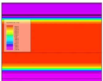
Fig. 3-4 Band gap of our simulated structure.
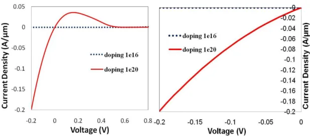
The first thing we need to deal with is the right tunnel junction design. It is important for a tandem cell to have a good tunnel junction. Fig. 3-4 is our simulated structure band gap. And the middle of a very narrow part is the tunneling junction. We tuned the different doping concentration of p+ and n+ layer. We simulated their IV curve (as shown in Fig. 3-5) and calculated their resistances. When on negative bias, the tunneling junction can be seen as a resistance. We calculated their resistances like Table. 3-1.
29
TJ doping concentration (cm-3) Resistance (Ω)
1e20 1.046704
1e16 5.00E+11
Table. 3-1 The resistances of different tunnel junction doping concentration The resistance of doping concentration 1e20 is much smaller than the resistance of doping concentration 1e16. We can see when doping concentration higher the
resistance will become lower. And then, we tried doping concentration 1e21, but it would error. Doping concentration is too high not only in the manufacturing process would be difficult, the simulation which refer to an ideal model to calculate would be no convergence on the results.
3-3 Band Tail
After we have a tunnel junction and IV calculation finished, we can focus on the band tail and EQE relationship. We devise a single junction cell to test the effect of band tail towards the EQE. we tuned amplitude, the Lorentz resonant frequency, the broadening parameter, and simulated their EQE.
30
Fig. 3-6 Band tails of amorphous silicon with different amplitudes.
Fig. 3-7 EQE with different amplitudes.
At first, the greater amplitude would cause the higher ε2 like Fig. 3-6. The top line
had the highest amplitude and it would cause the highest ε2. According to the theory
previously mentioned, the band tail with the greaterε2 would have the better
absorption.
So it would cause higher External quantum efficiency as shown in Fig. 3-7.
31
Secondly, the Lorentz resonant frequency would change the band tail’s shape. We set the higher value would cause the lowerε2, by reference to the physical model of
this result is to be expected. And then, we compared the other two different value, E0=3.02 had a higherε2 in the long wavelength and E0=4.02 was higher in the
short-wavelength.
Fig. 3-9 EQE with different Lorentz resonant frequencies.
The absorption of different band tail distribution showed out on the EQE results. E0=8.02 had the lowest EQE. E0=4.02 had the greater performance in the
32
Fig. 3-10 Band tails of a-Si with different broadening parameters. Last, we tuned the broadening parameter. C=0.99 had a higher peak in the short-wavelength, and C=4.99 was in the long-wavelength.
Fig. 3-11 EQE with different broadening parameters.
According to the result, the band tail had a greater impact on long-wavelength absorption.
Band tail
parameter
A
↑
E0
↑
C
↑
EQE peak
direction
↑
↙
↗
Table. 3-2 EQE peak direction with band tail parameters.
3-4 Haze
Why create rough surface? Thin film hydrogenated amorphous silicon (a-Si:H) solar cells can be applied in various conditions with great varieties of forms.
33 θ0
θ1 θ0
θ1
Fig. 3-12 EQE with different broadening parameters.
In this structure, we could diffuse the incoming light, and it could increase the light path in the cell. So light absorption would enhance by more light trapping.
Two different ways can describe this scattering phenomenon in our simulation. We created two different rough surface structures like Fig. 3-13. First, we can use an ideal scattering function at the specific interface to simulate structure. So the interface is still flat. It’s easy to implement and simulation process would be faster. The other method is create the real texture, and using ray tracing .We use actual peaks and valleys for interface and follow the geometrical optics theory in the micro scale. But it is slower in calculation and we can obtain localized result.
Fig. 3-13 Textured/Flat Device Comparison.
3-4-1: Interface Diffusion Function
We use the software built-in features which can make light scattering. This function can be achieved similar to the effect of surface roughness.
34
Fig. 3-14 Light scattering at the flat structure in our simulation.
The connection between the specular and diffused portions of the light is described by haze functions we mentioned on the Chapter 2: Haze theory.
In the software, these two formula are the transmissive haze function HT (3-1) and the
reflective haze funciton HR (3-2), and the root mean square roughness we used to
simulate is 20nm. ] ) ) cos( 2 ( exp[ 1 1 2 3 n n HT (3-1) ] ) ) cos( 4 ( exp[ 1 1 2 n HR (3-2)
35
Fig. 3-15 The photogeneration rate when we added haze in our device.
From the simulation results (as shown in Fig. 3-15), the photogeneration rate would increase when we added the light scattering. So the higher photogeneration rate would have the more carrier transport to the electrode. From the simulation results (as shown in Fig. 3-16), we can see a trend that the textured surface performance is better than the smooth structure.
However, the simulated conditions is too ideal. So the trend of the simulation results as a reference, but we still requires experimental measurements to verify our simulation.
36
Fig. 3-16 Flat and textured dual junction IV comparison.
3-4-2: Ray Tracing Method
Using the diffusing interface is easy but too ideal. In order to simulate the real case, we need to input the actual textured profile into software. We find four different rough surfaces[27] and use matlab to intercept the surface height distribution. Fig. 3-17 is four different rough Surface we used.
37
Fig. 3-17 The different type rough surfaces.
We use matlab to intercept these four type rough surfaces. Fig. 3-18 is the cross section hight distribution of four types.
38
Fig. 3-19 This is the use of raytracing to create the rough structure. We can see the light transmission path at the rough structure and the refraction of different wavelengths on Fig. 3-19.
Next, we simulated these four textured surfaces and compared with the flat surface structure. (as shown in Fig. 3-20 and Fig. 3-21)
39
Fig. 3-21 The IV of four different textured single junction cell at 10 suns. Due to the complexity of calculation, this method is more machine-resources emanding. So we used single junction to simulate these four textured structure that could be faster than simulated dual junction. In our simulated results, type C had the best performance in EQE and IV curve. And in these results, we could see that the textured surface had the better performance than flat surface of thin film solar cell.
3-5: Fitting Results Discussion
Finally we need to check with the real measurement data.We combined the previously mentioned haze and band tail simulation. The parameter we used were: amplitude :136
Lorentz resonant frequency: 4.02 broadening parameter :2.99
40
Fig. 3-22 The ε2 we use to simulate
Next, we used the interface function to simulate the flat surface with textured. This design could enhance the computing speed when we simulated the dual junction with tunnel junction. So we got the result to fit the measured data that provided by ChiMei energy.
The IV comparison of the device, solid line is our simulation and broken line is measured result. We can clearly observe that the two lines are very close. The some important parameters of solar cell we showed on the Table. 3-2.
Parameters
Experimental data
Simulation
I
sc(mA)
10.08
10.11
V
oc(V)
1.2697
1.272
P
m(mW)
8.206
8.861
FF
0.646624
0.655884
41
From experimental result, we can see the IV curve is not an ideal diode. So the FF is just 0.65. We added some defect density to fit it and simulated the EQE (as shown in Fig. 3-24) of this device with the same conditions. Amorphous silicon absorbed in the short-wavelength, and in the long-wavelength is micro crystalline silicon. Because the amorphous had a bigger band gap than micro crystalline silicon. According to the result, the amorphous silicon part can be seen very close to our simulation.
Fig. 3-23 IV curve we simulated and fit with measured data.
42
Chap 4. Summary
& Future Work
We construct a commercially viable model for a dual junction, textured surface a-Si:H solar cell, and our calculation agrees with experimental results well.
Through the analysis of the band tail characteristics, we can understand the change of absorption spectrum in amorphous Si and its effect on the EQE. And then, both diffusing interface and actual texture surfaces are applied to the amorphous silicon solar cell, and both shows enhanced photogenerated currents. So the current platform of amorphous silicon solar cell should be useful for the optimization of next
generation solar cell.
In future research, we would like to add the solar cells measured results of rough surface and smooth surface to fit our simulation much better, and creating a better accuracy of the simulation platform. And then, we will design the structure for different rough layer and adjust the parameters of thin film solar cell (such as thickness of the doping, corresponding defects due to roughness, etc.) to achieve improved efficiency and better performance.
43
Reference
1. D.S. Kim et al, "String ribbon silicon solar cells with 17.8% efficiency", Photovoltaic Energy Conversion, 2003., Vol.2, 1293 - 1296.
2. X. Wu et al. (October 2001), " High Efficiency CTO/ZTO/CdS/CdTe
Polycrystalline Thin Film Solar Cells", NREL/CP-520-31025.
3. Billy J. Stanbery, “Copper Indium Selenides and Related Materials for
Photovoltaic Devices”, Critical Reviews in Solid State and Materials Sciences,
27(2):73–117 (2002).
4. D. J. Friedman et al, “GalnPiGaAs Monolithic Tandem Concentrator Cells”, Photovoltaic Energy Conversion, 1994., vol.2, 1829 - 1832.
5. Spectrolab, ” Triple-Junction Terrestrial Concentrator Solar Cells”, spectrolab Inc. , http://www.nrel.gov/awards/2001_triple_junction.html
6. “Spire pushes solar cell record to 42.3%”, Optics.org. Retrieved on 2011-01-19. 7. "Dye-Sensitized vs. Thin Film Solar Cells", European Institute for Energy
Research, 30 June 2006, http://www.eifer.uni-karlsruhe.de/.
8. Brian O'Regan et al, "A low-cost, high-efficiency solar cell based on dye-sensitized
colloidal TiO2 films", Nature 353 (6346): 737–740.
9. Bai, Yu et al, "High-performance dye-sensitized solar cells based on solvent-free
electrolytes produced from eutectic melts". Nature Materials 7 (8): 626.
10. Yuichi Hashimoto,” Organic solar cell”, US Patent 4,963,196, 1990.
11. Hsiang-Yu Chen et al, ” Polymer solar cells with enhanced open-circuit voltage and efficiency”, Nature Photonics 3,Letters: 649 - 653 (2009).
44
and microcrystalline silicon studied by real time spectroscopic ellipsometry".
Solar Energy Materials and Solar Cells, Vol. 78, Issues 1-4, 143-180, July 2003. 13. J. M. Pearce et al, ”Optimization of open circuit voltage in amorphous silicon
solar cells with mixed-phase (amorphous+nanocrystalline) p-type contacts of low
nanocrystalline content”, Journal of Appl. Phys. 101,114301(2007).
14. Yoshihiro Hamakawa, “Thin-film solar cells: next generation photovoltaics and its
applications”, Springer ISSN 1437-0379.
15. M. Hack et al,” Physics of amorphous silicon alloy p-i-n solar cells”, Journal of Applied Physics, Vol: 58, 997 – 1020.
16. J. D. Cohen et al, “Direct Measurement of the Bulk Density of Gap States in
n-Type Hydrogenated Amorphous Silicon” Phys. Rev. Lett. 45, 197(1980).
17. R. A. Street et al, “Effects of doping on transport and deep trapping in
hydrogenated amorphous silicon”, Appl. Phys. Lett.43,672(1983).
18. M. Hack et al,” Photoconductivity and recombination in amorphous silicon
alloys”, Phys. Rev. B 30, 6991–6999 (1984).
19. G. W. Taylor et al, “Theory of steady state photoconductivity in amorphous
semiconductors”, J. Non-Crystalline Solids 8-10 (1972) 940.
20. Warren B. Jackson et al, ” Direct measurement of gap-state absorption in
hydrogenated amorphous silicon by photothermal deflection spectroscopy”, Phys.
Rev. B 25, 5559–5562 (1982).
21. M. Hack et al, ” Intensity dependence of the minority‐carrier diffusion length in
![Fig. 1-5 Dye-sensitized solar cells. [8]](https://thumb-ap.123doks.com/thumbv2/9libinfo/8755990.206911/18.892.128.745.493.884/fig-dye-sensitized-solar-cells.webp)
![Fig. 2-1 The IV characteristics of tunnel junction. [24]](https://thumb-ap.123doks.com/thumbv2/9libinfo/8755990.206911/28.892.134.752.505.1021/fig-iv-characteristics-tunnel-junction.webp)
![Fig. 2-2 Asahi U-type substrate (a) by AFM scan (b) by SEM scan. [30]](https://thumb-ap.123doks.com/thumbv2/9libinfo/8755990.206911/32.892.153.753.115.364/fig-asahi-type-substrate-afm-scan-sem-scan.webp)
![Fig. 2-3 The density of state of a-Si. [31]](https://thumb-ap.123doks.com/thumbv2/9libinfo/8755990.206911/33.892.207.691.110.398/fig-density-state-si.webp)