Electroluminescence and photoluminescence studies on carrier
radiative and nonradiative recombinations in metal-oxide-silicon
tunneling diodes
Miin-Jang Chen, Jui-Fen Chang, Jia-Liang Yen, and Chen S. Tsaia)
Institute for Applied Science and Engineering Research, Academia Sinica, Taiwan, Republic of China
Eih-Zhe Liang and Ching-Fuh Lin
Graduate Institute of Electro-Optical Engineering, National Taiwan University, Taiwan, Republic of China
C. W. Liu
Department of Electrical Engineering, National Taiwan University Taiwan, Republic of China 共Received 12 August 2002; accepted 3 January 2003兲
Electroluminescence共EL兲 and photoluminescence 共PL兲 measurements at silicon band gap energy from metal-oxide-semiconductor tunneling diodes on silicon have been carried out to study the carrier radiative recombination and nonradiative recombination near the silicon/silicon dioxide (Si/SiO2) interface. The temporal EL response indicates that the radiative recombination coefficient involved is as much as ten times greater than that of the bulk silicon. However, the nonradiative recombination is still the dominant carrier recombination process. Voltage-dependent PL shows that PL intensity increases with the bias voltage. This voltage dependence is attributed to the variations of nonradiative recombination rates due to the change of Fermi level with the bias voltage. The intensity of EL is found to be less temperature dependent than that of PL. The near-band-edge Fermi level for EL leads to the reduced and less thermal-active nonradiative recombination as compared to PL. This study shows that Fermi level near the Si/SiO2 interface strongly influences the nonradiative recombination rates and the resulting EL and PL intensities. © 2003 American Institute of Physics. 关DOI: 10.1063/1.1556182兴
I. INTRODUCTION
Because of the dominance of silicon in ultralarge-scale-integration共ULSI兲 circuits, there has been a strong desire to realize monolithic integration of microelectronics and opto-electronics in a single silicon chip. Unfortunately, such monolithic integration has encountered great difficulty due to indirect band gap of silicon that results in inefficiency as light sources. One approach to overcome the inefficiency is to simultaneously enhance carrier radiative recombination and reduce the associated nonradiative recombination. Thus, it is important to study the carrier radiative and nonradiative recombinations involved in silicon.
On the other hand, when the dimensions of metal-oxide-semiconductor field-effect-transistor 共MOSFET兲 are scaled down to deep submicrometer in the state-of-the-art ULSI cir-cuits, the thickness of gate oxide is in the range of 15–30 Å.1 Characterization of the metal-oxide-semiconductor 共MOS兲 devices with such thin gate oxides requires accurate determi-nation of the material parameters, such as the minority car-rier lifetime, to provide the information about the low defect densities near the Si/SiO2 interface in the present ULSI de-vices. Conventional methods such as the high/low-frequency capacitance–voltage analysis, conductance method, charge-pumping method, and transient capacitance-time Zerbst analysis, etc., have been successfully used to measure the
minority carrier lifetime and interface state density (Dit) of the MOS devices with relatively thick gate oxide.2– 4 How-ever, as the thickness of the gate oxide shrinks, the leakage current tunneling through the ultrathin gate oxide increases significantly and the MOS devices result in tunneling diodes. Therefore, the significant series resistance in the MOS ca-pacitors due to the ultrathin oxide complicates the analysis and the modeling based on the above conventional measure-ment methods becomes invalid.5 Clearly, a simple method needs to be developed for characterization of the MOS de-vices when the tunneling current through the gate oxide be-comes significant.
In this article, we show that the electroluminescence 共EL兲 and photoluminescence 共PL兲 measurements at silicon band gap energy from MOS tunneling diodes on silicon pro-vide a convenient way to optically probe the electrical and optical properties of the Si/SiO2interface. The carrier radia-tive and nonradiaradia-tive recombinations in the MOS tunneling diodes are investigated from the temporal response of EL, voltage-dependent PL intensity, and temperature dependence of EL and PL intensities. By measuring the EL signals in the time domain from the MOS tunneling diodes under the in-jection of a square current pulse, the minority carrier lifetime near the Si/SiO2 interface is extracted. Subsequently, the re-lated information such as the carrier radiative and nonradia-tive recombination coefficients is derived. Finally, the tem-perature dependent EL and PL intensities and the voltage-dependent PL intensity are also used to characterize the a兲Author to whom correspondence should be addressed; electronic mail:
4253
underlying radiative and nonradiative recombination pro-cesses.
II. DEVICE FABRICATION AND CHARACTERISTICS
In this work, the ultrathin gate oxide of the MOS tunnel-ing diode was grown by rapid thermal oxidation on silicon substrate. The resistivities of silicon wafers used are 1–10 ⍀ cm for the n-type substrate and 1–5 ⍀ cm for the p-type substrate. Prior to oxidation, the silicon substrate was cleaned by a HF dip. An in situ hydrogen bake was per-formed before the growth of oxide. After hydrogen bake, ultrathin gate oxide was grown at 900–1000 °C. The gas flows were set at 500 sccm nitrogen and 500 sccm oxygen at a reduced pressure. The resulting ultrathin oxide was then in situ annealed. The temperature was measured by a pyrometer with a close loop control. The thickness of the oxide was measured by ellipsometry and confirmed by high-frequency capacitance–voltage measurements. The measured oxide thickness was in the range of 15–35 Å, thin enough to allow significant carrier tunneling. Aluminum or transparent in-dium tin oxide共ITO兲 was subsequently deposited on top of the oxide as the gate electrode. Finally, aluminum was de-posited on the backside of the silicon substrate as another electrode of the MOS diode.
Figure 1 depicts the schematic band diagram of the MOS tunneling diode on n-type silicon when EL takes place. Un-der a positive gate voltage, an accumulation layer of majority electrons is formed at the Si/SiO2 interface. The electrons tunnel from silicon to the gate electrode and the holes tunnel from the gate electrode to silicon. Because of the larger tun-neling barrier for hole, the resulting hole tuntun-neling current is much smaller than the electron tunneling current. The tun-neling holes recombine with the electrons accumulated at the Si/SiO2 interface and result in the radiative EL. It is to be noted that even though the electron tunneling current domi-nates in the total current and acts as the leakage current for radiative recombination, EL is still observed at room tem-perature.
Figure 2 shows the EL spectra from ITO/SiO2/n-Si
MOS tunneling diode on silicon under continuous-wave op-eration at room temperature. A computer-controlled 1/2 M monochromator together with the conventional lock-in tech-nique were used to measure the emission spectra. An InGaAs p-i-n diode with responsivity of 0.7 A/W at 1.08 eV photon energy was placed at the exit of the monochromator to detect the optical signal. The peaks of the spectra are seen to occur at around 1.08 eV, which is slightly below the band gap energy of silicon crystal at room temperature共1.12 eV兲. This energy shift suggests the participation of transverse optical 共TO兲 phonon in the radiative recombination.6,7 The low-energy tail in Fig. 2 is due to the two-phonon process in the radiative recombination. The two-phonon process involves the emission of a momentum-conserving TO phonon and a zone center (O⌫) phonon. The dashed lines are the calculated spectra in terms of the theoretical model of phonon-assisted and exciton-involved radiative recombination.7 Figure 2 shows an excellent agreement between the theoretical spectra and the measured data. The model demonstrates that the op-tical properties of silicon crystal are strongly influenced by both excitons and phonons. Before recombination, an elec-tron and a hole are bounded to each other under the Coulomb attraction to form an exciton first, and then recombine to emit a photon and a phonon.
III. TEMPORAL EL RESPONSE
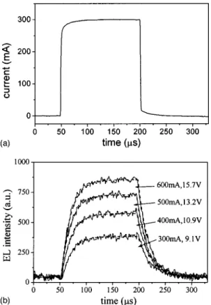
The temporal response of EL from the MOS tunneling diode under the injection of a square-wave current pulse was measured using scanning-gate integrator and boxcar averager system.8Figure 3共a兲 is the waveform of the injection current with 150s duration and Fig. 3共b兲 is the measured temporal EL waveforms from the Al/SiO2/n-Si MOS tunneling diode at a set of injection currents. These measured EL waveforms in the time domain should track the variation of the excess minority carrier density with time.4 Therefore, the minority carrier lifetime near the Si/SiO2 interface can be determined from either the rising-edge or the falling-edge of EL wave-form in the time domain. The rising and falling edges of the temporal EL waveforms are fitted using the following ex-pression:
FIG. 1. Schematic band diagram of the MOS tunneling diode.
FIG. 2. Room-temperature EL spectra from ITO/33 Å SiO2/n-Si tunneling
L共t兲⫽L共⬁兲⫺关L共⬁兲⫺L共0兲兴•exp
冉
⫺ t
冊
, 共1兲where L(⬁) and L(0) denote the final and initial values of the light intensities, respectively, andis the minority carrier lifetime. The minority carrier lifetime is related to the car-rier recombination coefficients A, B, and C through the fol-lowing expression:4
1
⫽A⫹B•N⫹C•N2, 共2兲
where A is the coefficient of Shockley–Read–Hall 共SRH兲 nonradiative recombination through the intraband states near the Si/SiO2 interface, B and C, respectively, are the band-to-band radiative recombination and Auger recombination coef-ficients, and N is the majority carrier density. Figure 3共b兲 shows a good match between the experimental data and the fitting curves. The carrier recombination rates 1/ extracted from the curve fitting in Fig. 3共b兲 at various injection current densities are shown in Fig. 4.
It is seen that at the rising edge of EL waveform, the recombination rate is independent of the injection current. According to Eq.共2兲, this indicates that the SRH recombina-tion is the dominant carrier recombinarecombina-tion process. On the other hand, the recombination rate increases with the injec-tion current at the falling edges of the EL signal, which means that the effect of radiative and Auger recombination cannot be neglected at the EL falling edge. Using least squared method, it is shown that a parabolic curve can well fit the data points of EL falling edge. In the Appendix, we
show that it is a valid assumption that the majority carrier density N is proportional to the injection current density J, i.e., N⫽kJ, when the applied gate voltage is greater than 7.5 V for an Al/SiO2/n-Si MOS tunneling diode with 30 Å gate oxide. Equation 共2兲 then results in the following parabolic relation between the carrier recombination rate 1/ and the current density J:
1
⫽A⫹B•kJ⫹C•k2J2. 共3兲
Therefore, the data shown in Fig. 4 reveal the relative amounts among the SRH recombination, radiative recombi-nation, and Auger recombination.
The intercept A of the parabolic curve关Eq. 共3兲兴 obtained from the least squares fitting to the data points of EL falling edges in Fig. 4 is the SHR recombination coefficient. The SHR recombination lifetimesSHR(SHR⫽1/A) at the rising and falling edges are determined to be 18.0 and 25.8 s, respectively. It is well known that the Si/SiO2interface states with energies near the Fermi level constitute the most active SRH recombination centers2– 4 and the SRH recombination rate approaches a maximum when the recombination centers are located near the midgap region.4The difference in SHR recombination rates between the rising edge and the falling edge of EL signal could be due to a difference in the posi-tions of Fermi level. As the current is just turned on 共rising edge兲, the MOS tunneling diode is still near the flatband condition and the position of Fermi level is close to the mid-gap. Thus the SRH recombination rate is large and depends less on the carrier density N because there is no large accu-mulation of carriers near the Si/SiO2 interface. However, when the MOS tunneling diode is operated at the accumula-tion region, the Fermi level in the n-type silicon substrate is located near the conduction band edge and its variation with the applied voltage is small. There is little change in the SRH recombination rate. Therefore, the position of Fermi level is far away from the valence band edge at the initial stage of EL falling edge. The value of SRH recombination rate A is reduced and is almost the same at various injection current levels at the EL falling edge. As a result, there is lower SRH recombination rate at the EL falling edge when compared to the rising edge. The near-band-edge Fermi level also results
FIG. 3. 共a兲 The waveform of injection current with duration 150s.共b兲 Temporal EL waveforms under the injection of a square current pulse at various injection currents.
FIG. 4. The carrier recombination rates 1/vs the injected current level at the EL rising and falling edges.
in a very large amount of majority carrier accumulated at the Si/SiO2 interface. This large majority carrier accumulation leads to the increase of the recombination rate with the in-jection current at the EL falling edge, as depicted in Fig. 4. The least square fitting using the parabolic curve to the data points of EL falling edges also reveals the information about the radiative and Auger recombinations. The values of B•k and C•k2 are determined to be 194.6 and 2.4 cm4/A2s, respectively. Thus, the ratio among the components of SRH, radiative, and Auger recombinations is 1:0.196:0.096 at the injection current density of 39 A/cm2. For the falling edge, the SRH recombination is still the most important carrier recombination process, but the contributions from radiative and Auger recombinations cannot be ignored. If the Auger recombination coefficient C of 10⫺31cm6/s for holes in bulk silicon is used,4the value of coefficient B is determined to be 4⫻10⫺14cm3/s. This value is nearly ten times larger than that of bulk silicon.4This large increase in the radiative re-combination coefficient in silicon may possibly be due to the momentum compensation facilitated by the Si/SO2 interface roughness and the localized carriers in the potential well near the Si/SiO2 interface.
9–11
Therefore, the larger value of B coefficient facilitates measurement of the minority carrier lifetime near the Si/SiO2 interface using the temporal EL response. The information related to the quality of Si/SiO2 interface can be further deduced based on the measured mi-nority carrier lifetime to characterize the MOS devices with ultrathin gate oxides.
IV. TEMPERATURE DEPENDENCE OF EL AND PL INTENSITIES
Figure 5 shows the measured temperature dependence of the EL and PL intensities from n-type silicon. Both lumines-cences are seen to be quenched by temperature. However, the data show that the EL intensity of the MOS tunneling diode exhibits weaker temperature dependence, as compared to PL. For EL, the normalized luminescence intensity decreases to about 0.6 when the temperature rises to 300 K. In compari-son, the normalized PL luminescence drops to less than 0.1 as the temperature increases to 300 K. The excess carriers for EL and PL are generated by either tunneling effect or
photo-in the band structure and produce a barrier height E*around the recombination center.12The energy E* is called the ac-tivation energy of nonradiative recombination states. Only the carriers with sufficient energy to overcome this barrier can recombine nonradiatively. Therefore, increasing the tem-perature will enhance the nonradiative recombination and thus quench the luminescence. The usual approach to extract the activation energy E* from the temperature dependence of luminescence intensity is to fit the experimental data by the following theoretical and semiempirical expression:12–15
共T兲⫽1⫹C 1
nrexp共⫺E*/kBT兲
, 共4兲
whereis the luminescence intensity normalized at 0 K, T is the temperature, kB is the Boltzmann constant, and Cnris a constant describing how efficiently the nonradiative recom-bination state reduces the luminescence. An efficient nonra-diative recombination process corresponds to a large value of Cnrand a small value of activation energy E*.
The values of Cnrand E*obtained by curve fitting to the experimental PL and EL data are also shown in Fig. 5. For EL, there is a smaller Cnrvalue 共2.8 vs 13.0 for PL兲 and a larger E* value 共35.0 vs 22.5 meV for PL兲. This indicates that the nonradiative recombination state is less thermally active and less efficient, which results in a greater lumines-cent efficiency for EL at room temperature. For the MOS tunneling diode operated in the accumulation region, the ap-plied gate voltage attracts the majority carriers and causes their confinement in a small potential well near the Si/SiO2 interface. On the other hand, the excess carriers generated by the laser illumination distribute over about one carrier diffu-sion length. Since the PL intensity is known to be very sen-sitive to the nonradiative recombination on the surface,4the nonradiative recombination events in the bulk silicon can be neglected. Therefore, the difference in the nonradiative re-combination rate due to the different Fermi-level positions near the Si/SiO2 interface for EL and PL is the most likely cause for the significant difference in the temperature depen-dence of EL and PL shown in Fig. 5.
V. VOLTAGE-DEPENDENT PL INTENSITY
To further confirm the arguments stated above, voltage-dependent PL intensity was also measured from an ITO/SiO2/ p-Si MOS tunneling diode at room temperature. The transparent ITO electrode allows the transmission of 514.5 nm green line from an Ar⫹ laser for optical pumping
FIG. 5. The dependence of EL and PL intensities on temperature. The squares and circles are the data points of EL and PL experiments, respec-tively. Solid line: theoretical fitting.
and simultaneous application of the bias voltage. Figure 6 shows the variation of PL intensity with the applied gate voltage at different pumping powers. When the MOS tunnel-ing diode was not biased, the measured PL was similar to the case of bulk silicon. However, the luminescence intensity was found to increase no matter when the device was under forward or reversed bias. In Fig. 6, the negative and positive gate voltages correspond, respectively, to the forward and reverse bias of the MOS tunneling diode on p-type silicon substrate. For the devices using the n-type silicon substrate, the measured results of voltage-dependent PL intensity were similar. Because the PL was measured only at the chopped frequency of pumping laser, the measured PL intensity did not contain the possible EL signal. Figure 7 shows the nor-malized PL spectra at the gate voltage of⫺4, 0 and ⫹4 V, respectively. Though the PL intensity increases with the ap-plied gate voltage, Fig. 7 shows that the spectral shapes re-main the same. This means that the carrier radiative recom-bination mechanism is not strongly influenced by the applied gate voltage. The current–voltage (I – V) characteristics of the MOS tunneling diode with and without the optical pump-ing are shown in Fig. 8. At reverse bias, the photogenerated carriers in the silicon substrate diffuse and are swept by the bias electric field to the Si/SiO2 interface, and then tunnel through the oxide to the ITO gate. Therefore, the tunneling
current increases significantly at reverse bias under laser il-lumination. Clearly, an ITO/SiO2/Si structure with the ultra-thin oxide could be utilized as a photodetector.
Several important features are revealed by the measured data shown in Fig. 6. The PL intensity remains low for a small bias voltage between 0 and ⫺0.8 V. In this range of bias voltage, the Fermi level in silicon is near the midgap region and far away from both the conduction and the va-lence edges, leading to less accumulation of carriers at the Si/SiO2 interface. From Eq. 共2兲, a low accumulated carrier density results in a small radiative recombination rate. Also, according to the previous PL study, the PL intensity is very sensitive to the surface recombination.4A carefully prepared surface would reduce the surface recombination and, thus, improve the luminescence efficiency. As mentioned in Sec. III, the most active SRH recombination centers are those Si/SiO2interface states with energies near the Fermi level.2– 4 The most effective SRH recombination centers are those lo-cated near the middle of the band gap.4Therefore, the near-midgap Fermi level also results in a large nonradiative re-combination rate. The reduced radiative rere-combination rate and the enhanced SRH recombination due to the near-midgap Fermi level cause the lower PL efficiency at such a small bias region.
When the forward bias is increased from 0 to⫺4 V, the PL intensity increases drastically. Increased forward bias causes bending of the valence band edge toward the Fermi level in the p-type silicon substrate and results in accumula-tion of majority holes at the Si/SiO2 interface. The large amount of majority holes enhances the radiative recombina-tion rate, and in the mean time the near-band-edge Fermi level reduces the SRH recombination process. Thus, the PL intensity increases with the forward bias voltage. At suffi-ciently large forward bias voltage, the position of Fermi level near the Si/SiO2interface approaches the valence band edge and its variation with the applied voltage is small. This re-sults in a small change for the SRH recombination. Since SRH recombination near the Si/SiO2interface is shown to be the most important carrier recombination process 共see Sec. III兲, the PL intensity eventually saturates under forward bias greater than ⫺4 V, as shown in Fig. 6.
FIG. 6. The dependence of PL intensity on gate bias voltage at various optical pumping power ( P3⬎P2⬎P1).
FIG. 7. The normalized PL spectra under the applied gate voltage⫺4, 0, and⫹4 V, respectively.
FIG. 8. The I – V characteristics of the ITO/33 Å SiO2/ p-Si tunneling diode
Similarly, the PL intensity also increases drastically when the reverse bias is increased from 0 to 3 V. The argu-ment provided above for the increase of PL intensity with forward bias also holds for the case of reverse bias. The Fermi level moves toward the conduction band edge and causes reduction of SRH recombination and accumulation of electrons. As a result, the luminescence is greatly enhanced. When the device is under a reversed bias larger than 3 V, the PL begins to drop. This dependence could be attributed to the strong electric field near the Si/SiO2 interface. Because the silicon surface is inverted and a depletion region is formed under large reversed bias, there exists a strong electric field near the Si/SiO2 interface. The typical value of ionization field for excitons in semiconductors is in the order 104 V/cm.16,17 Therefore, the strong electric field (⬃105 V/cm) resulting from the 3 V reversed bias causes the dissociation of excitons and also sweeps the carriers out of the interface before they recombine.
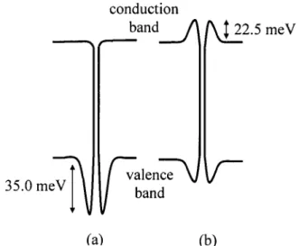
In summary, when the MOS tunneling diode is under either forward or reversed bias, the resulting band bending leads to the near-band-edge Fermi level at the Si/SiO2 inter-face. This results in the reduction of the nonradiative recom-bination through the interface states and also the enhance-ment of the radiative recombination. Since the SRH recombination is the dominant recombination process in the MOS tunneling diode, the variations of PL intensity with bias voltage as shown in Fig. 6 are mainly the result of the change of SRH recombination rate due to the different posi-tion of Fermi level. Therefore, it is concluded that the near-band-edge Fermi level is essential for enhanced lumines-cence no matter whether the carriers are photoexcited or injected through tunneling. In the case of EL from the MOS tunneling diode on n-type silicon substrate, the Fermi level at the Si/SiO2 interface is near the conduction band. The most active SHR recombination centers are efficient electrons traps, but it is difficult for them to capture the minority holes. Hence Fig. 9共a兲 is proposed for the schematic diagram of the nonradiative recombination states for EL. There is a large barrier height for the minority holes. In comparison, in the case of PL without bias voltage, the Fermi level is located
VI. CONCLUSION
EL and PL at the silicon band gap energy from the MOS tunneling diodes on silicon have been studied. The radiative and nonradiative recombinations near the Si/SiO2 interface are characterized by measurement of the temporal EL re-sponse, the temperature dependence of EL and PL intensities, and the voltage-dependent PL intensity. As compared to the bulk silicon, the radiative recombination coefficient in the light-emitting MOS tunneling diode is nearly one order of magnitude larger. The nonradiative SRH recombination is shown to be the dominant interband carrier recombination process. Therefore, the EL efficiency of the MOS tunneling diode can be higher if the amount of the nonradiative recom-bination states near the Si/SiO2 interface is significantly re-duced. The voltage-dependent PL intensity results from the variation of nonradiative recombination rates, which is due to the change of the Fermi level near the Si/SiO2 interface with the bias voltage. The near-band-edge Fermi level for EL results in reduced and less thermally active nonradiative re-combination, as compared to PL. Therefore, the EL intensity is less temperature dependent than PL. This study shows that the location of Fermi level near the Si–SiO2 interface strongly influences the nonradiative SRH recombination rates and, thus, the EL and PL intensities.
APPENDIX
The physical argument for the linear approximation be-tween the injection current density J and the majority carrier density N is discussed as follows. The relation between cur-rent density J and carrier density N is expressed as18
J⫽T•qNv, 共A1兲
where q is electronic charge, is the average drift velocity and T is the tunneling probability across the oxide. The av-erage drift velocity is saturated due to the high electrical field at the Si/SiO2interface.4,19The tunneling probability T is given by the Wentzel–Kramers–Brillouin approximation4
T⬇exp
冉
⫺ CT 共Vox/dox兲冊
, 共A2兲
where Vox is the voltage drop across the oxide, dox is the thickness of the oxide, and CT is a constant. The tunneling
probability T depends on the oxide voltage Vox. The current density for Fowler–Nordheim tunneling JFNand that for di-rect tunneling JDirare derived as follows:4
FIG. 9. Schematic diagram of nonradiative recombination states for the case of共a兲 EL and 共b兲 PL.
JFN⫽AFN
冉
Vox dox冊
2 exp冉
⫺ BFN 共Vox/dox兲冊
for qVox⬎B, 共A3a兲 JDir⫽ AFN 共1⫺冑
1⫺qVox/B兲2冉
Vox dox冊
2 exp冉
⫺ BFN 共Vox/dox兲 ⫻共1⫺冑
1⫺qVox/B兲3/2冊
for qVox⬍B, 共A3b兲 where AFNand BFNare constants andBis the barrier height at the Si/SiO2interface. The values of AFNand BFNare given by4AFN⫽1.57⫻10⫺6A/V2, 共A4a兲
BFN⫽2.57⫻108V/cm2. 共A4b兲
The total applied voltage V across the whole MOS tunneling diode is expressed as
V⫽Vox⫹I•R⫹s⫽Vox⫹AG•J•R⫹s, 共A5兲
where I is the total injection current, R is the resistance of the silicon substrate, and AG⫽0.0154 cm2 is the gate electrode
area. Furthermore, J is the current density given by Eqs. 共A3a兲 or 共A3b兲, depending on either Fowler–Nordheim tun-neling or direct tuntun-neling, S is the surface potential at the
Si/SiO2 interface and is almost a constant when the silicon surface is strongly accumulated. The resistance R is approxi-mated by 15⍀ for the n-type silicon substrate with resistiv-ity of 1–10⍀ cm and 500m thickness. Figure 10 illustrates the relation between the oxide voltage Voxand the total ap-plied voltage V, which is obtained by using Eqs.共A3兲–共A5兲 for dox⫽30 Å. When the total applied voltage V is greater than 7.5 V, the increase of the oxide voltage Vox becomes saturated. The saturation of the oxide voltage Vox is due to the large voltage drop on the silicon substrate at high injec-tion current. According to Eq.共A2兲, the tunneling probability T will approach constant when the total applied voltage is increased beyond 7.5 V. As a result, the expression in Eq. 共A1兲 shows that the current density J is linearly proportional to the carrier density N at high applied voltages.
ACKNOWLEDGMENT
This work was supported by the Academia Sinica, Taiwan.
1
E. J. Lerner, IBM Research, Number 4共1999兲.
2
T. Hori, Gate Dielectrics and MOS ULSIs: Principles, Technologies, and
Applications共Springer, Berlin, 1997兲.
3E. H. Nicollian and J. R. Brews, MOS Physics and Technology共Wiley,
New York, 1982兲.
4
D. K. Schroder, Semiconductor Material and Device Characterization, 2nd ed.共Wiley, New York, 1998兲.
5K. J. Yang and C. Hu, IEEE Trans. Electron Devices 46, 1500共1999兲. 6C. W. Liu, M.-J. Chen, I. C. Lin, M. H. Lee, and C.-F. Lin, Appl. Phys.
Lett. 77, 1111共2000兲.
7
M. J. Chen, E. Z. Liang, S. W. Chang, and C. F. Lin, J. Appl. Phys. 90, 789
共2001兲.
8M. J. Chen, C. F. Lin, M. H. Lee, S. T. Chang, and C. W. Liu, Appl. Phys.
Lett. 79, 2264共2001兲.
9
C. W. Liu, M. H. Lee, M. J. Chen, I. C. Lin, and C. F. Lin, Appl. Phys. Lett. 76, 1516共2000兲.
10C. F. Lin, C. W. Liu, M. J. Chen, M. H. Lee, and I. C. Lin, J. Appl. Phys.
87, 8793共2000兲.
11C. W. Liu, M. H. Lee, M. J. Chen, C.-F. Lin, and M. Y. Chern, IEEE
Electron Device Lett. 21, 601共2000兲.
12J. I. Pankove, Optical Processes in Semiconductors 共Dover, New York,
1971兲.
13E. H. Bogardus and H. B. Bebb, Phys. Rev. 176, 993共1968兲. 14
D. Bimberg, M. Sondergeld, and E. Grobe, Phys. Rev. B 4, 3451共1971兲.
15
W. Ruhle, W. Schmid, R. Meck, N. Stath, J. U. Fischbach, I. Strottner, K. W. Benz, and M. Pilkuhn, Phys. Rev. B 18, 7022共1978兲.
16D. F. Blossey and P. Handler, in Semiconductor and Semimetals, edited by
R. K. Willardson and A. C. Beer,共Academic, New York, 1972兲, Vol. 9, pp. 257–314.
17I. A. Merkulov and V. I. Perel, Phys. Lett. A 45, 83共1973兲. 18J. G. Simmons, J. Appl. Phys. 34, 1793共1963兲.
19S. M. Sze, Physics of Semiconductor Devices, 2nd ed.共Wiley, New York,
1981兲.