Test time reduction for scan-designed circuits by
sl id i ng com pat i b
i I i ty
J.-S. Chang C.-S. Lin
Indexing terms: Logic testing, Scan design, Stuck-atfaults, Test time reduction
Abstract: A postgeneration method for test time
reduction of scan-designed circuits is developed. The maximum overlapping condition between consecutive applied patterns is identified. The application of the condition facilitated with the developed active sliding compatibility process sig- nificantly reduces the number of test clocks. It is demonstrated that the test clocks can be reduced by 50% on average from given test sets. Further evaluation shows that, for parity scan, the test clocks required by the authors’ method are only
41 % of those elsewhere.
1 Introduction
To increase the fault coverage and the test quality of sequential circuits, the now popular scan design had been proposed [13]. The main feature of scan design is that, by scanning the flipflops, the complicated sequential test problem is transformed into the much simpler com- binational one, to achieve the desirable test quality. However, the necessity to shift test patterns and responses in the long scan chain may incur significant increase in test application time as well as test cost. To minimise the additional testing time while retaining test quality of scan design, various scan clock reduction methods have been proposed [l-5,7].
These previous works of test time reduction for scan designed circuits can be divided into the following two general approaches: reduction during test generation or after test generation. To reduce the test application time during test generation, one way is to generate as compact a combinational test set as possible. Several effective techniques have been developed to generate such com- pacted test sets [6, 8, 91. However, as pointed out in Ref- erence 3, test compaction alone is not enough to reduce test application time because further reductions can always be obtained by carefully rearranging the test pat- terns. Alternatively [4, 71, the test generation is made to switch between scan mode and nonscan mode, and the scan mode is used only to achieve the required fault coverage. However, for circuits with many sequential hard-to-be-detected faults, scan operations will occur fre- quently and result in test time worse than that of full scan [4]. Moreover, complicated sequential test gener- ation is involved in the process with the consequence of prolonged generation time.
Q IEE, 1995
Paper 1520E (C2, EIO), received 31st March 1994
The authors are with the Department of Electrical Engineering, Na- tional Taiwan University, Taipei, Taiwan, Republic of China I E E Proc.-Comput. Digit. Tech., Vol. 142, N o . I , January 1995
The postgeneration approach is characterised by reducing scan requirements from a given test set. In Ref- erences 1 and 2, based on the assumption that scan-in and scan-out flipflops are disjoint, each of the scan-in patterns is divided into several segments first. Then, the application of a test pattern to the CUT is invoked after scanning in only a segment but not necessarily a com- plete pattern. Thus some faults originally detected by the later patterns may become detectable by these segmented patterns, and the test time can be reduced due to pattern removal. More elaborate pattern overlapping techniques have also been developed [7]. The overlapping of suc- cessive patterns are obtained by precisely controlling the scan operation through the utilisation of don’t care bits in the scanned flipflops. However, for a given test set with few don’t care bits, the overlapping often collapses owing to the minor difference between successive patterns. In summary, the effectiveness of these previous works is heavily restricted by the characteristics of the given test set.
Recently, a novel idea, parity-scan design, has been proposed [3], in which an extra parity output is intro- duced to the scanned flipflops to enhance the observ- ability. With this simple parity output, the scan operation can be eliminated if the fault effects can be easily observed, and the content of flipflops can be reused. To exploit the enhanced facility, direct test time reduction has been considered [3] by generating a pattern with part of the previous pattern as the constraint so that a test set with highly overlapping patterns can be obtained. As shown in [3], the test time is reduced by 30% on average with the modified FAN [12]. However, the high overlapping among patterns is obtained at the expense of a much larger test set and, as a result, even with the parity output, the reduction in test time is often inferior to that by compacting the test set for pure scan design.
The above observations suggest that, to obtain more consistent good results in test application time reduction, the postgeneration approach with a compact test set is preferable. Given a compact test set for the full scan circuit, the subsequent reduction procedures can then be proceeded based on these information embedded in the test set. One obvious advantage is that the given test set can be served as a bound of test time to ensure the sub- sequent procedures generate even superior results. Another advantage is that the test set provides a global information to guide the priority decision in the reduction procedures. Furthermore, prior to the test time reduction, the test generation flow is the same as that without special consideration on test time reduction. Namely, the decision of performing test time reduction can be made after a test set is obtained. Then test engin- eers can decide whether further reduction on test applica- tion time is necessary. This reduction-on-demand feature 41
is not possible in the reduction during test generation
approach.
We are going to show in this paper that more signifi-
cant reduction of test clocks in scan-designed circuits can
be achieved by the post generation approach. Namely,
the reduction is performed after an initial test set is gen-
erated. We identify the condition which allows the
maximum overlapping between successive applied pat-
terns and then actively modify these patterns to exploit
the overlopping without sacrificing fault coverage. The
experimental results on 22 ISCAS89 benchmark circuits
show that, for the test sets generated by PODEM,
50%
test clocks in pure full-scan can be reduced on average.
Furthermore, for the parity scan design proposed in Ref-
erence 3, our method needs only 52% test clock cycles of
those generated in Reference 3. When the given test set is
already compact, the improvement over Reference 3 is
even more significant, only 41
%test clocks are required.
The reduction is achieved strictly on the domain of com-
binational circuit.
2 Scandesign
For a scan-designed circuit as shown in Fig.
1,each test
pattern
tfor the CUT (circuit under test) consists of two
parts: the part applied to PI denoted as PI(t) and the
DI (t)
4
scan out
Fig. 1 Scan-designed circuit
other part for the FFs (flipflops) as DI(t). In the test
application of
t,DI(t)
must first be shifted into the scan
path which generally consists of all
FFs in the circuit. Let
RESP(t) be the resonse of CUT after applying
t.RESP(t)
can be similarly divided into PO(t) and DO(t), where
PO@)
is the response appearing at PO and DO(t) is that
to be loaded into
FFs. DO(t) must also be shifted out of
the scan path for observation, which may overlap with
the scan-in of the next pattern.
Let T be the test set to be applied and D be the
number
of shifts for each pattern (in general, D is the
number of scanned flipflops), then total testing time
t ,is
t T = ( I T I
+
1)*
D
*
S +IT1
*
C
(1)where S and C are the periods of a shifting clock and
system clock, respectively. Assuming
S =C ,
t ,becomes
t,=((ITI
+
1)*
D + I T I ) *
S (2)The total test clocks of T for a scan-designed circuit
T T C
is then
(3)
T T C
=( I
TI
+
1)*
D
+
IT1
42It can be seen that T T C is dominated by
1
TI
and D.
Therefore, to reduce the total test clocks, we can either
compact the test set T as small as possible or shorten the
number of shifts for each pattern. In Reference 3, the goal
of test generation concentrates on how to increase the
overlapping parts among patterns without giving due
consideration to the test set size. As a result, the test
clocks are not necessarily reduced because test set size
I
T
I
is sacrificed for smaller effective D. Therefore, in our
proposed postgeneration method, test clock reduction
will start from a given set for CUT, preferably a compact
one, then further test clock reduction on effective D can
be carried out. There already exist effective test set com-
paction tools such as COMPACTEST [9] and TSR
[SI.
At present, TSR has been adopted in our work. There-
fore, in this paper, we will aim at how to reduce the
number of test clocks on D.
3 Maximum overlapping
Given a test set, the primary step of test clock reduction
is to identify the maximum overlapping possible between
two consecutive patterns without sacrificing fault cover-
age. In this section, the condition for maximum overlap-
ping will be discussed.
Since the purpose
of reduction is to use the current
content of FFs as part of the next scan-in pattern, two
types of overlapping are possible, either overlapping with
the response of the previous pattern or the previous
pattern itself. Both need some elaboration. In the first
case, one must be sure that the content of
FFs is not
contaminated by the fault effect of all possible faults
under consideration. And, in the second case, the fault
effect should be observed directly from primary outputs
and the
FFs retain the previous pattern by skipping the
load response operation.
Two special cases for pattern overlapping have been
proposed in Reference 3. Under the constraint that all the
activated faults of the current applied pattern
tican be
observed at POs, the following two cases are accepted for
reducing the test clocks of the next pattern
t i + l .Case a:
Complete DO-reuse: DO(ti)
Case b:
Complete DI-reuse: DI(ti)
=
D I ( t i + J
The
‘=’ above is the compatible relation. Two vectors
are said to be compatible if all the corresponding bits are
either of the same logic value or one of them is
‘x’(don’t
care). For example, the two vectors,
01 = (0x01)and
u2
=(OlOx),
are compatible and denoted as
u l
=
u2.
When one of the above two cases is satisfied, the current
content of F F s can be completely reused as part of
t i + land the scan-in operation of tiel can be eliminated.
However, the conditions used in Reference 3 are clearly
restrictive. The general conditions for maximum overlap-
ping will be described next.
To allow maximum overlapping, we will first examine
the conditions by which the content of FFs can be safely
reused. As discussed in the beginning of this Section, to
reuse the DO-part, one must be sure that no fault effect
will appear in
FFs. In other words, the content of FFs
must be the fault-free response to allow safely reuse. This
is by no means trivial since the fault effect of some faults
can only be observed after scanning out the content of
FFs.
Nevertheless, we generally need not scan out the
whole chain to determine whether or not it is the fault-
free response. This is stated in the following observation.
D I ( t i + l )
3.1 Observation I (DO-Reuse)
Under single fault assumption, after applying a pattern t to the CUT and loading its response DO@) into the scanned FFs, the presence of a detectable faultfof t can be determined from either POs or its first fault effect bit in DO(t). Furthermore, if POs and the first fault effect bits of all detectable faults o f t in DO(t) have been observed to be fault free, then these faults are not present and D O ( t ) is the fault-free response.
The above observation can be easily justified. For a given detectable fault of a pattern t, its presence in a circuit can be observed from P O s or DO(t) in which one fault effect bit will be enough. In addition, for all detect- able faults, their presence can also be determined from POs and one fault effect bit in DO(t) for each fault. If any of these faults is determined to be present in a circuit, the circuit is declared faulty and, for testing purpose, no further test application will be needed. Otherwise, none of the detectable faults of t is present and the response DO(t) must be the fault-free response. The single fault assumption ensures that no fault masking effect can occur.
The implication of Observation 1 is that, after examin- ing a few possible fault effect bits in DO(t), the remaining fault-free response may provide an overlapping chance with the next pattern. From the observation, the number of bits to be shifted out after applying a pattern is then MAX(MINBIT(f)) for each detectable fault
f
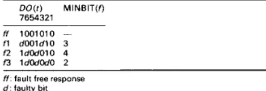
by the pattern. This number can be easily determined by the fault simulation before actual test application. After shift- ing out this predetermined number of bits, it can be decided whether or not the remaining bits are fault-free and can be safely reused. For the example shown in Table 1, suppose three faults {fl,f2,f3} are detected by applying patternr
and the fault-free DO(t) = (1001010),by means of possible fault-effect bits computation in DO(t), the faulty bit nearest to the scan-out pin is selected as MINBIT(f). Since the maximum of MINBIT is found to be 4, DO(t) must be shifted out 4 bits before reusage.
Table 1 : Example of MAX(MINBIT(f)) computation D O ( f ) MINBIT(f) 7654321 ff 1001010 - fl dOOldlO 3 f2 ldOdOlO 4 f3 ldOdOdO 2
ff. fault free response
d : faulty b i t
The Di-reuse condition is the same as described earlier and formally given as follows.
3.2 Observation 2 (DI-reuse)
The current pattern in the F F s , DI(ti), may be part of
D1(ti+J only if all the detected faults of ti can be observed at POs alone.
It can be seen that when fault effects must be observed from FFs, the DI-reuse can not be applied. The problem can be significantly alleviated if extra hardware is used to enhance observability such as that in parity scan designed circuits [3].
The above two observations are the necessary condi- tions to reuse the current content of FFs. The following observation provides a sufficient condition for overlap- ping the next pattern with the current content of FFs, so that the test clocks can be reduced.
I E E Proc.-Comput. Digit. Tech., Vol. 142, No. I , January 1995
3.3 Observation 3 (maximum overlapping)
The current content of FFs, SFF(ti)(DZ(ti) or DO(ti), may constitute part of D I ( t i + without sacrificing fault cover- age if the conditions of Observations 1 or 2 are satisfied and TAIL(SFF(ti) HEAD(DI(t,+ J), where TAIL and HEAD are the trailing and leading parts during scan, respectively.
The last condition of Observation 3 requires only that the trailing part of SFF(ti) is compatible with the leading part of D I ( t i + J without explicitly specifying the size of parts. The condition is named sliding compatibility of S F F ( t , ) and D I ( t i + l ) . Sliding compatibility is the gener- alisation of complete compatibility for test clock reduction.
The extent of overlapping which can be actually achieved from the above observation depends on the ord- ering of scan chain. Although it is theoretically possible to rearrange scan path to obtain maximum reduction, physical constraints discourage such arbitrary rearrange- ment. Hence the aspect of rearrangement is not discussed and, in our experiment, the natural ordering of scan path is used.
Based on Observation 3, the process for maximum overlapping can be performed as follow. In the previous example in Table 1, after shifting four bits out of DO(t) = (lOOlOlO), there are still three bits can be over- lapped with the next pattern. In other words, three scan clocks can be reduced if the next pattern is compatible with (xxxx100). To take fullest advantage of this situ- ation, the next pattern can be chosen accordingly. When this is not possible, the next choice can be the one that is sliding compatible with (xxxx100) (i.e. compatible with
(xxxxxl0) and then with (xxxxxxl)). Note that, with sliding compatibility, the extent of test clock reduction decreases step by step. In the extreme case, not even sliding compatibility is possible, and regular scan oper- ation must be performed. A more effective implementa- tion of this process will be described in the next Section.
4 Active sliding compatibility
The goal of maximum overlapping is to optimally reuse the current content of scanned FFs in the next scan-in operation. However, for a test set lack of sliding compat- ibility between patterns, the reduction on test clock will not be significant. It means that the effectiveness of maximum overlapping could be restricted by the nature of the given test set. Therefore, to further enhance the reuse in maximum overlapping, we propose the process active sliding compatibility, which actively modifies the test set for sliding compatibility and increases the chance of reuse while keeping the overall fault coverage intact.
The basic idea of active sliding compatibility is to take advantage of the overspecification property of the given test set. Given a fault set F and a set of patterns T , the detectable faults of T in F is denoted as DET(T, F). The faults considered in this paper are single stuck-at faults. For the purpose of detecting all the faults in DET(T,
F),
it is usually not necessary to preserve all bits of each pattern in T specified. For example, for a pattern
t = (01 11 1) in T , DET(T, F ) may still keep intact when t is changed to t’ = (Oxlxl). Note that the difference between t and t‘ is only that some specified bits (‘0’ or ‘1’) in t are modified to don’t care (‘x’). In this case, t is said to be overspecified in T and these bits changed from ‘0’ or ‘1’ to ‘x’ are said to be raised. Comparing t with t’, t’ obviously has more chances to be compatible with any arbitrary vector than t. Thus, when trying to reuse the
current contents of
FFs for the scan-in o f t , modifying t
to t‘ would be a better choice.
In active sliding compatibility, for the next pattern to
be scanned in, those sliding incompatible bits with the
current contents of FFs will be modified (raised) to
‘x’for
re-usage. However, during raising these incompatible
bits, it is essential to preserve the overall fault coverage
DET(T,
F).
The following observation allows us to
perform the raising operation while keeping the fault
coverage intact [SI. Define E S S d t ,
F),
the essential faults
oft, as the set of faults in
F
that can only be detected by
r
but not others in T.
4.1 Observation 4Given a fault set F and a test set T of F, for a pattern
t E
T, if t is substituted by t’ such that D E T ( { t ’ } , F)
2E S S d t ,
F),
T
=T
-
{t}+
{t’}has at least the same
amount of fault coverage as T .
The correctness of Observation 4 can be demonstrated
as follows. Note that
DET(T, F)
=DET(T,
F )
-
D E T ( { t } ,
F )
+
E S S A t ,
F)
where ‘-’ and
‘+’
are the set difference and set union,
respectively. Then
DET(T, F )
GDET(T, F )
-
D E T ( { t } ,
F )
+
D E T ( { t ’ } , F )
if DET({t’},
F)
2E S S d t ,
F).
Thus, T
=T
-
{t}
+
{t’}
has at least the same amount of fault coverage as T .
The implication of Observation
4is that active sliding
compatibility can be performed by rasing some bits of t
while monitoring the detectability of E S S A t , F). And, the
detectability of
E S S d t ,
F)
can easily be verified by fault
simulation.
With Observation 4, the brief procedure for maximum
overlapping described at the end of Section 3 can be
refined to the active sliding compatibility process for
achieving more reductions on test clocks. The process is
illustrated by the following example. As shown in Table
2, for a test set T
= {tl,t,, t,},
after applying
t,,active
Table 2: Example of active sliding compatibilityStep DI Contents Operation = D / ( r , ) ? 654321 Initial D / ( r , ) 101000 D/(r,) 010011 D/(r,) 1 1 1 1 1 0 1 D l ( r , ) 101000 D/(r,) x i x o i o D / ( r 3 ) 1x1 1
i o
2 D/(r,) XIOIOO D/(r,) 01 oxxi D/(r,) 11x110 3 D / ( r , ) xxlOl0 D/(r,) 01x01 1 o/(r.) 11 1x1o
-
-
no no bit raising no bit raising no shift out 1 bits-
bit raising no bit raising no shift out 2 bits -
bit raising no bit raisina yes
-
-- -
sliding compatibility is performed to select the next
applied pattern. Only DI-reuse is considered in this
example for simplicity. Initially, DI(t,), DI(t,) and
DI(t,)are mutually incompatible. In Step
1,after the raising
operation on these incompatible bits, the DI parts of the
three patterns are still incompatible. Therefore, one shift
out operation is performed on DI(t,). In Step 2, after the
D I ( t , )
is shifted out
1 bit, active operations for compat-
ibility is performed on DI(t,) and DI(t,) again. Unfor-
tuntely, it also fails. In Step 3, after the content of D I ( t , )
is shifted out one more bit, the DI parts of t , and t ,
become compatible after raising. Thus, 4 scan clocks can
be saved for the scan-in
of
t,.Without these active
44raising operations, only one scan clock (choosing
t 2as
the next pattern) can be reduced in this example.
The detail of the complete algorithm based on the pro-
posed active techniques for maximum overlapping is
shown in Fig. 2. The algorithm consists of the main
routine Active-Clock-Reduction
and the subroutine
maximum-overlapping(
).In Active-Clock-Reduction( ),
first, the test pattern
twith maximum fault coverage is
chosen as the first applied pattern.
Then, to select the next pattern of the current applied
pattern t, the number of preshifts o f t is obtained by com-
puting the maximum fault-effect bit, MAX-MINBIT(t).
Then, the maximum saved clocks by DO-reuse and the
corresponding next pattern are obtained by calling
maximum-overlapping(
).If the number of preshift is
zero, the reuse of
D I ( t )becomes possible, and the saved
clocks are also computed to compare with that of
DO-
reuse. The one with more saved clocks by DI-reuse and
DO-reuse is then chosen as the test scheme of
t.The
process is continued until the given test set T is empty. In
the subroutine, maximum-overlapping(
),the successive
pattern
t‘of the current applied pattern t is obtained
from the remaining patterns
of T with the most saved
clocks. The searching process is performed in a greedy
way. To find the next pattern t’, each time reuse-vector
DI(t)
or DO(t) is shifted out one bit and all remaining
patterns in T are tried to make compatible with
reuse-vector
by
raising
operations.
If
found,
maximum-overlapping()
terminates. Otherwise, the
reuse-vector is shifted out one more bit and the above
make-compatible process is repeated. The process con-
tinues until all bits of reuse-vector have been shifted out.
If no clock reduction is possible, the one with the largest
fault coverage among the remaining patterns in T will be
chosen as the next pattern.
5 Experimental results
To show the effectiveness of our method (ACT), these test
clock reduction techniques proposed in this paper have
been implemented on SUN4-SPARC2 workstation and
22 ISCAS’89 benchmark circuits are evaluated. In Table
3, the statistics of these circuits are shown, including the
number of primary inputs (PI), primary output (PO),
scanned flipflops (SFF), gates (GATE) and the sequential
fault coverage [I
11
(SEQ-FC%). In addition, two initial
test sets of these circuits are evaluated for both full scan
and parity scan version. One initial test set is generated
by a simple PODEM-like ATPG and the other is its
highly compacted set by TSR [SI. These two test sets can
be regarded as two extremes for an arbitrarily given test
set. The sizes of these four different test sets, two for full
scan and two for parity-scan [3], are also included in
Table 3. For the test sets in PDM-P and TSR-P columns,
they are generated in a similar way to PDM and TSR
test sets except a parity checking path for pseudo POs
(i.e. scanned FFs) and an extra PARITY output are
added during test generation. In Tables 4 and
5,the test
clock reduction results of ACT on the PDM, TSR,
PDM-P, TSR-P test sets are shown. The comparison of
ACT with previous works are provided in Table 6.
In Table 4, the test clocks generated by ACT for
PODEM and TSR test sets are given. The final results
are shown in the ACT column and those only with
sliding but without bit-raising operations are listed in the
SLIDE column. The number after each datum is the nor-
malised ratio with respect to pure full scan (FSCAN) of
the given test set. For the PODEM test sets, by the
I E E Proc.-Comput. Digit. Tech., Vol. 142, No. I , January 1995sliding operation (SLIDE), 29% test clock reduction can be achieved on average as shown in the last row. It can be seen that SLIDE is more effective for those circuits with less scanned flipflops such as s820, s832, s1488 and
When comparing the total test clocks of FSCAN for TSR test sets with those for PODEM test sets in the C/AVG row, less than 1/3 (38268/118036) of the test clocks are required, a very significant reduction on test clocks and
/*
T : the given test set applied t o CUT, F: the fault list of CUT*/
/*
next-t: global variable to store the next scan-in pattern*/
Active_ClockReduction() {
choose a pattern t with m a x i m u m fault coverage f r o m T ; while ( T i s not e m p t y ) {
T = T - { t } ;
preshift-no = M A X M I N B I T ( t ) ; F = F - D E T ( { t } , F ) ;
/*
Compute the saved clocks by DO-reuse*/
DO-save-clk = maximum.overlapping(T, DO(t),pre_shaftho) ; DO-nezt-t = next-t ;
loadresponse = T R U E ; u s e D O = T R U E ;
/*
Try DI-reuse*/
if (preshaft-no == 0) {
/*
D E T ( t , F ) c a n be observed at P O*/
/*
C o m p u t e the saved clocks b y DI-reuse*/
DI-save-clk = maximum-overlapping(T, DI(t),preshift-no) ; D L n e z t - t = next-t ; i f ( D I A a v e - c l k
>
D o s a v e - c l k ) { load-response = F A L S E ; push_test.scheme(t,pre.shift-no, 1oad.response) ; use-DO = F A L S E ; t = DLnezt-t ;1
I
if ( u s e D 0 ) { push-test_scheme(t,pre-shift_no,load.response) ; t = DO-next-t ; J1
1
maximum_overlapping(T, reuse.uector,preshi~_no) { shift-no = pre-shift-no ; while ( s h z f t - n o 5 n u m b e r . o f _ D F F ) { D-content = reuse-vector ; sh?ft_out(D~content,shift-no) ; foreach pattern t' i n T { if (make.compatible(D_content,DI(t'),t') == T R U E ) { nezt-t = t' ; return(no_of_DFF-shift_no) ;1
1
shift..no++ ;1
choose a p a t t e r n t with the m a x i m u m D E T f r o m T a s next-t ; return(0) ;
1
Fig. 2 Algorithm ofactiue sliding compatibility
~ 1 4 9 4 . For those circuits with a large amount of scanned
FFs such as s1494 and s5378, the reduction is less suc-
cessful owing to the difficulty of overlapping between suc- cessive scanned patterns. However, when bit-raising is added to increase the chance of overlapping, as shown in the ACT column, up to 46% and 65% reduction on test clocks for s1423 and s5378 can be obtained, respectively. This shows the effectiveness of the proposed active sliding compatibility process. On average, by ACT, 50% of test clocks for FSCAN can be reduced. For the TSR test sets, although the test sets are much more compact than those of PODEM and hence there is less chance for overlap- ping 27% reduction can still be achieved by our methods. I E E Proc.-Comput. Digit. Tech., Vol. 142, No. I , January 1995
test cost. It demonstrates that using a compact test set as the starting point of test clock reduction is worthwhile, and the efforts on the additional test set compaction can be well justified.
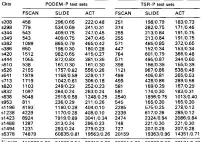
For the parity scan designed circuits, the results of ACT on PODEM-P and TSR-P test sets are shown in Table 5. In comparison with Table 4, with the extra parity output, the average reduction ratio can be increased from 50% to 72% for PODEM test sets and from 27% to 53% for TSR test sets. This shows the posit- ive effect of enhanced observability by the parity output. Note that, for these circuits with more scanned FFs such as s838, s1423 and ~ 5 3 7 8 , the results of ACT on TSR and 45
Table 3: Statistics of ISCAS89 benchmark circuits Ckts PI PO SFF GATE SEQ-FC% PDM TSR PDM-P TSR-P s208 s298 s344 s349 s382 s386 s420 s444 s510 s526 s641 s713 s820 s832 s838 s953 s1196 sl238 sl423 sl488 s1494 s5378 1 1 2 8 3 6 14 9 1 1 15 9 1 1 15 3 6 21 7 7 6 19 2 16 3 6 21 19 7 6 3 6 21 35 24 19 35 23 19 18 19 5 18 19 5 35 2 32 16 23 6 14 14 17 14 14 17 17 5 74 8 19 6 8 19 6 35 49 179 96 119 160 161 158 159 196 181 21 1 193 379 393 289 287 390 395 529 508 657 653 647 2779 63.72 85.71 96.20 95.71 90.98 81.77 41.63 89.45 0.00 75.32 86.30 80.90 81 .88 81.38 29.64 7.78 99.76 94.69 67.39 92.60 92.1 0 74.02 50 51 33 33 50 97 88 47 79 98 88 88 188 180 155 109 222 230 126 176 185 425 27 50 27 25 51 24 14 33 15 14 33 15 25 49 25 63 92 63 44 88 44 25 47 25 57 76 56 50 97 50 24 98 24 24 85 24 96 183 96 97 182 96 76 152 76 76 115 77 124 232 126 133 234 129 32 118 32 104 183 106 102 175 103 109 415 1 1 1 SFF = number of scanned flipflops.
PDM =test size generated by PODEM-like ATPG. TSR =test size of compacting PDM by TSR [6]. PDM-P = test size of PDM with PARITY output. TSR-P = test size of TSR with PARITY output.
*
number of total flipflops.TSR-P test sets are quite close ((1163, 1013), (2285, 2086),
The comparison of ACT with the previous work,
(14252, 14351)). The reason is as follows. Due to a large
parity scan [3], is shown in Table 6. The test clocks by
number of FFs and compacted test sets, the fault effect of
[3] are listed in the PTY-SCAN column. The results of
each fault in these circuits are more likely to reach many
ACT with the parity output are shown in the ACT-
FFs and scan operations for each pattern generally can
PDM(P) and ACT-TSR(P) column, respectively, which
not be avoided. However, from Observation 1, we are
are identical to Table
5.The number after each datum is
able to observe the existence of these faults through a few
the normalised ratio with respect to PTY-SCAN. Com-
shift-out operations almost as effective as adding an extra
paring ACT-PDM(P) and PTY-SCAN, except s1196 and
parity output. It suggests that, in those circuits with large
~1238,
our results are far superior to those of [3]. On
number
of flipflops, it is more advantageous to use the
average, the test clocks of ACT-PDM(P) are only 52% of
proposed ACT starting from the compacted test set, since
those of PTY-SCAN. It shows the effectiveness of the
it can accomplish almost the same amount of test clock
proposed active test clock reduction. In particular, for
reduction as the additional parity chain, albeit without
s1423 and ~ 5 3 7 8 , 61% and 75% reduction can be
any hardware overhead.
achieved, even though the test set size used in [3] are
Table 4: Results of test clock reduction bv ACT
46
Ckts PODEM test sets TSR test sets
FSCAN SLIDE ACT FSCAN SLIDE ACT
s208 458 30110.66 22010.48 251 19810.79 18210.73 s298 779 65410.84 47810.61 389 35410.91 31 710.81 s344 543 47110.87 36010.66 239 22510.94 22410.94 s349 543 47110.87 36010.66 239 22910.96 22710.95 s382 1121 1001 10.89 72810.65 571 53510.94 50410.88 s386 685 41 810.61 40510.59 447 34110.76 34110.76 s420 1512 1 1 1010.73 58210.38 764 63810.84 431 10.56 s444 1055 93710.89 63810.60 571 54510.95 44810.78 s510 559 33310.60 32010.57 405 27310.67 27610.68 s526 2177 1905/0.88 129310.59 1 1 21 103910.93 94710.84 s641 1779 127710.72 64510.36 499 45810.92 37010.74 s713 1779 129310.73 62410.35 499 47510.95 36710.74 s820 1133 680/0.60 63310.56 581 47410.82 47710.82 s832 1085 65710.61 62310.57 587 47910.82 49310.84 s838 5147 366710.71 187210.36 2540 21 01 10.83 1 163/0.46 s953 769 44610.58 42810.56 538 37310.69 37710.70 s1196 4013 161 010.40 72610.1 8 2249 104510.46 57610.26 s1238 4157 155210.37 74510.1 8 241 1 1 1 6110.48 67610.28 s1423 9524 885010.93 51 0910.54 2474 242910.98 2285/0.92 s1488 1238 74710.60 71 110.57 734 58710.80 58710.80 s1494 1301 77010.59 74310.57 720 591/0.82 59110.82 s5378 76679 6979210.91 2653510.35 19799 1961 810.99 1425210.73
CIAVG 1 1 803611 .OO 9894210.71 4477810.50 3862811 .OO 341 6810.83 261 1 1 10.73 FSCAN =test clocks of pure full scan.
SLIDE =ACT without bit-raising. ACT = active sliding compatibility technique.
I E E Proc.-Cornput. Digit. Tech., Vol. 142, No. I , January I995
Table 5: Results of test clock reduction by ACT w i t h PARITY output
Ckts PODEM-P test sets TSR-P test sets
FSCAN SLIDE ACT
FSCAN SLIDE ACT
s208 s298 s344 s349 s382 s386 s420 s444 s510 s526 s641 s713 s820 s832 s838 s953 sl196 sl238 sl423 sl488 Sl494 s5378 458 779 543 543 1099 650 1512 1055 296/0.65 53410.69 409/0.75 40910.75 865/0.79 198/0.30 982/0.65 87210.83 22210.48 241/0.31 24710.45 24710.45 46510.42 41 5/0.27 381 10.36 180/0.28 251 19810.79 28210.75 21 310.84 21 3,084 48510.85 15210.34 601/0.79 49510.87 18310.73 17110.46 19110.75 191,075 37210.65 15310.34 366/0.48 374 255 255 571 447 764 571 398 11 21 499 499 581 581 2540 545 2285 2339 2474 748 727 201 59 34410.60 155/0.39 53810.48 538 21 55 1979 161J0.30 175710.82 1 168/0.59 161/0 30 55610.26 32910.1 7 306/0.18 25210.23 263/0.24 156/0.39 967/0.86 40610.81 26510.53 289/0.58 167/0 29 183/0.31 101 3/0.40 16510.30 27810.12 28510.12 2086/0.84 221 10.30 207/0.28 1435110.71 1719 1103 1097 5048 81 1 41 93 4229 1042/0.61 24910.23 26410.24 291 810.58 428/0.86 169/0.29 174/0.30 189610.75 16510.30 57510.25 61 710.26 1248/0.25 21 1 10.26 40410.10 408/0.10 3041 10.34 296/0.23 279/0.23 1956310.26 23610 29 11 7010.28 1 18010.28 8924 1287 1231 791 9jO.89 31 310.24 29310.24 6083510.81 232410.94 221/0.30 20710.28 74879 1936310.96
71AVG 11 583211 .OO 8407010.54 2971 510.28 3898411 .OO 3030710.62 221 7410.47
FSCAN =test clocks of pure Full Scan. SLIDE = ACT without bit-raising. ACT = active sliding compatibility technique.
Table 6: ComDarison of ACT w i t h P A R I N - S C A N 131 Ckts PTY-SCAN 131 ACT-PDM(P) ACT-TSRIP) Time. s
~ s208 s298 ___ 279 495 461 443 828 380 1296 936 354 1707 ~ 22210.80 241 10.49 24710.54 24710.56 465/0.56 180/0.47 41 5/0.32 38110.41 161 /0.45 55610.33 329/0.57 306/0.42 252/0.52 263/0.56 1248/0.22 21 1/0.09 40411.13 408/1.16 304110.39 296/0.48 27910.40 1956310.25 18310.66 171 /0.35 191 10.41 191 /0.43 372,045 153/0.40 366/0.28 34410.37 155/0.44 53810.32 26510.46 28910.40 2.0 3.0 3.0 3.0 4.0 5.0 7.0 5.0 6.0 s344 s349 s382 s386 s420 s444 s510 s526 $41 s713 sa20 s832 s838 s953* sl196 sl238 sl423 4 4 8 8 sl494 s5378 10.0 12.8 12.1 579 729 487 471 5602 2391 359 351 7894 16710.34 183/0.39 101 310.1 8 20.1 20.7 30.2 16.3 40.1 44.7 60.2 36.8 35.0 1492.0 16510.07 278/0.77 28510.81 208610.26 61 7 702 76739 221/0.36 20710.29 14351/0.19 I / A V G 101 70911 .O 29504/0.52 22009/0.41 -/-
ACT-PDM(P) =results of ACT on PDM-P test sets. ACT-TSR(P) =results of ACT on TSR-P test sets. TIME = CPU time of ACT-PDM(P) on SUN4-SPARCP.
*
=removed from x:/AVG due to different number of scanned FFs.approximately equal to that of the PODEM-P test set
shown in Table 3. The result demonstrates the merit of
the postgeneration approach of test clock reduction. It is
also interesting to compare PTY-SCAN with ACT-
TSR(P). In each evaluated case, the result of ACT-
TSR(P) is far better than that of PTY-SCAN. The
average ratio of test clocks is only
41%.Recall that, in
Reference 3, the test sets are generated by preserving
as
many common parts as possible among patterns to
increase the chance of overlapping. The compactness of
the generated test set is scarified. This comparison result
shows that scarifying the compactness of the test set for
I E E Proc.-Comput. Digit. Tech., Vol. 142, N o . I , January 1995
overlapping is not worthwhile, and a compact test set is
desired for test clock reduction in scanned design.
In the last column of Table 6., the CPU-time for ACT-
PDM(P) is shown. Except ~5378,
all the examples can be
completed in one minute.
For ~5378,
owing to its circuit
size, large test set and scanned FFs, more CPU-time,
albeit not prohibitively long, is required. For ACT-
TSR(P), because the test sets are much more compact
than those of ACT-PDM(P), the CPU-time is far less
than that shown in the Table. For example, in ACT-
TSR(P), the CPU-time for s5378 is only
448seconds.
6 Conclusions
Test time reduction for scan designed circuits has been
investigated in this paper. To reduce the lengthy shifting
operations in the long scan path, post generation method
to optimally reuse the contents of the scanned flipflops
have been developed. Specifically, the condition for
maximum overlapping between successive applied pat-
terns has been identified. This sliding compatibility con-
dition is the generalisation of complete compatibility and
allows more reduction of scan clocks when scanning in
the next pattern. To further enhance the effectiveness of
maximum overlapping, active operations have also pro-
posed to increase the sliding compatibility between suc-
cessive patterns and to maximise the reuse of the FFs’
contents. From the experimental results
on
22 ISCASS9
benchmark circuits, up to
50%test clocks can be reduced
on average by the proposed method. Furthermore, when
the parity output is included in the scan designed CUT,
the resultant test clocks by ACT have been only 41% of
those in Reference 3.
It has been reported that by switching between scan
mode and nonscan mode, further reduction
on test clock
cycles are possible in pure scan designed circuits.
However, a sequential circuit test generation will then be
required, and the test generation time will be substan-
tially increased. To retain the advantage of simple com-
binational test generation of scan designed circuits, the
mode-switching is not performed in this work.
7 References
1 ABADIR, M.S., and BREUER, M.A.: ‘Scan path with look ahead shifting (SPLASH)’. Proceedings of 1986 international test con- ference, pp. 696-704
48
2 ABADIR, M.S.: ‘Efficient scan path testing using sliding panty response compaction’. Proceedings of 1987 international test con- ference, pp. 332-335
3 FUJIWARA, H., and YAMAMOTO, A.: ‘Parity-scan design to reduce the cost of test application’, I E E E Tram., 1993, CAD-12, (lo), pp. 1604-1611
cation time in full scan designs’. Proceedings of 1992 ICCAD, pp.
17-20
5 POMERANZ, I., and REDDY, S.M.: ‘A test application scheme for embedded full-scan circuits to reduce testing costs’. Proceedings of first Asian test symposium, 1992, pp. 206-221
6 CHANG, J.S., and LIN, C.S.: Test set compaction for com- binational circuits’. Proceedings of first Asian test symposium, 1992, pp. 20-25
7 LAI, W.C., KUNG, C.P., and LIN, C.S.: ‘Test time reduction in scan design circuits’. Proceedings of 1993 EDAC, pp. 489-498 8 TROMP, G.-J.: ‘Minimal test sets for conmbinational circuits’. Pro-
ceedings of 1991 international test conference, 1991, pp. 204-209
9 POMERANZ, I., REDDY, L.N., and REDDY, S.M.: ‘COM- PACTEST: a method to generate compact test Sets for com- binational circuits’. Proceedings of 1991 international test conference, pp. 194-203
10 GOEL, P.: ‘An implicit enumeration algorithm to generate tests for combinational logic circuits’, I E E E Trans., 1981, C-30, (3). pp. 215-
222
1 1 CHENG, W.T., and DAVIDSON, S.: ’Sequential circuit test gener- ator (STG) benchmark results’. Proceedings of international symp. of circuits and systems, 1989, pp. 1931-1941
12 FUJIWARA, H., and SHIMONO, T.: ‘On the acceleration of test generation algorithms’, I E E E Trans., 1983, C-32, (12), pp. 1137-
1144
13 EINCHELBERGER, E.B., and WILLIAMS, T.W.: ‘A logic design structure for LSI testability’. Proceedings of design automation con- ference, 1977, pp. 462-468
4 LEE, S.Y., and SALUJA, K.K.: ‘An algorithm to reduce test appli-