國 立 交 通 大 學
電 信 工 程 學 系 碩 士 班
碩 士 論 文
應用於無線通訊系統之電子式可調帶通濾波器
The Electrically Tunable Band-pass Filter with Compact Size and
High Selectivity for Wireless Communication
研 究 生:黃正宏
指導教授:彭松村 博士
黃瑞彬 博士
The Electrically Tunable Band-pass Filter with Compact Size and
High Selectivity for Wireless Communication
研 究 生:黃正宏 Student: Cheng-Hung Huang 指導教授:彭松村 博士 Advisor: Dr. Song-Tsuen Peng 黃瑞彬 博士 Dr. Ruey-Bing Hwang
國 立 交 通 大 學 電 信 工 程 學 系 碩 士 班
碩 士 論 文
A Thesis
Submitted to Department of Communication Engineering College of Electrical Engineering and Computer Science
National Chiao Tung University In partial Fulfillment of the Requirements
for the Degree of Master of Science
in
Electrical Engineering July 2004
Hsinchu, Taiwan, Republic of China 中 華 民 國 九 十 三 年 七 月
應用於無線通訊系統之電子式可調帶通濾波器
研 究 生:黃正宏 指導教授:彭松村 博士 黃瑞彬 博士 國立交通大學電信工程學系碩士班 中文摘要 在這篇論文中,我們發展了一個電子式可調帶通濾波器,這濾波器由開迴路環形共 振器和 varactor 所構成。我們經由電路模擬來計算帶通濾波器的介入和反射損失,此外, 我們也完成了實驗,且由模擬和量測相近的結果,我們更可確定電路模型的正確性。另 外,在共振器上的 varactor 是用來調整共振器的共振頻率,如預期的,由 varactor 所造 成的電抗確實的影響到共振器的總電感和電容值,值得一提的是,不僅濾波器的中心頻 率可以被改變,這電抗是電感性或是電容性也將決定濾波器的中心頻率將大於或小於未 加 varactor 時濾波器的中心頻率,利用這個結果,我們也實現了一個寬的可調頻率帶通 濾波器,雖然不理想之二極體的 Q 值增加了濾波器的介入損失,但這原理是被證明可有 效的用於調變帶通濾波器的中心頻率。The Electrically Tunable Band-pass Filter with Compact Size and
High Selectivity for Wireless Communication
Student: Cheng-Hung Huang Advisor: Dr. Song-Tsuen Peng
Dr. Ruey Bing Hwang
Department of Communication Engineering
National Chiao-Tung University
Abstract
In this thesis, we developed an electrically tunable band-pass filter. The filter contains
multiple sections of open-loop ring resonators and varactors. For the band-pass filter, the
scattering parameters, including the insertion and return losses, has been calculated by means
of electric circuit simulation. In addition, we have also carried out the experimental studies.
The excellent agreements between simulated and measured results prove the accuracy of the
established circuit model. Moreover, the varactor was added to the resonator to adjust its
resonant frequency. As expected, the reactance introduced by the varactor indeed affects the
net inductance and capacitance obviously. It is noted that, not only the shift with the center
frequency, the inductive or capacitive of the reactance can also provide a parameter to switch
its frequency toward the two directions away from the one without varactor. As a consequence,
a wideband tunable band-pass filter is achieved. Although the bad quality factor with the
diode strongly increases the insertion loss, this concept was proved to be available for
誌謝
我要感謝我的指導教授彭松村 教授、黃瑞彬 教授和實驗室同伴們,感謝他們的教 導與幫忙,這篇論文才可以順利的完成,另外我們要感謝我的家人們,感謝他們長期對 我的支持與鼓勵,最後,謹將此篇論文獻給我的父母,感謝他們多年來的辛苦栽培。
Acknowledgement
I would like to thank my advisors Professor Song-Tsuen Peng, Professor Ruey Bing Hwang
and my partners of the lab. It was thanks to their instruction and help that this thesis can be
accomplished successfully. Furthermore, I wish to thank my family for that they have
supported and encouraged me for a long time. In the final, I would like to donate this thesis to
CONTENTS
CHINESE ABSTRACT ... Ⅰ ENGLISH ABSTRACT ...Ⅱ ACKNOWLEDGMENT ...Ⅲ CONTENTS ...Ⅳ LIST OF FIGURES AND TABLES ... Ⅵ
CHAPTER 1
INTRODUCTION ... 1
CHAPTER2 THE BASIC CONCEPT FOR RF/MICROWAVE BAND-PASS FILTER... 3
2.1LOW-PASS PROTOTYPE FILTERS AND ELEMENTS... 4
2.2BAND-PASS PROTOTYPE FILTERS AND ELEMENTS... 6
2.3BAND-PASS FILTERS WITH ADMITTANCE INVERTERS... 7
CHAPTER3 THE EXTERNAL QUALITY FACTOR DESIGN CURVES AND COUPLING COEFFICIENT DESIGN CURVES... 11
3.1THE OPEN-LOOP RING RESONATOR... 11
3.2QUALITY FACTOR DESIGN CURVES... 14
3.3 COUPLING COEFFICIENT DESIGN CURVES... 18
3.3.1 electric coupling and magnetic coupling structures ... 19
3.3.2 electric coupling design curves... 20
3.3.3 magnetic coupling coefficient design curves... 24
CHAPTER4 PRACTICAL REALIZATION OF THE BAND-PASS FILTER FOR MICROSTRIP... 28
CHAPTER5
THE DESIGN METHOD AND PRACTICAL REALIZATION OF THE NEW
TUNABLE BAND-PASS FILTERS ... 37
5.1 THE MECHANISM OF FREQUENCY TUNING... 37
5.2THE TUNABLE BAND-PASS FILTER USING CAPACITANCE REACTANCE X ... 40
5.3THE TUNABLE BAND-PASS FILTER USING INDUCTANCE REACTANCE X... 46
5.4THE BAND-PASS FILTER HAVING WIDE TUNABLE BANDWIDTH... 49
CHAPTER6 CONCLUSION ... 53
REFERENCE ... 54
APPENDIX A ELEMENT VALUES FOR BUTTERWORTH LOW-PASS FILTER ROTOTYPES (G0=1, ΩC=1, LAR=3.01DB AT ΩC=1, N=1 TO 10) ... 56
List of Figures and Tables
FIGURE 2.1 THE LADDER CIRCUITS FOR LOW-PASS FILTER PROTOTYPES AND THEIR ELEMENT
DEFINITIONS ... 3
FIGURE 2.2 THE LADDER LC LUMP CIRCUITS FOR LOW-PASS FILTER PROTOTYPES AND THEIR LUMP VALUE DEFINITIONS... 5
FIGURE 2.3 THE LADDER LC LUMP CIRCUITS FOR BAND-PASS FILTER PROTOTYPES AND THEIR LUMP VALUE DEFINITIONS... 6
FIGURE 2.4 BAND-PASS FILTERS USING ADMITTANCE INVERTERS ... 7
FIGURE 2.5 ADMITTANCE INVERTERS USED TO CONVERT A SERIES INDUCTANCE INTO AN EQUIVALENT ... 8
FIGURE 3.1 A PARALLEL GLC RESONANT CIRCUIT ... 12
FIGURE 3.2 A HALF-WAVELENGTH OPEN-LOOP MICROSTRIP RING RESONATOR ... 13
FIGURE 3.3 A HALF-WAVELENGTH OPEN-LOOP MICROSTRIP RING RESONATOR THAT CONSIDERS EFFECT OF THE GAP... 13
FIGURE 3.4 THE CIRCUIT RESPONSES OF IMPEDANCE MAGNITUDE VERSUS FREQUENCY FOR FIGURE 3.1 A PARALLEL GLC RESONANT CIRCUIT ... 15
FIGURE 3.5 THE RESONANCE CIRCUIT THAT IS COUPLED TO THE SOURCE RESISTANCE RS. ... 15
FIGURE 3.6 PHASE RESPONSE OF S11 FOR THE CIRCUIT IN FIGURE 3.5... 17
FIGURE 3.7 A HALF-WAVELENGTH OPEN-LOOP RING RESONATOR WITH A FEED LINE... 17
FIGURE 3.8 THE DESIGN CURVES OF QE FOR AN OPEN-LOOP RING MICROSTRIP BAND-PASS FILTER OBTAINED BY CIRCUIT SIMULATION ... 18
FIGURE 3.9 TYPICAL COUPLING STRUCTURES OF COUPLED MICROSTRIP SQUARE OPEN-LOOP RESONATORS (A) ELECTRIC COUPLING STRUCTURE. (B) MAGNETIC COUPLING STRUCTURE. .. 19
FIGURE3.10 (A) AN EQUIVALENT LUMPED-ELEMENT CIRCUIT OF ELECTRIC COUPLING STRUCTURE (B) AN ALTERNATIVE FORM OF THE EQUIVALENT CIRCUIT WITH AN ADMITTANCE INVERTER ... 21
FIGURE3.11 THE S21 RESPONSES FOR THE ELECTRIC STRUCTURE WHEN THE COUPLED RESONATOR CIRCUITS ARE OVER-COUPLED ... 23
STRUCTURE... 23
FIGURE3.13 (A) AN EQUIVALENT LUMPED-ELEMENT CIRCUIT OF MAGNETIC COUPLING
STRUCTURE (B) AN ALTERNATIVE FORM OF THE EQUIVALENT CIRCUIT WITH AN IMPEDANCE INVERTER ... 25
FIGURE 3.14 THE S21 RESPONSES FOR THE MAGNETIC COUPLING STRUCTURE WHEN THE
COUPLED RESONATOR CIRCUITS ARE OVER-COUPLED ... 26
FIGURE 3.15 THE COUPLING COEFFICIENT CURVE FOR THE MAGNETIC COUPLED RESONATOR
STRUCTURE... 27
FIGURE 4.1 THE OPEN-LOOP RING BAND-PASS FILTER WITH THE SYMMETRIC FEED LINES... 29 FIGURE4.2 THE S21 OF SIMULATION AND MEASUREMENT FOR THE OPEN-LOOP RING
BAND-PASS FILTER WITH THE SYMMETRIC FEED LINES ... 29
FIGURE4.3 THE S11 OF SIMULATION AND MEASUREMENT FOR THE OPEN-LOOP RING
BAND-PASS FILTER WITH THE SYMMETRIC FEED LINES ... 30
FIGURE 4.4 THE FILTER USING TWO HAIRPIN RESONATORS WITH ASYMMETRIC TAPPING FEED
LINES ... 31
FIGURE 4.5 THE OPEN-LOOP RING BAND-PASS FILTER WITH THE ASYMMETRIC FEED LINES .... 33 FIGURE4.6 THE S21 OF SIMULATION AND MEASUREMENT FOR THE OPEN-LOOP RING
BAND-PASS FILTER WITH THE ASYMMETRIC FEED LINES... 33
FIGURE4.7 THE S11 OF SIMULATION AND MEASUREMENT FOR THE OPEN-LOOP RING
BAND-PASS FILTER WITH THE ASYMMETRIC FEED LINES... 34
FIGURE 4.8 THE S21 OF MEASUREMENT FOR THE OPEN-LOOP RING BAND-PASS FILTER WITH
THE SYMMETRIC AND ASYMMETRIC FEED LINES... 34
FIGURE4.9 THE LAYOUT OF THE FILTER USING FOUR CASCADED OPEN-LOOP RING
RESONATORS WITH THE ASYMMETRIC FEED LINES. ... 35
FIGURE4.10 THE MEASURED RESULTS OF THE FILTER USING FOUR CASCADED OPEN-LOOP
RING RESONATORS WITH ASYMMETRIC FEED LINES. ... 36
FIGURE 5.1 THE CONVENTIONAL STRUCTURE FOR THE ELECTRICALLY TUNABLE FREQUENCY
RESONATOR ... 39
FIGURE 5.2 THE EQUIVALENT CIRCUIT FOR THE VARACTOR CONNECT THE VIA HOLE GROUND
(A) CONSIDERING THE PARASITIC EFFECTS OF THE PACKAGE (B) NEGLECTING THE
PARAMETER CP AND RS... 39
FIGURE5.3 THE NEW STRUCTURE FOR THE ELECTRICALLY TUNABLE FREQUENCY RESONATOR ... 40
FIGURE 5.4 THE MEASUREMENT CIRCUIT FOR LT... 40
FIGURE 5.5 THE SIMULATED RESPONSES FOR CT AND X VERSUS F0... 41
FIGURE 5.7 THE LAYOUT OF THE NEW TUNABLE BAND-PASS FILTER ... 42 FIGURE 5.8 THE SIMULATION OF THE TUNABLE BAND-PASS FILTER WITH THE CAPACITANCE
REACTANCE X AND THE BW= 50MHZ ... 43
FIGURE5.9 THE MEASUREMENT OF THE TUNABLE BAND-PASS FILTER WITH THE CAPACITANCE
REACTANCE X AND THE BW= 50MHZ ... 43
FIGURE5.10 THE MEASUREMENT OF THE TUNABLE BAND-PASS FILTER WITH THE
CAPACITANCE REACTANCE X AND THE BW= 100MHZ... 44
FIGURE 5.11 THE RESPONSE CURVES FOR THE D1 AGAINST THE RESONANT FREQUENCY... 46
FIGURE 5.12 THE SIMULATION OF THE TUNABLE BAND-PASS FILTER WITH THE INDUCTANCE
REACTANCE X ... 47
FIGURE5.13 THE MEASUREMENT OF THE TUNABLE BAND-PASS FILTER WITH THE INDUCTANCE
REACTANCE X ... 48
FIGURE 5.14 THE CIRCUIT OF THE WIDE TUNABLE BAND-PASS FILTER WITH N SWITCHES OF
EACH BRANCH OF THE RING ... 50
FIGURE5.15 THE SIMULATION OF THE WIDE TUNABLE BAND-PASS FILTER FOR ONE SWITCH OF
EACH BRANCH OF THE RING ... 51
FIGURE 5.16 THE MEASUREMENT OF THE WIDE TUNABLE BAND-PASS FILTER FOR ONE SWITCH
OF EACH BRANCH OF THE RING ... 51
TABLE5-1 THE SIMULATION AND MEASUREMENT RESULTS OF THE TUNABLE BAND-PASS
FILTER WITH THE CAPACITANCE REACTANCE ... 45
TABLE5-2 THE SIMULATION AND MEASUREMENT RESULTS OF THE TUNABLE BAND-PASS
FILTER WITH THE INDUCTANCE REACTANCE... 48
TABLE5-1 THE SIMULATION AND MEASUREMENT RESULTS OF THE TUNABLE BAND-PASS
Chapter 1
Introduction
The characteristics of high selectivity, compact size and tunable frequency for modern microwave and millimeter wave filters are highly required for the next generation mobile and satellite communication systems. However, a band-pass filter having these characteristics together in the realization is not easy to achieve. In this work, the design and realization of the tunable band-pass filter with high selectivity, small size and tunable frequency will be presented.
The design methodology of a LC lumped-element filter with butterworth response has been popularly employed. However, two problems arise at microwave frequencies. First, lumped elements such as inductors and capacitors are, in general, available only for a limited range of values and are difficult to implement at microwave frequencies, thus the distributed components are needed to obtain more precise circuit model. In addition, at microwave frequencies the distances between filter components are considerable. Thus, in this thesis, we introduce a filter design methodology using microstrip-line resonator and coupled transmission-line [1].
Using the cross-coupled plannar microwave filters have a characteristic of high selectivity [2], but the they often need at least four resonators and show a high insertion loss [3][4]. Recently, the method of increasing selectivity for filter, however, without increasing its size was proposed by [5]. This method employ the asymmetric feed to produce two transmission zeros in its response. Moreover, since the two zeros locate at the two pass-band edges, it could further enhance the selectivity of the filter. In chapter 4, we verify the method described previously by using numerical simulation and experimental studies both.
In addition, a reconfigurable scheme is incorporated with such a high selectivity and small size filter to achieve purpose of tunable filter design.
Most tunable filters described in the literature are classified into three categories: mechanically tunable, magnetically tunable, and electronically tunable filters [6]. However electronically tunable filters have the characteristics of high-speed tuning over a wide tuning range, and are compact in their size, such as, GaAs varactor diodes [7][8], MESFETs [9] or PET. Although some conventional electrically tunable filters having the advantage of high-speed tuning and small size were reported [10][11], in chapter5 we will propose some new schemes of tunable filters which have small size and wide tunable frequency range and a higher selectivity based on asymmetric feed lines. Beside, by tapping the position of the varactor or switch, the filters have another advantage, that it can compensate that the values of CT and LT to achieve the impedance match. As a result, it provides many possibilities in
choosing the devices.
In chapter 4 and chapter 5, the some simulations and measurements of the filters are presented. In the numerical simulation, we use Microwave Office softwareTM, HP 8722D
network analyzer for measuring the return- and insertion-losses of the filters.
Chapter 2
The basic concept for RF/microwave band-pass filter
This chapter describes some basic concepts for the design of general RF/microwave band-pass filters. The topics to be cover of include: low-pass prototype filters and elements, band-pass prototype filters and elements, and band-pass filters with admittance inverters.
2.1 Low-pass prototype filters and elements
The prototype by a low-pass filter is, in general, defined that whose element values are normalized, such that the source resistance or conductance is equal to unity ( ), and so is the cutoff angular frequency (
1 0 =
g
1 =
Ω ). Figure 2.1 depicts a ladder network for use as a low-pass filter with their elements attached [12]. Here, and are defined as the source and load resistance, respectively, and the g
c
0
g gn+1
i, for i = 1 to n, stand for the series inductors
or shunt capacitors, where n is the number of reactive elements.
g1
g2
g3
g4 gn+1
g0
Figure 2.1 The ladder circuits for low-pass filter prototypes and their element definitions
In the procedures for filter design for the Butterworth low-pass prototype with insertion loss LAr=3.01dB at the unit cutoff angular frequency Ωc =1, the values of elements in figure 2.1
1 0= g (2 . 1) − = n i gi 2 ) 1 2 ( sin 2 π ,for i=1,2,3,……n (2 . 2) 1 1= + n g (2 . 3) , Furthermore, for convenient references, Appendix A gives some typical element values for such filters having n = 1 to10. It is noted that a modified Butterworth response such as Chebyshev response may also be used to design a low-pass prototype filter as that in Figure 2.1 [13].
In the prototype design, not only the element values ( ) are normalized to the source resistance R
i
g
0, but also the frequency Ω is normalized to byω . In order to obtain the actual
frequency response and element values for practical filters based on the low-pass prototype, the impedance and frequency transformations are needed; they are given by:
0 S S R G 1 R = = (2 . 4) 0 i i g R
L = , for g representing the inductance (2 . 5)
0 i i
R g
C = , for g representing the capacitance (2 . 6)
0 1 n L L g R G 1 R = = + (2 . 7)
For the low-pass filter of the cutoff frequencyωc, the frequency transformation is
c
ω
ω =Ω (2 . 8) where RS (GS) and RL (GL) are the source impedance (admittance) and the load impedance
(admittance), respectively. ωc is the cutoff angular frequency of the filter. Combining impedance transforms (2.4) to (2.7) together with frequency transforms (2.8) [13], the element transformations can be written as
c i 0 c i ' i g R L L ω ω =
= , forgirepresenting the inductance (2 . 9)
c 0 i c i ' i R g C C ω ω =
= , forgirepresenting the capacitance (2 . 10) Invoking (2.4), (2.7), (2.9) and (2.10) into the elements in Figure 2.1 can be transformed into those in Figure 2.2. Thus, the Butterworth low-pass filter consisting of LC lump elements can be so designed without any difficulty.
0 0 S g R R = RL =gn+1R0 c
ω
0 1 ' 1 g R L = cω
3 0 ' 3 g R L = 2 0 2 ' 2 R g Cω
= 4 0 4 ' 4 R g C ω =Figure 2.2 The ladder LC lump circuits for low-pass filter prototypes and their lump value definitions
2.2 Band-pass prototype filters and elements
The design of band-pass filters that is a similar design rule of low-pass filters can also use the impedance and frequency transformations described previously. The impedance transformations of the band-pass filter are equivalent to the low-pass filter such as (2.4 ~ 2.7), but the frequency transformation of the band-pass filter is different from the low-pass filter [13]. It is FBW 1 0 0 − = Ω ω ω ω ω (2 . 11) 2 1 0 0 1 2 ; FBW ω ωω ω ω ω = − = (2 . 12)
Here FBW is the fractional bandwidth, ω0 is the center angular frequency of pass band,ω1, 2
ω denote the edges of the passband. When this frequency transformation is applied to reactive element g of the low-pass prototype, an inductive/capacitive element g in the low-pass prototype will transform to a series/parallel LC resonant circuit in the band-pass filter. In [13], the element transformations for the series and parallel resonator in the band-pass filter are written below
i 0 0 ' i FBW R g 1 L =
ω for gi presenting the inductance and Ωc =1 (2 . 13)
i 0 0 ' i 2 0 ' i R g 1 FBW L 1 C = = ω
ω for gi presenting the inductance and Ωc =1 (2 . 14)
0 i 0 ' i R g FBW 1 C =
ω for gi presenting the capacitance and Ωc =1 (2 . 15)
i 0 0 ' i 2 0 ' i g R FBW C 1 L = = ω
ω for gi presenting the capacitance and Ωc =1 (2 . 16)
1 0 0 ' 1 FBW R g 1 L = ω 0 3 0 ' 3 FBW R g 1 L = ω ' 1 2 0 ' 1 L ω 1 C = 0 2 0 ' 2 R g FBW 1 C = ω ' 2 2 0 ' 2 C 1 L ω = ' 3 2 0 ' 3 L 1 C ω = ' 4 2 0 ' 4 C 1 L ω = 0 4 0 ' 4 FBW 1 C R g = ω 0 0 s g R R = RL =gn+1R0 Yin
Figure 2.3 The ladder LC lump circuits for band-pass filter prototypes and their lump value definitions
Adopting the element transformations from (2 .13) to (2 .16) and impedance transformations (2 .4) and (2 .7), the low-pass filter in Figure 2.1 can be easily transformed into a band-pass
filter indicated in Figure 2.3. The transformation method allows us to transform the prototype filter.
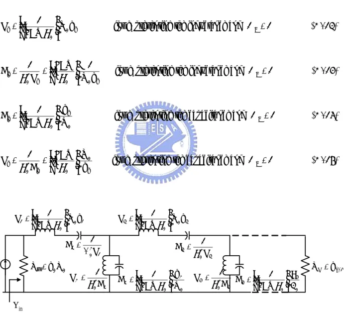
2.3 Band-pass filters with admittance inverters
The band-pass filter structure in Figure 2.3 consists of series resonators alternating with shunt resonators with discrete components, but the arrangement is difficult to implement with planar structures for high frequency applications. In practice, it is much more practical to use a structure which approximates the circuit in Figure 2.4, where the J’s stand for the admittance inverters. An ideal admittance inverter is a two-port network that has a unique property at all frequencies, to transform a shunt-connected element to a series-connected element. Specifically, if the admittance Y2 is connected at one port of the admittance inverters, the
admittance Y1 seen at the other port of the admittance inverters is
2 2 1 Y J Y = (2 . 17) In general, an ideal admittance inverter has the ABCD matrix is given by:
± = 0 jJ jJ 1 0 D C B A m (2 . 18) L2 C2 RL RS J0,1 L1 C1 J1,2 J2,3 Ln Cn Jn,n+1 Yin
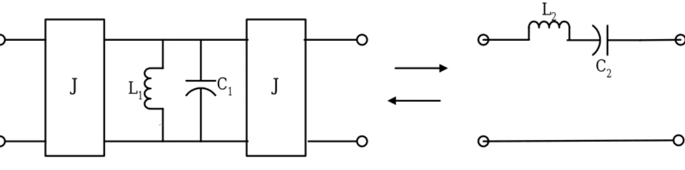
As a simple example to show the function of admittance inverters, a parallel resonator with an admittance inverter on each side is equivalent to a series resonator, as illustrated in Figure 2.5.
J C1 J
L2
L1
`
C2
Figure 2.5 Admittance inverters used to convert a series resonator into an equivalent circuit with parallel resonator
If the parameters in (2.17) and (2.18) are substituted into those in Figure 2.4 and thus Yin in
Figure 2.3 and 2.4 are equivalent, under the condition of Ωc =1, and the admittance-inverter values are 0 1 0 1 0 0,1 R C FBWω J g g = (2 . 19) 1 -n to 1 i , g g C C FBWω J 1 i i 1 i i 0 1 i i, = = + + + (2 . 20) L 1 n n n 0 1 n n, g g R C FBWω J + + = (2 . 21)
In the structure of Figure 2.4, all the resonators are of the same type, so that, the frequency response is the same as that in Figure 2.3. Notice that the structure in Figure 2.4 is more practical than that of Figure2.3 for designing the microwave band-pass filters. Besides, the resonators used in microwave system are generally distributed not lumped, to replace the lumped LC resonators by distributed circuits, such as: distributed circuits can be microwave
cavities, microstrip resonators, or any other suitable resonant structures. We have to make certain the accuracy of the circuit models.
Furthermore, the external Q and the coupling coefficient k are defined as
0 e G B Q = (2 . 22) 1 i i 1 i i, 1 i i 1 i i, 1 i i 1 i i, 1 i i, C C ω J C C C L L L k + + + + + + + = = = (2 . 23)
where, G0 is external load inductance, B is the susceptance of the resonator, Li,i+1 is the mutual
inductance, Li and Li+1 are self inductance, Ci,i+1 is the mutual capacitance, Ci and Ci+1 are self
capacitance [1]. Substituting (2.19) (2.20) (2.21) into (2.22) (2.23), the equation (2.22) (2.23) can be rewritten as below:
FBW g g Q 0 1 1 e = (2 . 24) 1) -(n to 1 i for , g g FBW k 1 i i 1 i i, = = + + (2 . 25) FBW g g Q n n 1 en = + (2 . 26) , (2.24) to (2.26) are generalized equations for designing a band-pass filter only employing shunt-type resonators. The coupling coefficients ki,i+1 is a generalization of the usual
definition of coupling coefficient between the adjacent resonators, the Qe1 is the external
quality factor of the resonators at the input ,and Qen is the external quality factor of the
resonators at the output.
Finally, we list the steps for designing a band-pass filter having merely parallel resonators, given below:
1. Determine the required order n
2. The element values ( ) of a low-pass prototype filter for Butterworth response can be found from equation (2.1) to (2.3) or Appendix A
i
3. Determine the fractional bandwidth FBW and center frequency angular ω0
4. Using equation (2.24) (2.25) and (2.26) to obtain the required parameters of the band-pass filter only adopting parallel resonators.
en 1 i i, e ,k ,Q Q1 +
5. Using distributed circuit to model the resonant circuit in step 4 above.
That practical realization of the band-pass filter in microwave will be discussed in the succeeding chapters.
Chapter 3
The external quality factor design curves and
coupling coefficient design curves
In the preceding chapter we had outlined the steps for designing practical band-pass filters which employ only parallel resonators in microwave. In this chapter we not only verify that a half wavelength open loop of microstrip indeed is a parallel resonator, but also discuss the method for refining the external quality factor design curves and coupling coefficient.
3.1 The open-loop ring resonator
Near resonance, a microwave resonator usually can be modeled by an equivalent circuit series or parallel RLC lumped-elements. Where the resistor (R) is the resonator’s loss and, if the resonator is lossless, the R vanishes. Now, an opened-loop half-wavelength ring microstrip line can be modeled by a parallel RLC lumped-element equivalent circuit, which will be derived as follows.
Figure 3.1 shows a parallel RLC resonant circuit. The input admittance is
L j 1 C j R 1 Yin ω ω + + = (3 . 1)
C
L
R
+
V
-Y
in1
Z
in=
Figure 3.1 A parallel GLC resonant circuit
Now consider the behavior of the input admittance of this resonator near its resonant frequency. Lettingω =ω0 +∆ω, where ω0 is resonant angular frequency and ∆ω is small compared toω0, such that (3.1) can be written to
(
)
(
)
(
)
1 1 L j 1 C j R 1 L j 1 C j R 1 Y 0 0 0 0 0 in ω ω ω ω ω ω ω ω ω ∆ + + ∆ + + = ∆ + + ∆ + + = (3 . 2)by using the result of Maclaurin expansion, thus (3.2) can be rewritten as
(
)
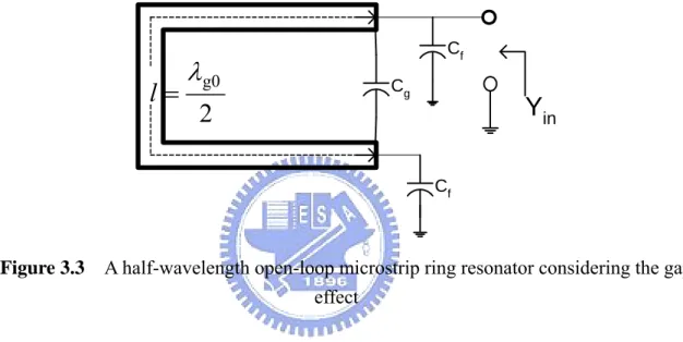
L -j C j R 1 Y 2 0 0 0 in ω ω ω ω ω +∆ − ∆ + ≈ C j 2 R 1 ω ∆ + ≈ (3 . 3) Besides, Figure 3.2 illustrates an open-circuited half-wavelength microstrip ring resonator. Figure 3.3 is equivalent to Figure 3.2 but considering the gap effect. As seen in Figure 3.3, is the physical length of the ring, Cl
g is the gap capacitance, and Cf is the fringe capacitance
caused by fringe field at the both ends of the ring. If the gap size between two open ends of the ring is large, the effect of the gap capacitor Cg for the ring can be ignored, and also the
Y
in2
0
g
l
=
λ
Figure 3.2 A half-wavelength open-loop microstrip ring resonator
Cg Cf Cf
Y
in2
g0λ
=
l
Figure 3.3 A half-wavelength open-loop microstrip ring resonator considering the gap
effect
Because both Cg and Cf are neglected, the input admittance in Figure 3.3 can be wrote as
) tan( Yin = j γl (3 . 4) ) tanh( ) tanh( 1 ) tan( ) tanh( 1 0 j l l l j l Z α β β α + + = (3 . 5)
, where Z0 is characteristic impedance of the microstrip ring, γ is complex propagation
constant, α is the attenuation constant, β is the phase constant and λg0 is the wavelength at
0
ω
ω = . Assume thatl =λg0/2, and letω =ω0 +∆ω. Then, , 0 ω ω π π βl = + ∆ 0 / ) / tan( )
0 0 0 in Z Z 1 Y ω ωπ α + ∆ ≈ l j (3 . 6)
Comparing (3.3) with (3.6), the input admittance of the opened-loop half-wavelength ring microstrip line has the same form as that of a parallel RLC circuit. Therefore, the capacitance in the equivalent circuit is
0 0 2Z C ω π = (3 . 7) The inductance in the equivalent circuit can be obtained from ϖ0 =1/ LC and is given by
C 1 L 2 0 ω = (3 . 8) and the resistance of the equivalent circuit is
g0 0 0 2 R αλ α Z l Z = = (3 . 9) Moreover, the unloaded Q of the resonator denoted by Qu is
g0 0 u L 2 L R Q αλ π α π ω = = = (3 . 10)
3.2 Quality factor design curves
In the equation (3.10), The Qu characterizes the resonant circuit itself, it doesn’t include any
loading effects for the external circuit, so it is named as the unload Q. Figure 3.4 shows the variation of impedance versus frequency for the circuit shown in Figure 3.1. In this figure, the
1
ω and ω are the frequencies which make2 2 =2R2 in
Z . When the frequency at ω and 1 ω , 2 the average power delivered to the circuit is half that at resonance, and in this case, an unload Q of the circuit can be defined by equation (3.11) [12].
2
R
R
ω
0ω
0 1 2ω
ω
ω
−
=
FBW
)
(
Zin
ω
1ω
2ω
Figure 3.4 The circuit responses of impedance magnitude versus frequency for Figure 3.1
FBW 1
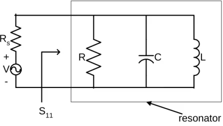
Qu = , for Figure 3.1 and Figure 3.4 (3 . 11) However, in practice, the resonant circuit always is coupled to other circuit such as Figure 3.5. It will reduce the Q factor of the circuit. This Q is called to load Q denoted as QL [12]
which Qe is called the external quality factor, the relationship among Q, QL, and Qe are
e L u Q 1 Q 1 Q 1 = + (3 . 12) In the following section, we will introduce a method to carry out the calculation for the Qe.
Once the Qe is determined, we can have the exact relation between Qu and Qe.
C
L
R
+
V
-R
sresonator
S
11In Figure 3.5, the reflection coefficient or S11 and its phase at the excitation port can be approximated by equation (3.13) (3.14) [13]. ) ω/ω ( j ) ω/ω ( j 0 e 0 e 11 ∆ 2 Q 1 ∆ 2 Q 1 S + − = (3 . 13)
[
( ω/ω )]
1[
e( ω/ω0)]
0 e 1 -Q 2∆ tan Q 2∆ tan S11= − − − ∠ (3 . 14)In the equation (3.14), when∠S11=±900, 2Q 1 0 e m =m
∆
ω ω
. Hence, the absolute bandwidth between the±900point is
e 0 900 Q ω ω ω ω =∆ −∆ = ∆ ± + − (3 . 15)
, where ∆ωm ,∆ω±900 ,∆ω+and ∆ω− are indicated in Figure 3.6. The Qe in (3.15) can be
rewritten to: 0 90 0 e Q ± ∆ = ω ω (3 . 16)
Equation (3.16) and Figure 3.6 provide a convenient method to calculate the Qe, and thus, we
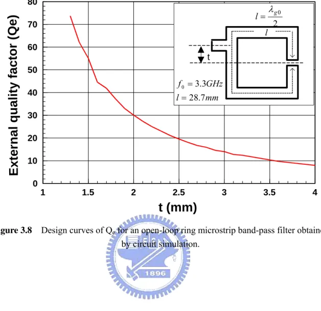
can find the Qe design curve of the circuit in Figure 3.7. Figure 3.8 is the design curves of Qe
obtained by circuit simulation for design of an open-loop ring microstrip band-pass filter. It is noted that the location t of the feed line will affect the external quality factor considerably. To systematically obtain the design curve for Qe, we change progressively the distance t to
calculate Qe by numerical simulation. The variation of Qe against distance t is shown in Figure
3.8. It can be considered as a look up table, that is, we can find out the Qe by specifying the
−
∆
ω
∆
ω
+ o 90 ±∆
ω
180 135 90 45 0 -45 -90 -135 -180 Ph ase o f S 11 (de g ree) 0ω
Figure 3.6 Phase response of S11 for the circuit in Figure 3.5
2
g0λ
=
l
l
t
Rs
+
V
-S
111 1.5 2 2.5 3 3.5 4
t (mm)
0 10 20 30 40 50 60 70 80E
x
te
rn
a
l
q
u
a
li
ty
f
a
c
to
r
(Q
e
)
2 0 g l =λ l t mm l GHz f 7 . 28 3 . 3 0 = =Figure 3.8 Design curves of Qe for an open-loop ring microstrip band-pass filter obtained
by circuit simulation.
3.3 coupling coefficient design curves
In chapter 2, in order to realize the open loop ring band-pass filters, not only the introduced Qe design curves, but also the coupling coefficient design curves are needed. In this section,
3.3.1 electric coupling and magnetic coupling structures
Figure 3.9 is typical coupling structures of coupled microstrip square open-loop resonators. These structures contain different orientations of a pair of identical square open-loop resonators being separated by a spacing S and an offset distance d.
2 g0 λ = l S Cg d 2 g0 λ = l S Cg d (a) (b)
Figure 3.9 Typical coupling structures of coupled microstrip square open-loop resonators (a) Electric coupling structure. (b) Magnetic coupling structure.
Because the open-loop resonators have the maximum electric field at the side with an open-gap and the maximum electric fringing field distribution there, the structure in the Figure 3.9 (a) is called the electric coupling structure. As shown in Figure 3.9 (b), we may conjecture that the coupling is mainly due to the magnetic field caused by the electric currents on the two parallel metal strips. Meanwhile, the faraway of the two open gaps may affect in considerably in this coupling procedure. Thus structure in the Figure 3.9 (b) is called the magnetic coupling structure.
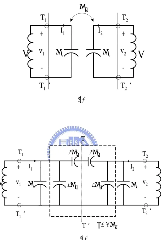
3.3.2 electric coupling design curves
Figure 3.10 (a) is an equivalent lumped-element circuit of electric coupling structure for RF/microwave resonators in figure 3.9 (a), where C and L are the self capacitance and self inductance, so that (LC)-1/2 defines the angular resonant frequency of each uncoupled resonators. Cm represents the mutual capacitance. Because the structure under consideration is
a distributed circuit, the lumped-element equivalent circuit is valid on a narrow-band, namely, near its resonance frequency. Now, we look into reference planes T1-T’1 and T2-T’2, if a
sinusoidal waveform is assumed, this circuit can be regarded as a two-port network and its voltage and current waves satisfy the equation given below:
2 m 1 1 CV C V I = jω − jω (3 . 17) 1 m 2 2 CV C V I = jω − jω (3 . 18)
Form (3.17) and (3.18) the Y-parameters matrix can easily be found by definitions. It is
− − = C C C C Y Y Y Y m m 22 21 12 11 ω ω ω ω j j j j
(3 . 19)
, and using the network theory [12] to the Figure 3.10 (b), we can find that the Y-parameter matrix looked from reference planes T1-T’1 and T2-T’2 in Figure 3.10 (b) is equivalent to
equation (3.19), so an alternative form of the equivalent circuit in Figure 3.10(a) can be obtained and is shown in Figure 3.10(b). This circuit is more convenient to discuss the coupling coefficient of the electric coupling structures.
+
v
1-+
v
2-C
L
L
T
1T
1’
T
2T
2’
I
1I
2C
mC
(a) + v1 -+ v2 -L L T1 T1’ T2 T2’ I1 I2 C C -Cm -Cm m ωC J= m 2C 2Cm T T’ (b)Figure 3.10 (a) An equivalent lumped-element circuit of electric coupling structure (b) An alternative form of the equivalent circuit with an admittance inverter J=ωCm
If we replace a short circuit (electric wall) in the symmetry plane T-T’ in Figure 3.10 (b), the resultant circuit has a resonant frequency such as equation (3.20). This resonant frequency is
lower than that of an uncoupled single resonator. A physical explanation is that when the electric wall is inserted in the symmetrical plane of the coupled structure, the coupling and the resonant frequency becomes:
) C L(C 2π 1 e f m + = (3 . 20) However, if we replace an open circuit (magnetic wall) in the symmetry plane T-T’ in Figure 3.10 (b), the resultant circuit has a higher resonant frequency than that of without coupling
) C L(C 2π 1 f m m − = (3 . 21) Equation (3.20) and (3.21) can be used to find the electric coupling coefficient kE, itis
C C f f f f k m 2 e 2 m 2 e 2 m E + = − = (3 . 22) In the equation (3.21) we can find that kE is identical to the definition of ratio of the coupled
electric energy to the stored energy of uncoupled single resonator.
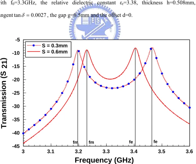
Now, we will induce how use equation (3.22) to find the coupling coefficients of the structure in Figure 3.9 (a). In Figure 3.9(a), if the coupled resonator circuits are over-coupled [1]; that is when the coupling coefficient is greater than the reciprocal of the quality factor of the resonator, the transmission coefficient S21 of the coupling structure can be presented in Figure
3.11. This Figure presents the two split resonant frequencies fe and fm at S=0.3mm or
S=0.6mm. Substituting fe and fm into equation (3.22), the electric coupling coefficients can be
found as shown in Figure 3.12. It is obtained by circuit simulation for the structure of Figure 3.9 (a) on the RO4003C substrate with f0=3.3GHz, the relative dielectric constant εr=3.38,
thickness h=0.508mm, loss tangenttanδ =0.0027, the gap g=0.5mm and the offset d=0. .
3 3.1 3.2 3.3 3.4 3.5 3.6
Frequency (GHz)
-60 -55 -50 -45 -40 -35 -30 -25 -20 -15 -10 -5T
ra
n
s
m
is
s
io
n
(
S
2
1
)
S = 0.3mmS = 0.6mm fe fe fm fmFigure 3.11 The S21 responses for the electric structure when the coupled resonator
circuits are over-coupled
0.1 0.2 0.3 0.4 0.5 0.6 0.7 0.8
S (mm)
0 0.01 0.02 0.03 0.04 0.05 0.06 0.07 0.08E
le
c
tr
ic
c
o
u
p
li
n
g
c
o
e
ff
ic
ie
n
t
(K
E
)
3.3.3 magnetic coupling coefficient design curves
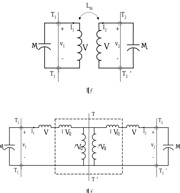
Similar to the electric structure, Figure 3.13 (a) is an equivalent lumped-element circuit of magnetic coupling structure for RF/microwave resonators, where C and L are the self capacitance and self inductance, so that (LC)-1/2 defines the angular resonant frequency of the uncoupled resonators, and Lm represents the mutual inductance. Now, we look into the
reference planes T1-T’1 and T2-T’2, if a sinusoidal waveform is assumed, a two-port network
which may be described by equation (3.23) (3.24).
2 m 1 1 LI L I V = jω + jω (3 . 23) 1 m 2 2 LI L I V = jω + jω (3 . 24) Form (3.23) and (3.24) the Z-parameters matrix can easily be found by definitions. It is
= L L L L Z Z Z Z m m 22 21 12 11 ω ω ω ω j j j j (3 . 25) Similarly, using the network theory [12], Figure 3.13 (b) is an alternative form of equivalent circuits having the same network parameters as those of Figure 3.13 (a). It can be shown that the magnetic coupling between the two resonant loops is represented by an impedance inverter K=ωLm. If the symmetry plane T-T’ in Figure 3.13 (b) is replaced by a short circuit
(or an electric wall), the circuit has a resonant frequency such as equation (3.26). )C L (L 2π 1 f m e − = (3 . 26) From equation (3.26), we could know that the resonant frequency is higher than that of an uncoupled resonator. If the plane T-T’ in Figure 3.13 (b) is replaced by an open circuit (or magnetic wall), it has a resonant frequency such as equation (3.27).
)C L (L 2π 1 f m m + = (3 . 27) and that the resonant frequency shifts toward lower frequency.
L
m+
v
1-+
v
2-C
L
L
T
1T
1’
T
2T
2’
I
1I
2C
(a) + v1 -C T1 T1’ I1 m L 2 + v2 -C T2 T2’ I2 m L 2 L −Lm −Lm L T T’ (b)Figure 3.13 (a) An equivalent lumped-element circuit of magnetic coupling structure (b) An alternative form of the equivalent circuit with an impedance inverter K=ωLm
It is worthy to note that the short circuit bisection (SCB) will increase its resonant frequency, however, the situation of open circuit bisection (OCB) contrasts. This is because that the OCB has the symmetric field distribution and thus the same direction of current flow cause positive mutual inductance Lm, and the total inductance increases accordingly. On the contrary, the
asymmetric current distribution with the SCB case results in negative mutual inductance and thus it decrease the total inductance.
Similarly, equation (3.26) (3.27) can be used to determine the magnetic coupling coefficient Km. it is L L f f f f K m 2 m 2 e 2 m 2 e m + = − = (3 . 28) In this equation we can find km is identical with the definition that is the ratio of the coupled
magnetic energy to the stored energy of uncoupled single resonator. Similarly, in Figure 3.9(b) if the coupled resonator circuits are over-coupled, the transmission coefficient S21 of the
coupling structure can be presented in Figure 3.14. This Figure presents the two split resonant frequencies fe and fm. Substituting fe and fm on equation (3.28), the magnetic coupling
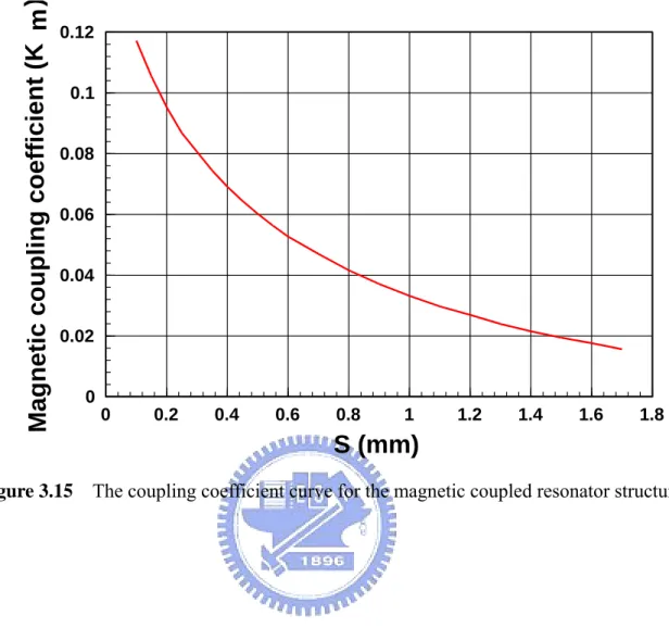
coefficients can be found. Using the method, the magnetic coupling design curves can be found such as Figure 3.15. It is obtained by the circuit simulation on the RO4003C substrate with f0=3.3GHz, the relative dielectric constant εr=3.38, thickness h=0.508mm, loss
tangenttanδ =0.0027, the gap g=0.5mm and the offset d=0.
3 3.1 3.2 3.3 3.4 3.5 3.6
Frequency (GHz)
-45 -40 -35 -30 -25 -20 -15 -10 -5T
ra
n
s
m
is
s
io
n
(
S
2
1
)
S = 0.3mm S = 0.6mm fe fe fm fmFigure 3.14 The S21 responses for the magnetic coupling structure when the coupled
0 0.2 0.4 0.6 0.8 1 1.2 1.4 1.6 1.8
S (mm)
0 0.02 0.04 0.06 0.08 0.1 0.12M
a
g
n
e
ti
c
c
o
u
p
li
n
g
c
o
e
ff
ic
ie
n
t
(K
m
)
Chapter 4
Practical realization of the band-pass filter for
microstrip
In this chapter we will carry out both circuit simulation and experimental studies for the band-pass filters by using microstrip-line. Beside the design of asymmetric feed lines was to employed increase the selectivity of the filters [5].
4.1 The Band-pass filter with symmetric feed lines
Now, we will use the method described previously to design an opened-loop ring band-pass filter. The structure contains symmetric feed lines shown in Figure 4.1. The center frequency f0 = 3.3GHz (λg0/2=28.7mm), frequency bandwidth BW=150MHz (FBW=0.045),
open gap g=0.5mm, order n=2, using RO4003C substrate, relative dielectric constant εr=3.38,
thickness h=0.508mm, loss tangenttanδ =0.0027. By the appendix A, when the n=2, the required g0=1, g1=g2=1.414, g3=1. Substituting they into (2.24) (2.25) (2.26), the external
quality factor can be found as Qe1 =Qe2=31.4 and the electric coupling coefficient is
K12=0.0318. If the Qe1, Qe2 and K12 are substituted into the Qe design curve in the Figure 3.8
and KE design curve in Figure 3.12 respectively, the tapping position and the required gap can
be found as t=2mm and S=0.5mm. Figure 4.2 depicts the calculated and measured insertion loss, while those of return loss are shown in Figure4.3. This filter has a measured insertion loss, 1.67dB, and return loss, 14.5dB, at the center frequency 3.3GHz.
S 2 g0 2 1 λ = + =l l l g 2 l t 1 l l1 2 l
Figure 4.1 The open-loop ring band-pass filter with the symmetric feed lines
2 2.5 3 3.5 4 4.5 5
Frequency (GHz)
-70 -60 -50 -40 -30 -20 -10 0M
a
g
n
it
u
d
e
S
2
1
(
d
B
)
simulation measurementFigure 4.2 The S21 of simulation and measurement for the open-loop ring band-pass
2 2.5 3 3.5 4 4.5 5
Frequency (GHz)
-70 -60 -50 -40 -30 -20 -10 0M
a
g
n
it
u
d
e
S
1
1
(d
B
)
simulation measurementFigure 4.3 The S11 of simulation and measurement for the open-loop ring band-pass
filter with the symmetric feed lines
4.2 The Band-pass filter with asymmetric feed lines
In this section we will introduce a method using asymmetric feed lines, which possesses two transmission zeros. This method has an advantage which can increase the selectivity of the filter on that the filter, however, the size is not increased. Figure 4.4 is a band-pass filter using two hairpin resonators with asymmetric feed lines, where the length of resonator 2l =l1+l2 =λg0/ and the coupling between the two open ends of the resonators is simply expressed by the gap capacitance.
2 0 2 1 g l l l = + =λ 2 l 1 l l2 1 l input output s1 Upper section lower section
Figure 4.4 The filter using two hairpin resonators with asymmetric tapping feed lines
From this configuration, the circuit represents a shunt circuit, which consists of upper and lower sections. The ABCD matrices for the upper and lower section circuit are
3 2 1M M M D C B A upper = (4 . 1) 1 2 3M M M D C B A lower = (4 . 2) If the circuit is lossless, the M1, M2, M3 in the equation (4.1) (4.2) are the ABCD matrices of l1,
l2 and CS respectively such as
= 1 sin( ) cos( ) ) sin( ) cos( 1 1 0 1 0 1 1 l l Z j l jZ l M β β β β (4 . 3) = 1 0 1 2 k Z M (4 . 4) = 1 sin( ) cos( ) ) sin( ) cos( 2 2 0 2 0 2 3 l l Z j l jZ l M β β β β (4 . 5) , where β is the propagation constant, Zk =1/(jωCS) is the impedance of the gap capacitance CS, Z0 is the characteristic impedance of the resonator. By the transformation in
the ABCD parameters to the Y parameter, equation (4.1) (4.2) can be transformed into the Y parameters Yupper and Ylower, respectively. The total Y-parameters of this filter circuit can be
obtained by adding Yupper and Ylower, and the S21 of this filter can be obtained by transforming
Y matrix to S matrix, which is given as:
(
)
4 ) cos( ) cos( ) sin( ) sin( ) cos( 2 ) cos( ) cos( ) sin( 4 2 0 2 1 0 0 2 1 0 0 21 − + + − + = Z l l jZ l Z Z l jZ l l l Z l jZ Z S k k k β β β β β β β β (4 . 6)the transmission zeros can be found by letting S21=0, namely
0 ) cos( ) cos( ) sin( 1 2 0 l +Z l l = jZ β k β β (4 . 7) for a small CS (Zk>>Z0), (4.7) can be approximated as
0 ) cos( )
cos(βl1 βl2 ≈ (4 . 8) substituting β =2πf εeff /c into (4.8),the transmission zeros corresponding to the tapping positions are 4 mc f eff 1 1 ε l = (4 . 9.a) eff 2 2 4 mc f ε l = (4 . 9.b) , where εeff is the effective dielectric constant, m is the mode number and c is the speed of light in free space. Furthermore, Figure 4.5 is an open-loop ring band-pass filter with asymmetric feed lines. This Filter is similar to Figure 4.4, except for the two addition 450 chamfered bends and the coupling gap g between the two open ends of the ring. In [5], the measurement data have verified the two transmission zeros by using (4.9.a) (4.9.b). Here, we also design a filter show in Figure 4.5 to identify equation (4.9). Because this filter has the same structure configuration and design parameters (f0=3.3GHz,FBW=0.045) as that filter in
Figure 4.1, where l=28.7mm, t=1.95mm, S=0.5mm, l1=12.4mm and l2=16.3mm. The
has a measured insertion loss of 1.67 dB and return loss 14.5 dB at center frequency 3.3GHz. The two transmission zeros are f1=3.8125GHz,f2=2.92GHz, respectively, which can be
observed in Figure 4.6. They are very close to the values f1=3.72GHz and f2=2.83GHz
obtained by equation (4.9). In order to refer easily, we put them together and show in Figure 4.8, and we can distinctly find that the transmission zeros are caused by asymmetric feed lines indeed increase the selectivity of the filter.
S 2 0 2 1 g l l l = + = λ g 2 l 1 l t 1 l 2 l
Figure 4.5 The open-loop ring band-pass filter with the asymmetric feed lines
2 2.5 3 3.5 4 4.5 5
Frequency (GHz)
-70 -60 -50 -40 -30 -20 -10 0M
a
g
n
it
u
d
e
o
f
S
2
1
(
d
B
)
simulation measurementFigure 4.6 The S21 of simulation and measurement for the open-loop ring band-pass
2 2.5 3 3.5 4 4.5 5
Frequency (GHz)
-70 -60 -50 -40 -30 -20 -10 0M
a
g
n
it
u
d
e
S
1
1
(
d
B
)
measurement simulationFigure 4.7 The S11 of simulation and measurement for the open-loop ring band-pass
filter with the asymmetric feed lines
2 2.5 3 3.5 4 4.5 5
Frequency (GHz)
-70 -60 -50 -40 -30 -20 -10 0M
a
g
n
it
u
d
e
S
2
1
(
d
B
)
asymmetric feed lines symmetric feed lines
Figure 4.8 The S21 of measurement for the open-loop ring band-pass filter with the
To further increase the selectivity of the filter, we could cascade two sections of the original ones to achieve the purpose. In the following example, we will implement this idea by using four open-loop rings. The design criteria of the circuit is similar to the previous one, namely f0=3.3GHz and FBW=0.045. The needed g0=1=g5, g1=0.7645, g2=1.8478=g3 and
g4=0.7645 can be found in Appendix A with n=4. Substituting they into (2.24)(2.25)(2.26),
The external quality factor Qe1=Qe4=31.4, electric coupling coefficients K12=K34=0.0378,
magnetic coupling coefficients K23=0.0244, and by Qe, KE, Km design curves, the needed
feed line position t=2.1mm and the required gap S1=0.45mm、S2=1.2mm. Figure 4.10
presents the measured results. It is obviously to find that the selectivity of the filter is increased.
s1 s2 s1
Figure 4.9 The layout of the filter using four cascaded open-loop ring resonators with the asymmetric feed lines.
2 2.5 3 3.5 4 4.5 5
Frequency (GHz)
-70 -60 -50 -40 -30 -20 -10 0M
a
g
n
it
u
d
e
(d
B
)
S21S11Figure 4.10 The measured results of the filter using four cascaded open-loop ring resonators with asymmetric feed lines.
In this chapter, we use the theory in the previous chapter to design, fabricate and measure the performance of the filter shown Figure 4.1. In addition, we have also verified that the asymmetric feed lines can drastically enhance the selectivity by introducing two transmission zeros, however, maintain its size. Furthermore, the asymmetric feed lines can be used with higher n filter such as Figure 4.9, and it can increase the selectivity of filter more.
Chapter 5
The design method and realization of the tunable
band-pass Filters
In this chapter we will propose a new method that can switch the resonant frequency of the open loop ring resonator. Beside, we also designed and fabricated some tunable band-pass filters. The results from simulation and measurement will also be presented in this chapter.
5.1 The mechanism of frequency tuning
Figure 5.1 is a conventional method which can electrically tune the resonant frequency of the open loop ring resonator [8]. This method can tune the resonant frequency of the resonator by the tunable capacitance CT of the varactor, and the CT can be tune by the reverse bias.
When the capacitance is increased, the resonant frequency of the resonator will be decreased. In order to have the frequency capability tuning, five devices are needed shown in Figure 5.1, where two capacitors C are the DC choke, two inductors L are the RF choke and one varactor serves as a variable capacitor. This method is simply and conveniently, but its frequency range of tuning is not considerable.
In this section we will propose a new method to switch the resonant frequency of the open loop ring resonator. Figure 5.2 (a) is an equivalent circuit [15] of a varactor connecting to ground. where Lvia is the equivalent inductance of the via hole ground, the parameter Rs, Cp,Ls,
CT is variable capacitance that can varied by the reverse bias. Figure 5.2(b) is the equivalent
circuit that neglect the Rs and Cp, where LT is the sum of the Ls, Lp and Lvia, namely,
. via p s T L L L L = + +
Now, we will apply the varactor equivalent circuit in Figuer 5-2 (b) to Figure 5.3. Figure 5.3 is the new design which can tune resonant frequency of the open loop ring resonator. This circuit not only has wider frequency tuning range, but also has smaller circuit size and fewer devices needed. Only four devices are used in this circuit, a capacitance C is DC choke, a inductance L is RF choke, and two varactors。
When 1/ωCT >ωLT
T
C /
in the structure in Figure 5.3, the X is a negative number and the resonant frequency of this structure is smaller than that without the varactors. On the other hand, when1 ω <ωLT, the X is a positive number and the resonant frequency of this structure is greater than that without the varactors. Once the response curves for CT and X
against frequency, the tunable band-pass filters using this structure can be designed.
Before designing the tunable band-pass filter, we have to find the LT in the Figure 5.4. The
LT method for finding is shown in Figure 5.4, where C and LT form a series LC resonator. The
S21 of this circuit is zero when this series resonator at the resonant frequency, and the LT can
be obtained as follow: C L 1/2π f0 = T (5 . 1)
C C L Vdc L CT
Figure 5.1 The conventional structure for the electrically tunable frequency resonator
Cp Ls Ls Rs CT LP Lvia LT CT (a) (b) varactor Lvia
Figure 5.2 The equivalent circuit for the varactor connect the via hole ground (a)
C Vdc L 1
d
1d
LT CT CT LT T T L j C j jX ω ω + = 1Figure 5.3 The new structure for the electrically tunable frequency resonator
+
V2
-CT
LT
Figure 5.4 The measurement circuit for LT
5.2 The tunable band-pass filter using capacitance reactance X
In section 5-1 we have known that if we could have the response curves for the resonant frequency versus the reactance, the tunable filter can be realized in practice. In this section we will use this new method to design a tunable band-pass filter using capacitance reactance X. In the design we use the substrate (RO4003C), the B-C electrodes of transistor NEC (2SC3356) are taken as anode and cathode of the varactor, the resonant frequency of the ring
resonator without varactor is 2 GHz(λ0/2=47.6mm), BW=50MHz, t=2.5mm, S=0.7mm,
g=0.5mm and the varactor tapping position d1=11.65mm. We find the LT by the circuit Figure
5.4 circuit first. By the measured S21 of Figure 5.1, when C=1.4 pF (reverse bias VR=30V),
the series LC resonant frequency is 5.48GHz and, by equation (5.1) we can find the LT=2.2nH.
Because the capacitance on the varactor was varied from 0.38 to 1.4 pF (VR was varied from
30 to 0 V), the X was varied from -181.76 to -29.19 Ω. Figure 5.5 is the variation of capacitance (reactance) against resonant frequency when the varactor is tapped at d1=11.65mm. The curves present that the resonant frequency f0 is increased by decreased CT
(f0 is increase by decreasing X). Using these curves, we design a tunable band-pass filter such
as Figure 5.6. Figure 5.7 is the layout of this filter. The center frequency can be tuned form 1.86 to 1.5GHz. The insertion loss obtained from simulation and measurement are presented in Figure 5.8 and Figure 5.9 respectively.
1.5 1.55 1.6 1.65 1.7 1.75 1.8 1.85 1.9
Resonant Frequency (GHz)
0.2 0.4 0.6 0.8 1 1.2 1.4T
h
e
c
a
p
a
c
it
a
n
c
e
o
f
v
a
ra
c
to
r
(p
F
)
-200 -180 -160 -140 -120 -100 -80 -60 -40 -20T
h
e
react
an
ce
x
(o
h
m
)
X-frequency C -frequencyTC Vdc L 1 d 1 d LT CT CT L T C Vdc L 1 d 1 d LT CT CT LT S g
Figure 5.6 The new tunable band-pass filter circuit
1.3 1.4 1.5 1.6 1.7 1.8 1.9 2 2.1 2.2 2.3
Frequency (GHz)
-70 -60 -50 -40 -30 -20 -10 0M
a
g
n
it
u
d
e
S
2
1
(
d
B
)
no-varactor VR=30V(C =0.38pF) VR=8V(C =0.56pF) VR=4V(C =0.7pF) VR=2V(C =0.8pF) T T T TFigure 5.8 The simulation of the tunable band-pass filter with the capacitance reactance X
and the BW= 50MHz 1.3 1.4 1.5 1.6 1.7 1.8 1.9 2 2.1 2.2 2.3
Frequency (GHz)
-70 -60 -50 -40 -30 -20 -10 0M
a
g
n
it
u
d
e
S
2
1
(
d
B
)
no-varactor VR=30V(C =0.38pF) VR=8V(C =0.56pF) VR=4V(C =0.7pF) VR=2V(C =0.8pF) T T T TFigure 5.9 The measurement of the tunable band-pass filter with the capacitance reactance X
From Figure 5.8 and Figure 5.9 we can find that the tuning mechanism works when the varactor is present. Beside, we can also find the measured insertion loss is much more than that of simulated case. It should be noted that the resistor is neglected in the circuit simulation. Thus, we may infer that the loss is majorly due to the resistance, shown in Figure 5.2 (a). On the other hand, Figure 5.10 is the simulated result of the filter when the bandwidth is changed to 100MHz (t=3.5mm, S=0.45mm). From this figure, we can find that the insertion loss is decreased by increasing its bandwidth. In order to compare the relations among f0, CT, X, BW,
VR and S21, we arrange the results of the simulation and measurement as listed in table 5-1.
1.3 1.4 1.5 1.6 1.7 1.8 1.9 2 2.1 2.2 2.3
Frequency (GHz
)
-70 -60 -50 -40 -30 -20 -10 0M
a
g
n
it
u
d
e
S
2
1
(
d
B
)
no-varactor VR=36V(C =0.38pF) VR=8V(C =0.56pF) VR=4V(C =0.7pF) VR=2V(C =0.8pF) T T T TFigure 5.10 The measurement of the tunable band-pass filter with the capacitance reactance
Table 5-1 The simulation and measurement results of the tunable band-pass filter with the capacitance reactance X
VR(V) CT(pF) X(Ω) f0(GHz) S21 (dB) (BW=50MHz) S21 (dB) (BW=100MHz)
Simulation 1.99 -2.5 -1.32
measurement
NONE NONE NONE
1.97 -2.69 -1.683 Simulation 1.846 -2.79 -1.52 measurement 30 0.38 -181.76 1.72 -12.197 -6.698 Simulation 1.778 -3 -1.698 measurement 8 0.56 -114.46 1.643 -17.06 -10.088 Simulation 1.726 -3.17 -1.81 measurement 4 0.7 -86.04 1.61 -19.32 -12.098 Simulation 1.69 -3.31 -1.93 measurement 2 0.8 -71.83 1.59 -21.89 -14.988
Further, it should be mentioned that the resonant frequency not only depends on X but also on d1 in the Figure 5.3. Figure 5.11 is the variation of d1 versus the resonant frequency.
That is, in addition to the reactance of the varactor, the distance d1 can also provide an extra