Properties of Mg activation in thermally treated GaN:Mg films
C. F. Lin, H. C. Cheng, C. C. Chang, and G. C. ChiCitation: Journal of Applied Physics 88, 6515 (2000); doi: 10.1063/1.1308097
View online: http://dx.doi.org/10.1063/1.1308097
View Table of Contents: http://scitation.aip.org/content/aip/journal/jap/88/11?ver=pdfcov Published by the AIP Publishing
Articles you may be interested in
Investigation on the compensation effect of residual carbon impurities in low temperature grown Mg doped GaN films
J. Appl. Phys. 115, 163704 (2014); 10.1063/1.4873957
Effects of KrF (248 nm) excimer laser irradiation on electrical and optical properties of GaN:Mg J. Vac. Sci. Technol. B 21, 641 (2003); 10.1116/1.1545732
Electrical and optical properties of beryllium-implanted Mg-doped GaN J. Appl. Phys. 92, 1881 (2002); 10.1063/1.1494110
Strong acceptor density and temperature dependences of thermal activation energy of acceptors in a Mg-doped GaN epilayer grown by metalorganic chemical-vapor deposition
Appl. Phys. Lett. 80, 1001 (2002); 10.1063/1.1448666
Structural defects and microstrain in GaN induced by Mg ion implantation J. Appl. Phys. 83, 5992 (1998); 10.1063/1.367465
Properties of Mg activation in thermally treated GaN:Mg films
C. F. Lina) and H. C. ChengDepartment of Electronics Engineering and Institute of Electronics and Semiconductor Research Center, National Chiao Tung University, Hsinchu 30049, Taiwan, Republic of China
C. C. Chang and G. C. Chi
Department of Physics, National Central University, Chungli, Taiwan, Republic of China 共Received 5 January 2000; accepted for publication 8 July 2000兲
The Mg acceptors of GaN films are activated as p-type GaN with rapid thermal annealing 共RTA兲 and furnace treatments. The GaN:Mg films are activated successfully by using the RTA system below 1000 °C for 1 min. After the RTA treatment, we observed a sharper linewidth and stronger emission intensities from donor to acceptor peaks in the photoluminescence spectra. By comparing the electrical properties of GaN:Mg films at optimum conditions made with RTA 共800 °C兲 and furnace共700 °C兲 treatments, we find similar activated hole concentration and a higher hole mobility for GaN:Mg films with RTA treatment at 800 °C. A higher bulk resistivity caused by increasing nitrogen vacancies is found at higher temperature and longer time RTA treatments. Faster treatment times and lower temperatures for the GaN:Mg films were achieved with the RTA activation process. © 2000 American Institute of Physics.关S0021-8979共00兲04120-7兴
I. INTRODUCTION
Gallium nitride is a direct wide-band gap semiconductor, which has attracted considerable interest when applied in blue, green and ultraviolet light-emitting diodes共LEDs兲. Pio-neering efforts have created p-type GaN films,1 which are one of the keys to the success of GaN-based light-emitting devices such as LEDs2 and laser diodes 共LDs兲.3 Nakamura et al.4 reported that low-resistivity p-type GaN films were obtained through N2-ambient thermal annealing or low-energy electron beam irradiation 共LEEBI兲 treatments. Sug-iura et al. noted that low-resistivity p-type GaN:Mg films had been obtained through H2-free growth without any
posttreatments.5 And Miyachi et al.6reported the activation process in GaN:Mg by annealing with minority carrier injec-tion. Prior studies7–9 show that the Mg–H complex10 in GaN:Mg films can be activated with an activation time in excess of 5 min, and with temperatures above 1000 °C in the rapid thermal annealing 共RTA兲 system. The high-temperature process affected the quality of the InGaN layers in the multiple quantum well共MQW兲 LED structures during the LED fabrication process. In this experiment, a lower tem-perature and a faster RTA activation process were success-fully achieved to get p-type GaN. The activation process for Mg-doped GaN epitaxial layers varied for the two different thermal treatments: the furnace and the RTA system. The activation temperatures were changed during both treat-ments. The electrical and optical properties of the activated GaN:Mg epitaxial layers will be compared in the furnace and RTA annealing systems later in this work.
II. EXPERIMENTS
The GaN:Mg films were grown by metalorganic chemi-cal vapor deposition 共MOCVD兲 on polished optical-grade
C-face 共0001兲 sapphire substrates. A sapphire substrate was placed on a graphite susceptor in a horizontal type reactor with a rf heater. Trimthylgallium 共TMGa兲, ammonia (NH3)
and bis-cyclopentadienyl-magnesium (Cp2Mg) were used as
the Ga, N and Mg sources, respectively. After growing the GaN buffer layer at 525 °C, the temperature was raised to 1025 °C to grow a thin undoped GaN epitaxial layer 共as the second buffer layer兲 and a third 2m Mg-doped GaN layer was also grown, at 1025 °C, for this experiment. The as-grown GaN:Mg films were activated in N2 ambient for 30
min with varying temperatures of 600, 700, 800 and 850 °C in the furnace system. The other series of Mg-doped GaN was activated by the RTA system and the temperature was varied from 600 to 960 °C for 1 min. The electric and optical properties in both series of GaN:Mg films were measured by the Hall effect and photoluminescence 共PL兲 measurements. A Ni/Au共150 Å/2000 Å兲 metal layer was used as the ohmic contact. Using the van der Pauw method in the Hall effect measurement, in each contact, ohmic properties were ob-served for all of the activated GaN:Mg films from the current versus voltage (I – V) curves.
III. RESULTS AND DISCUSSION
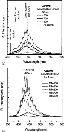
PL spectra for the GaN:Mg films were excited with a 40 mW He–Cd laser and measured at room temperature. We observed that the typical PL emission peaks at 441 nm were caused by the transitions from the shallow donors to the Mg acceptor pairs 关donor–acceptor pairs 共DAPs兲兴. Also seen from the PL spectra from furnace-treated samples were the donor bound excitons共365 nm兲 peaks of GaN and the accep-tor bound exciton 共395 nm兲 peak of GaN:Mg. Fabry–Pe´rot fringe signals were also clearly distinguished in the PL spec-tra, and these signals showed the mirror-like, uniform, high crystal quality of the GaN:Mg films that were used in this experiment. The DAP peaks were fixed at 441 nm even when a兲Electronic mail: [email protected]
6515
0021-8979/2000/88(11)/6515/4/$17.00 © 2000 American Institute of Physics
we varied the activation temperatures in the furnace system. From the PL spectra, we saw that for the GaN:Mg films with the RTA treatment, the wavelength of DAP peaks shifted to high energy from 446 to 430 nm by increasing the activation temperatures. The PL peak located at 430 nm was caused by a free electron–acceptor transition by the increment of ion-ized electrons from the donor at high activation tempera-tures. The transition process changed from a DAP to a free electron–acceptor transition in the PL spectra. The PL peak’s movement from a DAP to acceptor bound excitons was about 104 meV. From Figs. 1共a兲 and 1共b兲, one can see that the luminescence intensity of the GaN:Mg with RTA activa-tion was higher than that with furnace activaactiva-tion. The emis-sion efficiency of GaN:Mg films with RTA activation was also higher than with furnace activation, and the emission efficiency had a stronger effect on the GaN-based optical devices. The full width of half maximum 共FWHM兲 of the DAP transition peaks was sharper, from 56.6 to 42.6 nm, by increasing the activation temperature in the RTA system. When the activation temperature was above the optimum temperature 共800 °C兲, the FWHM and emission intensity of the PL peak were broadened and weakened by the thermal
damage on the surface states of the GaN:Mg films. The peak wavelength and FWHM of the PL spectra in Fig. 2 indicate that the optimum activation temperatures are located at 700 and 800 °C in the furnace and RTA systems. The FWHM and emission intensity of the DAP peaks with the RTA
共FWHM⫽42.6 nm兲 treatment are sharper and stronger than
those of the GaN:Mg films in the furnace treatment
共FWHM⫽60 nm兲. These sharper and stronger PL spectra
with the RTA treatment have a greater effect on output power during LED operation.
To analyze the electrical properties of the Mg-doped GaN films, such as the hole mobility, the hole concentration and the bulk resistance, we used the Hall effect measure-ment. From Fig. 3, one can see that the maximum hole con-centration of 3.6⫻1017cm⫺3 and hole mobility of 9.2 cm2/V s were obtained with the furnace treatment at 700 °C annealed for 30 min. Also, the lower bulk resistivity of 1.6
⍀ cm Mg-doped GaN with 700 °C furnace treatment is
shown in Fig. 4. For the RTA activation process, the hole concentration increased and the hole mobility reduced by increasing the activation temperatures from 600 to 900 °C. FIG. 1. PL spectra of activated Mg-doped GaN films with various activation
temperatures using furnace共a兲 and RTA 共b兲 systems. The Mg-related peaks in both systems are located at a wavelength of 410 nm. The typical PL peak of GaN:Mg films was due to the transition between donor and acceptor.
FIG. 2. Wavelength and FWHM of Mg-related PL peaks as a function of activation temperatures treated in furnace and RTA systems.
FIG. 3. Hole mobility and hole carrier concentration of activated GaN:Mg films shown as a function of activation temperatures. The active acceptor concentration increased with the activation temperature and slightly de-creased over the optimum activation temperature in both the furnace and RTA systems.
6516 J. Appl. Phys., Vol. 88, No. 11, 1 December 2000 Linet al.
For good device performance, the p-type GaN must have a high hole concentration, a high mobility and a lower bulk resistance. From the data we saw that the optimum activation for the electric properties of the GaN:Mg films with the RTA treatment was located at 800 °C. The hole concentration, mo-bility and bulk resistance were 2.4⫻1017cm⫺3, 12 cm2/V s and 1.6⍀ cm for this p-type GaN film. In the RTA activation process, the hole concentration and hole mobility were slightly decreased when the activation temperature was above the optimum. The Mg activation efficiency remained the same although we varied the activation temperature in the optimum temperature region. However, outside of this optimum region, it did change. Both the RTA and furnace activation processes have lower activation efficiencies when above the optimum annealing temperatures shown in Fig. 3. We compared the optimum electrical properties of GaN:Mg films with the RTA and furnace activation systems, and the hole concentration was similar in both, but the hole mobility was higher for the GaN:Mg films with the RTA treatment. The bulk resistance observed from the Hall effect measure-ment was located between 1 and 2 ⍀ cm with a furnace treatment above the 700 °C activation temperature, but this bulk resistance had a stronger fluctuation caused by a varia-tion in the activavaria-tion temperatures with the RTA system. The optimum bulk resistance for the GaN:Mg film was treated at 800 °C RTA annealing. However, the resistivity increased by raising the activation temperatures. The Ni/Au metal con-tacts on the GaN:Mg films with the RTA activation process all show ohmic properties. The surface states of GaN:Mg films were damaged under higher temperature RTA treat-ments, and the nitrogen vacancy increased during these same high-temperature and long annealing time treatments. The contact resistance on the surface damaged GaN:Mg films was increased by the high bulk resistance of the films. The GaN:Mg films were heavily damaged under high tempera-tures and long treatment times in the RTA process. The bulk resistance was similar at about 1.6⍀ cm under optimum con-ditions for the RTA and furnace systems, and a higher hole mobility of 12 cm2/V s was obtained from the RTA treatment
for the p-type based device. The RTA activation system pro-vided a fast, low-temperature process with better electric properties for the p-type GaN:Mg films.
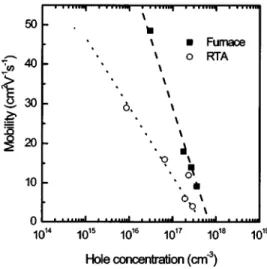
The hole mobility as a function of the hole concentration is shown in Fig. 5. The electric properties of a series of activated GaN:Mg films in the furnace system is located at the higher slope line in Fig. 5, and the other series of GaN:Mg films activated in RTA system is located on the lower slope line. When the hole concentration increases, the mobility in both series of GaN:Mg films is decreased by the effect of ionization scattering of the hole acceptors. In this experiment, the Mg-doped GaN films obtained a similar car-rier concentration and bulk resistivity and a higher hole mo-bility with an 800 °C RTA treatment.
IV. CONCLUSIONS
GaN:Mg films were activated by furnace and RTA sys-tems in this experiment. The GaN:Mg films were activated in a N2ambient for 30 min by varying the temperatures in the
furnace system. In the RTA system, the activation tempera-tures were varied from 600 to 960 °C for 1 min in a N2
ambient. The FWHM and the emission intensity of the DAP peaks we saw from the PL spectra of the GaN:Mg films at room temperature with the RTA treatment were sharper and stronger than those with the furnace treatment. In the tradi-tional furnace thermal treatment, the hole concentration and mobility were 3.6⫻1017cm⫺3and 9.2 cm2/V s, respectively, with a 700 °C optimum activation temperature. The activated hole concentration was 2.4⫻1017cm⫺3, the bulk resistivity
was 1.6⍀ cm and the hole mobility was 12 cm2/V s with an 800 °C RTA treatment. Comparing the optimum electric properties of GaN:Mg films in the RTA共at 800 °C兲 and fur-nace 共at 700 °C兲 activation systems, the active hole concen-trations were similar and the hole mobility was higher for the GaN:Mg films with 800 °C RTA treatment. The surface states of the GaN:Mg films were damaged at high-temperature RTA treatments. When the hole concentration increased, the mobility in both series of GaN:Mg films FIG. 4. Bulk resistivity of RTA and furnace treated GaN:Mg films as a
function of RTA treatment temperatures. The bulk resistivity of GaN:Mg films is about 1–2⍀ cm higher than 700 °C with furnace treatment. The bulk resistivity had a stronger fluctuation with RTA treatment.
FIG. 5. Hole mobility as a function of the hole concentration varied with activation of the furnace and RTA systems.
decreased because of the ionic acceptor scattering effect. In this experiment, the sharper and stronger PL spectra with the RTA treatment more strongly affected the output power dur-ing the homojunction blue LED operation. The result is that the RTA activation system provides a fast, low-temperature process with better electric properties for p-type GaN:Mg activation.
ACKNOWLEDGMENTS
This research was supported by the National Science Council of Taiwan, Republic of China, under Contract No. NSC 89-2215-E-009-069. Technical support by the Semi-conductor Research Center at National Chiao Tung Univer-sity is also acknowledged.
1S. Nakamura, T. Mukai, M. Senoh, and N. Iwasa, Jpn. J. Appl. Phys., Part
2 31, L139共1992兲.
2S. Nakamura, T. Mukai, and M. Senoh, Jpn. J. Appl. Phys., Part 1 30,
1998共1991兲.
3S. Nakamura, M. Senoh, S. Nagahama, N. Iwasa, T. Yamada, T.
Mat-sushita, H. Kiyoku, and Y. Sugimoto, Jpn. J. Appl. Phys., Part 2 35, L74
共1996兲.
4S. Nakamura, N. Iwasa, M. Senoh, and T. Mukai, Jpn. J. Appl. Phys., Part
1 31, 1258共1992兲.
5L. Sugiura, M. Suzuki, and J. Nishio, Appl. Phys. Lett. 72, 1748共1998兲. 6
M. Miyachi, T. Tanaka, Y. Kimura, and H. Ota, Appl. Phys. Lett. 72, 1101共1998兲.
7C. J. Eiting, P. A. Grudowski, J. Park, D. J. H. Lambert, B. S. Shelton, and
R. D. Dupuis, J. Electrochem. Soc. 144, L219共1997兲.
8W. Go¨tz, N. M. Johnson, J. Walker, D. P. Bour, and R. A. Street, Appl.
Phys. Lett. 68, 667共1996兲.
9C. W. Wang, J. Y. Liao, C. L. Chen, and W. K. Lin, J. Vac. Sci. Technol.
B 17, 1545共1999兲.
10W. Go¨tz, N. M. Johnson, J. Walker, D. P. Bour, H. Amano, and I.
Akasaki, Appl. Phys. Lett. 67, 2666共1995兲.
6518 J. Appl. Phys., Vol. 88, No. 11, 1 December 2000 Linet al.