2332 Journal of The Electrochemical Society, 147 (6) 2332-2336 (2000) S0013-4651(99)10-007-7 CCC: $7.00 © The Electrochemical Society, Inc.
There are many techniques for achieving low dielectric materials. These materials can be deposited on the substrate either by spin-on or by chemical vapor deposition (CVD). Spin-on materials have sev-eral advantages different from those of CVDs, such as better gap fill-ing capability, better planarization, lower cost, and easier use. The most studied low-k materials are fluorinated SiO2 and inorganic spin-on-glass (SOG). Fluorinated SiO2has a dielectric constant of 3.1, but it does not meet the need of subquarter micrometer tech-nologies. Inorganic SOG contains much silanol (Si-OH), and tends to crack due to large shrinkage during curing steps.1,2The organic SOP results in several beneficial film properties, e.g., low dielectric constant, decreased silanol content low moisture absorption, in-creased crack resistance, and excellent planarization.
Currently, Cu and spin-on organic polymer (SOP) are the leading candidates for metal and dielectric materials. Device integration with lower dielectric constant material and lower resistance Cu film is capable of improving its performance and reducing the intercon-nection delay.3-5The major drawback of the next generation of Cu interconnects is the fast diffusion speed in the traditional oxide layer and in the low dielectric constant materials.6,7A thin barrier metal is inserted between the Cu and the dielectric layer, which is a conven-tional method for blocking Cu diffusion. This barrier metal-free structure6,8,9for SiON interlevel dielectrics has been proved to be an effective block for Cu diffusion and reduction of resistance-capaci-tance (RC) delay time. The other problem with organic SOP materi-als is the oxygen plasma stripping photoresist process,10,11which causes significant damage to organic low dielectric material, thus limiting its interlevel dielectric application. NH3plasma treatment can effectively improve the barrier effect against Cu and the ashing resistance at the same time. This method brought many good results with the exception of a little higher dielectric constant and leakage current than as-cured samples.
In this study, a carbon-containing silicon nitride was achieved by NH3plasma exposed to organic SOP film. This layer has shown a much greater improvement in the barrier effect and in ashing resistance.
Experimental
The organic SOP (Allied Signals X-720) was spun on (100) 4-7V cm p-type Si wafers. It is based on methyl(CH3) phenyl(C6H5)
silsesquioxane. The thickness of SOP is approximate 200 nm after curing at 4008C for 60 min. The process steps used in this study are
1. A 200 nm SOP was spun on Si substrate.
2. SOP was treated with NH3plasma by plasma-enhanced chem-ical vapor deposition (PECVD) technique. The substrate tempera-ture is 3008C, the pressure is 40 Pa, the flow rate of both NH3and H2is 300 sccm, and the rf power is 300 W.
3. The ashing treatment was performed by a barrel reactor asher with oxygen plasma. The pressure is 0.5 Torr, the rf power is 100 W, the rf frequency is 13.56 MHz, and the exposure time is 10 min.
4. The Cu film of 200 nm was deposited on the different samples by sputter and then formed an metal insulator semiconductor (MIS) capacitor structure.
Several different measurement techniques were used to measure the as-deposited and annealed samples. Fourier transform infrared (FTIR) spectroscopy was used to help us understand the molecular structure of material. The atomic concentrations of Cu ion in the SOP film were examined by secondary ion mass spectrometry (SIMS). The percentage of nitrogen in SOP was measured by X-ray photoelectron spectroscopy (XPS) technique. The dielectric constant was calculated from the capacitance-voltage (C-V) plots using MIS structure. The leakage current was measured by precision semicon-ductor parameter analyzer (HP 4156A).
Results and Discussion
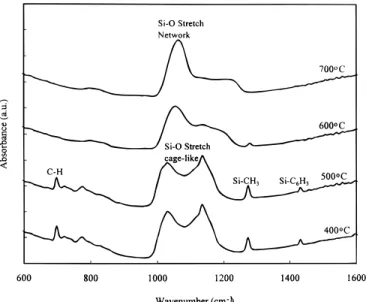
Figure 1 shows the FTIR spectra of SOP after different curing temperatures. When cured above 5008C, the spectra indicate that the peaks of organic groups such as Si-CH3and Si-C6H5get lower with increasing temperature and even disappear at 7008C. The organic groups started to be decomposed at 500,6008C,12,13 curing at 4008C seems not to cause a change of Si-C content in the SOG film. This figure also indicates that the cage-like structure starts convert-ing to network structure at 6008C, and it shows a near-stoichiomet-ric SiO2after curing at 7008C for 1 h. The low dielectric constant properties are related to the cage-like structure in the SOP film and disappear after annealing at high temperatures. Figure 2 shows that the thickness of the SOP film started to shrink significantly after cur-ing at 6008C for 1 h. This is consistent with the organic group that started to decompose in the temperature range of 500,6008C as shown in Fig. 1. The shrinkage of X-720 SOP is very small when an-neals are below 5008C, which implies that this organic SOP has the advantages of better planarization and higher cracking resistance.
A Novel Pretreatment Technology for Organic Low-Dielectric Material to
Suppress Copper Diffusion and Improve Ashing Resistance
Kow-Ming Chang,
aI-Chung Deng,
a,b,* Yao-Pin Tsai,
bChan-Yang Wen,
aSy-Jer Yeh,
aShih-Wei Wang,
cand Jin-Yea Wang
aaDepartment of Electronic Engineering and Institute of Electronics, National Chiao Tung University and
National Nano Device Laboratory, Hsinchu, Taiwan
bDepartment of Electronic Engineering, Kuang Wu Institute of Technology and Commerce, Taipei, Taiwan cWordwide Semiconductor Manufacturing Corporation, Hsinchu, Taiwan
A new novel pretreatment technology for integration of organic low-dielectric material in copper interconnects for ultralarge scale integration applications is developed. Using NH3plasma treatment, two extremely important advantages were achieved in spin-on
organic polymer (SOP), including the reduction of copper diffusion and the improvement of ashing resistance. A copper/SOP/Si capacitor structure is used to study the electrical characteristics of SOP film after ashing treatment or postanneal. Higher barrier capability and better ashing resistance can be achieved by the SOP layer after NH3plasma treatment. After annealing at 5008C for
60 min, secondary ion mass spectroscopy depths profile shows that the Cu atoms do not penetrate into the SOP when they are pre-treated by NH3plasma. Furthermore after the ashing step, the carbon atoms in the SOP film almost remain the same when they are
pretreated by NH3plasma. On the other hand, the concentration of carbon in as-cured SOP is no longer seen. The reason of
improv-ing ashimprov-ing resistance and better barrier capability was due to the organic polymer film rearrangimprov-ing to form a carbon-containimprov-ing sil-icon nitride film.
© 2000 The Electrochemical Society. S0013-4651(99)10-007-7. All rights reserved. Manuscript submitted October 1, 1999; revised manuscript received February 22, 2000.
In the integrated circuit process, photoresist stripping (ashing) by using oxygen plasma is inevitable. Organic SOP will suffer rapid oxidation during the ashing step. Furthermore, the carbon content in the organic SOP will be removed. Figure 3a shows the FTIR spectra of the as-cured MSQ film after ashing for different times. The organ-ic groups in this film gradually disappeared with increasing ashing time. The disappearance of cage-like structure correlated well with the shrinking of film thickness and the increase of dielectric con-stant. The silanol (Si-OH) peak was also present at 928 cm21which implied an increase in the absorption of moisture in the SOP film. The presence of silanol and water was undesirable and would cause reliability problems, such as poisoning via hot carrier degradation. Figure 3b shows that the FTIR spectra of the H2plasma pretreatment sample reveal the same results as the as-cured one. The organic group in the SOP film also decomposed after the ashing step. This indicated that the H2plasma do not improve the characteristics of ashing resistance. In Fig. 3c, however, the organic SOP can effec-tively increase the ashing resistance of the SOP after an NH3plasma treatment for 10 min. The spectra of organic SOP remain unchanged after an ashing treatment for 10 min.
Figure 1. FTIR spectra of the cured SOP after thermal treatment at different temperatures for 1 h.
Figure 2. The thickness variation of SOP film after annealing at different temperatures for 1 h.
Figure 3. FTIR spectra of (a, top) as-cured SOP after ashing for different times, (b, middle) NH3plasma pretreated SOP after ashing for 10 min, (c,
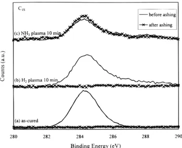
2334 Journal of The Electrochemical Society, 147 (6) 2332-2336 (2000) S0013-4651(99)10-007-7 CCC: $7.00 © The Electrochemical Society, Inc. Figure 4 shows the X-ray photoemission spectroscopy (XPS)
spectra of carbon in organic SOP film under different conditions be-fore and after ashing treatments. The carbon peak of C1Sat 284.8 eV
is not found in the XPS spectra of the as-cured and H2plasma treat-ed samples. It coincides with those of the organic groups removtreat-ed during the ashing step as shown in Fig. 3a and b. After NH3plasma treatment, the carbon content almost remains unchanged, and a new peak of N1Swas observed at 400 eV. The incorporation of nitrogen
atoms increases with increasing exposure time. The N1Speak implies
that a nitride layer of SiCON is formed after NH3plasma treatment. This nitride layer plays a major role in improving the ashing resis-tance.
The formation of nitride film also improves the electrical charac-teristics of SOP. Figure 5a shows the leakage current density of the as-cured MIS capacitors. It shows a three orders increase in leakage current after the ashing step. Comparing the H2and NH3 plasma-treated samples, in Fig. 5b and c, the sample with preplasma-treated SOP by H2plasma shows an increase of leakage current, which is smaller than that of the SOP layer after NH3plasma treatment. However, the leakage current of the NH3-plasma treated sample after ashing plas-ma exposure is better than the others. Although the sample of SOP after NH3 plasma treatment reveals a little higher leakage current and dielectric constant than that of SOP after H2plasma treatment, the NH3plasma can effectively improve the ability of resisting the ashing oxygen plasma. After the ashing step, the NH3 pretreated sample had a one order lower leakage current than that of the H2 plasma-treated sample. Figure 5c also demonstrates that only the sample with 20 min NH3plasma pretreatment shows no leakage cur-rent degradation after the ashing step. The dielectric constant of this sample is 2.85. However, more plasma exposure time results in a higher dielectric constant and higher leakage current. Even though the ashing step causes more damage on the surface of the NH3 plas-ma sample pretreated for 10 min, the 20 min NH3plasma pretreated sample shows the same leakage current level after the ashing step. Thus, the sample of pretreated by NH3plasma for 10 min demon-strated better characteristics than the others. Therefore, we chose this condition to study its characteristics further.
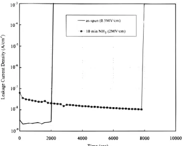
After annealing at 350 and 4008C for 60 min, as shown in Fig. 6, we compare the leakage current density of Cu/as-cured SOP/Si struc-ture with the Cu/SOP/Si strucstruc-ture in which SOP film was exposed in NH3plasma for 10 min. This figure shows that the SOP after NH3 plasma treatment has a lower leakage current than the others. This phenomenon implies that the formation of nitride film can effective-ly improve the barrier effect against Cu diffusion. Moreover, after annealing at 3508C for 60 min, the NH3plasma-treated SOP sample
shows a lower leakage current than the as-treated one. This is due to fact that the damage in SOP is annealed-out after the annealing
treat-Figure 4. C1SXPS spectra of (a) as-cured SOP, (b) H2plasma pretreated
SOP, and (c) NH3plasma pretreated SOP before and after ashing treatments.
Figure 5. Comparing the leakage current density of (a, top) as-cured SOP, (b, middle) H2plasma pretreated SOP, and (c, bottom) NH3plasma
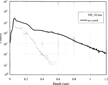
ment. Figure 7 compares the Cu depth profile of the as-cured SOP and NH3treatment SOP after annealing at 4008C for 1 h. The results show an obvious improvement after NH3treatment. Comparing sam-ples with differently treated conditions above, only the sample with NH3plasma treatment successfully blocks the Cu diffusion.
Figures 8a and b indicate the electrical breakdown field (EBD)
distributions of the as-cured samples and NH3plasma-treated sam-ples after annealing at various temperatures, respectively. The SOP layer shows a great improvement of breakdown voltage after the NH3plasma treatment. In Fig. 8a, the as-cured SOP sample shows a significant degradation in breakdown field after postannealing at 3508C for 60 min. We suggested that the degradation of breakdown field was due to Cu atoms diffusing into SOP film through thermal excitement. In the case of the samples treated by NH3 plasma, it shows an improvement in electrical breakdown field after post-annealing at 3508C. The difference between the as-cured and the NH3-treated samples is a layer of carbon-containing silicon nitride film on the surface of SOP after the NH3plasma treatment. It is very clear that the higher breakdown field is attributed to the SOP film which becomes denser and damage in the SOP film was annealed out after postannealing.
Figure 9 shows the influence of the time to failure (TTF) of Si/SOP/Cu capacitors that can be used as indicators of barrier qual-ity. The effect of the electric field on copper transport is also shown for different samples when the temperature was measured at 1508C. In this figure of the TTF stress of SOP, it was found that the sample after NH3plasma treatment showed much greater improvement than the as-cured sample. Even if we applied four times the electric field to the NH3plasma sample, it still showed about four times longer TTF time than the as-cured sample. The NH3plasma-treated sample shows a “self-healing” phenomena (the leakage current spikes up and down) which are sometimes observed in TTF testing. These phe-nomena are due to nonuniform diffusion of copper.14Based on these measured data, the NH3plasma treatment is an excellent method for improving the quality of SOP.
Conclusion
The NH3and H2plasma treatments were studied to improve the quality of carbon containing organic low dielectric materials (e.g., X-720), a spin-on low-k material. The NH3plasma treatment pro-vides an efficient method for improving the ashing resistance and the blocking of Cu diffusion. On the other hand, this film does not achieve any notable improvement after it is treated by H2plasma. The X-720 film also shows a small thickness shrinkage after the cur-Figure 6. The leakage current density of as-cured SOP and NH3plasma
pre-treated SOP samples after annealing at 350 and 4008C for 1 h.
Figure 8. Weibull plot of electrical breakdown field (EBD) distributions for (a, top) as-cured SOP, (b, bottom) NH3plasma pretreated SOP as capacitor
dielectric layers after different thermal treatment conditions.
Figure 7. Comparing the Cu depth profiles of as-cured and NH3plasma
2336 Journal of The Electrochemical Society, 147 (6) 2332-2336 (2000) S0013-4651(99)10-007-7 CCC: $7.00 © The Electrochemical Society, Inc.
ing step. From the electrical measurements and SIMS and XPS analyses, we found that the characteristics of X-720 demonstrated a dramatic improvement after NH3plasma treatment. These improve-ments are due to a nitride film formed after the NH3plasma treat-ment. From the experimental results, the NH3plasma treatment is an excellent approach for improving the characteristics of X-720.
Acknowledgments
This work was supported by National Science Council under grant NSC88-2215-E-009-046.
National Chiao Tung University assisted in meeting the publication costs of this article.
References
1. C. Chiang and D. B. Fraser, in Proceedings of the VLSI Multilevel Interconnect Conference, VMIC, p. 397 (1989).
2. S. K. Gupta, Mater. Res. Soc. Symp. Proc., 108, 275 (1988).
3. C. S. Pai, P. W. Diodato, and R. Liu, in Proceedings of International Interconnect Technology Conference, IITC, p. 244 (1999).
4. M. Igarashi, A. Harada, H. Amishiro, H. Kawashima, N. Morimoto, Y. Kusumi, T. Saito, A. Ohsaki, T. Mori, T. Fukada, Y. Toyoda, K. Higashitani, and H. Arima, in Tech. Dig. Int. Electron Devices Meet., p. 829, IEEE (1998).
5. B. Zhao, D. Feiler, V. Ramanathan, Q. Z. Liu, M. Brongo, J. Wu, H. Zhang, J. C. Kuei, D. Young, J. Brown, C. Vo, W. Xia, C. Chu, J. Zhou, C. Nguyen, L. Tsau, D. Dornish, and L. Camilletti, in VLSI Dig. Technical Papers, p. 28 (1998). 6. D. S. Gardner, J. Onuki, K. Kudoo, Y. Misawa, and Q. T. Vu, Thin Solid Films, 262,
104 (1995).
7. K. Shanker and J. R. MacDonald, J. Vac. Sci. Technol., A, 5, 2894 (1987). 8. K. Migagi, H. Ishikawa, T. Usami, M. Suzuki, K. Inoue, N. Oda, S. Chikaki,
I. Sakai, and T. Kikkawa, in Tech. Dig. Int. Electron Devices Meet., p. 365, IEEE (1996).
9. G. M. Adema, L. T. Hwang, G. A. Rinne, and I. Turlik, IEEE Trans. Comp., Hybrids, Manuf. Tech., 16, 53 (1993).
10. S. Ito, Y. Homma, and E. Sasaki, J. Vac. Sci. Technol. A, 9, 2696 (1991). 11. M. Matsuura, Y. Ii, K. Shibata, Y. Hayashide, and H. Kotani, in Proceedings
Inter-national VLSI Multilevel Interconnect Conference, VMIC, p. 113 (1993). 12. M. P. Woo, J. L. Cain, and C. O. Lee, J. Electrochem. Soc., 137, 196 (1990). 13. P. L. Pai, A. Chetty, R. Roat, N. Cox, and C. Ting, J. Electrochem. Soc., 134, 2829
(1987).
14. G. Raghavan, C. Chiang, P. B. Ander, S. M. Tzeng, R. Villasol, G. Bai, M. Bohr, and D. B. Fraser, Thin Solid Films, 262, 168 (1995).
Figure 9. Influence of time to failure of Si/SOP/Cu capacitors after NH3 plasma pretreatment for 10 min.