國 立 交 通 大 學
奈 米 科 技 研 究 所
碩 士 論 文
奈米金表面修飾增加鍵結效率並應用於光電生物感
測器之研究
Nanoscale-Based Transduction for High-Efficiency of Biomolecular
Interactions and Optoelectronic Biosensor Application
研 究 生:游群芳
Chun-Fang Yu
指導教授:柯富祥 教授
Prof. Fu-Hsiang Ko
奈米金表面修飾增加鍵結效率並應用於光電生物感
測器之研究
Nanosacle-Based Transduction for High-Efficiency of Biomolecular
Interactions and Optoelectronic Biosensor Application
研 究 生:游群芳 Student:Chun-Fang Yu
指導教授:柯富祥 教授 Advisor:Prof. Fu-Hsiang Ko
國 立 交 通 大 學
奈 米 科 技 研 究 所
碩 士 論 文
A ThesisSubmitted to Institute of Nanotechnology College of Engineering
National Chiao Tung University
in partial Fulfillment of the Requirements for the Degree of
Master in
Nanotechnology July 2007
摘 要 近年來,跨領域的奈米科技發展的非常蓬勃,其中重要的應用之一便是結合半導體 產業以及生物科技所產生的生物感測器。生物感測器首先必須將生物分子固定至半導體 元件表面,然後靈敏且專一的偵測目標分子。本論文主要在於研究在選擇性的將生物分 子組裝固定到矽相關材料的結構上面,並且利用化學或物理的方式使已經微小化的生物 感測器中能產生更多的可反應表面積。 我們首先將表面以APTES修飾,固定螢光分子到氧化矽基材上,挑選出最合適於固 定化的各個參數。之後我們成功的將金奈米粒子以及cysteamine相繼固定在二氧化矽上, 進而誘導更多的生物分子鍵結,達到擴大輸出訊號的效益。此外,我們將固定化技術應 用到一個嶄新金屬-半導體-金屬材料晶片上。利用系統中化學發光的反應,使光子轉變 成電子訊號,進而證明晶片上已順利測定到目標生物分子。
Abstract
Significant development in nano-technology has been extensively devoted in recent years. One of the most important application is the development of biology sensor that can combine both the semiconductor industry and biological technology. Biosensors anchor the biology molecular onto the surface of semiconductor and detect target molecular distinctively. This thesis discloses the approach to grafting biology molecular onto the Si based surface and created more active area in these micro biosensors by physical and chemical methodologies.
We modified the surface with APTES, immobilized the fluorescent molecular onto the silicon based substrate, and obtained the best parameter which was the most suitable condition for anchoring process. After that, we sequentially anchored gold nano-particle and cysteamine on the silicon oxide to create much more binding sites for biological molecular. Therefore, we achieved the advantages of signal output enhancement.
Besides, we applied such grafting technique to a new metal-semiconductor-metal biochip. The grafting target biological molecule on the desired chip is successfully, and the evidence of the utilization of the chemical luminance reaction to transfer the photon into electric signal is also achieved.
Acknowledgment
首先,我要誠摯的感謝指導教授 柯富祥老師,老師悉心的教導使我得以一窺生物 感測領域的深奧,不時的討論並指點我正確的方向,使我在這些年中獲益匪淺。老師對 學問的嚴謹更是我輩學習的典範。 兩年裡的日子,實驗室裡共同的生活點滴,學術上的討論、言不及義的閒扯、讓人 又愛又怕的宵夜、趕作業的革命情感、以及總是很有默契的一起去運動...,感謝眾位 學長、同學、學弟妹的共同砥礪(墮落?),你/妳們的陪伴讓兩年的研究生活變得絢麗多 彩。感謝俊淇、其昌、佳典、思豪、坤霖學長們不厭其煩的指出我研究中的缺失,且總 能在我迷惘時為我解惑,也感謝志杰、奕儂、敬雅、誠樸、祐齊、立宇同學的幫忙,恭 喜我們順利走過這兩年。實驗室的中書、宜生學弟、依蓁、美榕、德玲學妹們當然也不 能忘記,你/妳們的幫忙及搞笑我銘感在心。 感謝我最重要的好友們: 曉秋,智偉以及馥華,你們願意在我最需要的時刻出現, 在我需要幫助的時候伸出援手,願意傾聽我的心事,我的畢業證書應該切一角分給你們 才對。 安懿在背後的默默支持更是我前進的動力,沒有你的體諒、包容,相信這兩年的生 活將是很不一樣的光景。也要感謝安懿的父母,你們的關心總是讓我感動萬分。 最後,謹以此文獻給我摯愛的雙親,以及我愛的人。Contents Abstract in Chinese……….………..i Abstract in English……….………..ii Acknowledgment……….……….iii Contents………iv List of Figures………...vi List of Tables………...ix List of Scheme………....x Chapter 1: Introduction 1.1 General Introduction………...1 1.2 Categories of Biosensor 1.2.1 Electrochemical Transducers………..…………...1 1.2.2 Thermal Transducers………..………..…………..2 1.2.3 Piezoelectric Transducers………..……..………...3 1.2.4 Optical Transducers………..…………...4 1.2.5 Field-Effect Transistor………..………...7 1.3 Motivation………..…………...16 1.4 Thesis Organization………..………..……...17
Chapter 2: Literatures Review 2.1 Chemiluminescence Biosensor………...18
2.2.1 Current Transport Mechanism………...……..……..32
Chapter 3: Experiments 3.1 General Introduction………..………...……..……..34
3.2 Experimental 3.2.1 Self-assembling of B-epoxide on APTES for enhancing immobilization of streptavidin………..………...………...……..……..39
3.2.2 Self-assembling of cysteamine on GNPs for enhancing immobilization of streptavidin………..………...………...……..………..40
3.2.3 Chemilunescence type photo-sensor detection of HRP-catalyst luminol reaction…42 Chapter 4: Results and Discussion 4.1 Optimization of Self-assembly Parameters on Silicon Oxide Surface…....………….…..47
4.2 Surface Modification by B Epoxide………...………...………..………..53
4.3 Biotin-Streptavidin Conjugate with GNPs Assisted Modification………..…..……..54
4.3.1 Studies with Fluorescence Microscopy and IPP software………...……..…..……..57
4.3.2 Studies by UV-Visible………...……..…..……..62
4.3.3 Investigating by Photo Diode………...……..…..……..65
4.4 Surface Energy for of Biomolecule Immobilization...……..…..……..67
4.5 Biosensing of Streptavidin by Real Time Optical Biosensor...……..…..……..70
4.5.1 Real Time Sensing of Streptavidin by Detecting Chemilunescence Applysis.……..70
List of Figures
Chapter 1: Introduction
Figure 1.1………....3
Schematic of a typical thermoresistor device, as used as a biosensor in enzymatic reactions.
Figure 1.2………....4
Schematic diagram of a typical QCM.
Figure 1.3………....6
Schematic diagram of a biosensor based on surface plasmon resonance principle, (1) metal (Gold); (2) sensitizinglayer; (3) sample solution (antigen) and (4) glass substrate. The devices measures changes in the refractive index upon antigen-antibody binding.
Figure 1.4………....7
Reaction mode of luminal.
Figure 1.5………....8
Mechanism of alkaline-phosphatase-activated luminescence through the hydrolysis of the phosphate ester of adamant dioxetine.
Figure 1.6………....9
Classification of a material according to energy bands and interatomic spacing and the semiconductor band gap energy model.
Figure 1.7………...10
Energy bands through an MIS system as a function of the applied voltage VG.
Figure 1.8………...11
Schematic of the insulated-gate field-effect transistor (IGFET): 1, p-type silicon substrate; 2, insulator; 3, gate metal; 4, n-type source; 5, n-type drain; 6, metal contacts to source and drain.
Figure 1.9………...………....12
Schematic of the gate in an IGFET: M, metal; I, insulator; S, semiconductor.
Figure 1.10………..………...13
Schematic of a field-effect transistor with a chemically sensing gate surface (CHEMFET)
Chapter 2: Literatures Review
Figure 2.1………..…...…...19
A simple Jablonski diagram showing some important radiative and non-radiative process and illustration of chemiluminescence.
Figure 2.4………..…...31 Schematic diagram of MSM-PD, charge distribution under low bias voltage, electric field distribution under low bias voltage and energy band diagram of MSM-PD.
Figure 2.5……….……...…...32
Current transport mechanism under forward bias.
Chapter 4: Results and Discussion
Figure 4.1………..………...…...48
Images of contact angle: (a) after treating with piranha solution and (b) after APTES process.
Figure 4.2………....…...…...50
The patterned wafer of silicon oxide/poly silicon was immobilized with rhodamine B isothiocynate. The materials of dark and bright areas were poly silicon and silicon oxide, respectively. (a) APTES modified wafer reacts with rhodamine B isothiocynate. (b) Fluorescence image of APTES/ rhodamine B isothiocynate modified wafer.
Figure 4.3………..…..……...…...52
The images of fluorescence microscopy. (a) APTES/NHS-biotin (reaction time: 1 hour)/STA-Fitc (exposure time: 5 seconds); (b) APTES/NHS-biotin (reaction time: 6 hour)/STA-Fitc (exposure time :5 seconds)
Figure 4.4………....…...…...52
The images of fluorescence microscopy. (a) APTES/NHS-biotin (reaction time: 6 hour)/STA-Fitc (exposure time: 1 seconds) without blocking; (b) APTES/NHS-biotin (reaction time: 6 hour)/STA-Fitc (exposure time: 1 seconds) with blocking.
Figure 4.5………....…...…...54
The images of fluorescence microscopy of (a) without modification and (b) with modification by B epoxide.
Figure 4.6……….…...…...56
The SEM image of gold nanoparticle and number-diameter bar chart of gold nanopartice.
Figure 4.7………..…...…...…...57
Absorbance spectra of differ size of gold nanoparticles.
Figure 4.8………..…...…....…..58
The diagram of brightness quantification procedure.
Figure 4.9………..…...…...…...60
The bar chart of brightness after quantification.
Figure 4.10………..…..…...…...61
The bar chart of brightness after quantification (with DTT assisted modification).
Figure 4.11………..…..…...…...62
The bar chart of brightness after quantification. The graft of streptavidin-Fict; without GNPs, with GNPs but without DTT and with GNPs plus DTT.
The OD value versus wavelength of absorption. Chemiluminescence detection system.
Figure 4.13………..…..…...…...64
The OD value of luminal decay with reaction time. Conjugation of streptavidin-HRP without (a) and with (b) GNPs and cysteamine assistant.
Figure 4.14………..………...…...64
The OD value of luminal decay with reaction time. Conjugation of streptavidin-HRP without (a) and with (b) GNPs and cysteamine assistant.
Figure 4.14………..………...…...66
Real time measurement of chemiluminescence substrate. Without GNPs assistant immobilization; (b) with GNPs assistant immobilization.
Figure 4.15………..………...…...71
Chemiluminescence detection system.
Figure 4.16………..………...…...72
Current of MSM-PD after piranha solution.
Figure 4.17………..………...…...72
Current of MSM-PD after self assembling of APTES.
Figure 4.18………..………...…...73
Current of MSM-PD after binding with NHS-bioth.
Figure 4.19………..………...…...73
Current of MSM-PD after conjugating with streptavidin.
Figure 4.20………..………...…...74
Real time measurement of adding chemiluminescence substrate of HRP (for detecting the streptavidin).
List of Tables
Chapter 1: Introduction
Table 1.1………..…..…..…..…...14
Types of transducers, their characteristics and application.
Chapter 2: Literatures Review
Table 2.1……….……..……...23
The comparison between fluorescence and chemilunescence methods.
Chapter 4: Results and Discussion
Table 4.1……….….…..……...68 The advancing contact angles for water, ethylene glycol (EG), and diiodomethane (DIM) on various modified surfaces.
Table 4.2……….….…..……...69
List of Schemes
Chapter 1: Introduction
Scheme 1.1………..……...…...14
Biocomponent and transducers employed in construction of biosensors.
Chapter 2: Literatures Review
Scheme 2.1………..…………..…...26
Thiol-containing disulfide reductants reduce disulfide groups through a multistep precess preducing a mixed intermediate
Scheme 2.2………...…...27
DTT is highly efficient at reducing disulfides, since a single molecule can reduce the intermediate mixed disulfide by forming a ring structure
Scheme 2.3………..…...…...27
Regio- and stereocontrolled opening of cyclitol epoxides.
Synthesis of cyclitol Analogues by regioselective C1 opening of the starting epoxide.
Scheme 2.4. ………..…...…...28
Lithium promoted opening of cyclitol epoxides 1 (R=H) and 2 (R=Bn).
Scheme 2.5.………..…...…...28
Synthesis of cyclitol analogues by regioselective C1 opening of the starting epoxide.
Chapter 3: Experiment
Scheme 3.1………..…………..…...40
The steps of immobilization of biotin with streptavidin and follow up observation.
Scheme 3.2………..……..…...…...42
The steps of immobilization of biotin with streptavidin and follow up observation.
Scheme 3.3………....…...…...44
Process flow chart of MSM-PD fabrication.
Scheme 3.4………..…...…...46
Diagram of MSM photo sensor or photodiode with chemiluminescence reaction.
Chapter 4: Results and Discussion
Scheme 4.4………..……..…...55
Chapter 1: Introduction
1.1 General Introduction
The interdisciplinary study of biology, chemistry, and electronics is more and more important than ever before. Combining biotechnology and semiconductor technology, various types of biochips and biosensors have now been developed to detect and monitor-specific binding of biomolecules on the solid-state substrates [1]. The choice of suitable way for the purpose of biomolecular immobilization has become an increasingly important biological tool in recent years. Genomics and proteomics research has elucidated many new biomarkers that have the potential to greatly improve disease diagnosis [2].
Biosensors are a sub group of chemical sensors in which are comprises a biorecognition molecule immobilized over a signal transducer to give a reagentless analytical device. The bio-recognition molecule, such as an enzyme, antibody, sequence of DNA, peptide or even a micro-organism, provides the biosensor with its selectivity for the target analyte so that the molecule of interest can be picked out by the biosensor from a matrix of many other molecules. The signal transducer determines the extent of the bio-recognition event and converts it into an electronic signal, which can be outputted to the end user. Common transducers include amperometric electrodes, optical waveguides or mass sensitive piezoelectric crystals [3].
These devices represent a promising tool for bio-analysis due to the possibility to fulfill some demands that the classic methods of analysis do not attain. Original characteristic turns the biosensors technology to be a possible methodology for real sample application. Some advantages such as high selectivity and specificity, relative low cost of construction and storage, potential for miniaturization, facility of automation and simple and portable equipment construction are proposed for a fast analysis and biomolecular monitoring. [4]
integrated device, which is able to provide specific quantitative or semi quantitative analytical information using a biological recognition element (biochemical receptor) which is retained in direct and spatial contact with the transduction element [5]. Biosensors based on electrochemical transducer have the advantage of being economic and present fast response; the possibility of automation allows application in a wide number of samples. The electrochemical biosensors can be classified in conductimetric, impedimetric, potentiometric and amperometry.[6]
There are three basic electrochemical processes that are useful in transducers for sensor applications:
z Potentiometry: the measurement of a cell potential at zero current.
z Voltammetr (amperometry): in which an oxidizing (or reducing) potential is applied between the cell electrodes and the cell current is measured.
z Conductometry: where the conductance (reciprocal of resistance) of the cell is measured by an alternating current of bridge method.
1.2.2 Thermal Transducers
Biosensors with thermal transducers are based on the monitoring of the energy changed, under the heat form, over time, which occurs in a chemical reaction catalyzed by enzymes or microorganisms (Figure 1.1). However, the heat cannot be perfectly confined in an adiabatic
system and always presents a loss of information since the produced heat is partly wasted by irradiation, conduction or convection. These devices can operate with continuous flow and are insensitive to the optical and electrochemical properties of the sample. [7]
Figure 1.1. Schematic of a typical thermoresistor device is used as a biosensor in enzymatic reactions.[8]
1.2.3 Piezoelectric Transducers
Piezoelectric sensors are devices that transduce the measured physical parameter in the form of mechanical strain into variations of electric charge. Piezoelectric devices are used to measure physiological displacements and pressures and record heart sounds, as well as for the generation and reception of ultrasound (used to visualize body organs). When mechanically strained, piezoelectric materials generate an electric charge and a potential. Conversely, when an electric potential is applied to the piezoelectric material, it physically deforms. When an asymmetrical piezoelectric crystal lattice is distorted, a charge reorientation takes place, which causes a relative displacement of negative and positive charges. These displaced internal charges induce surface charges of opposite polarity on opposite crystal sides. Surface charge is determined by the potential difference between the surfaces. The theoretical foundation for the use of piezoelectricity was first proposed by Raleigh (1885) [9], but the first thorough investigation was
Figure 1.2. Schematic diagram of a typical QCM.[11]
1.2.4 Optical transducers
Biosensor operation with optical transducer is receiving considerable attention nowadays, and the main type of photometric behaviour which has been exploited in biosensor application is listed as follows:
z Ultraviolet–Visible absorption
z Fluorescence/phosphorescence emission
z Bio/chemiluminescence
z Internal reflection spectroscopy (IRS)
z Laser light scattering method
Optical sensors, initially, developed for oxygen, carbon dioxide and pH using acid-base indicators (Seitz, 1988) have been extended for the construction of fluorescent and luminescent optrodes[12]. Optrodes are constructed with an immobilized selective biocomponent at one end of an optical fiber, with both the excitation and detection components located at the other end. The change in the intensity of absorbed or emitted light from an indicator that can in turn interact with the selective biocomponent is the principle the pH, pO2 and pCO2 fiber-optic probes that
achieve transduction via the indicator alone. This change is directly proportional to the amount of analyte present in the sample. The principle of these fiber-optic probes is the total internal
reflection (TIR) phenomenon in a light guide using evanescent waves, an electromagnetic wave that exists at the surface of many forms of optical waveguides, to measure changes in refractive index at the sensor surface. TIR-based biosensors make use of the evanescent wave penetrating only a fraction of a wavelength into the optically rare medium when light coming from an adjacent denser medium is incident on the interface at an angle above the critical angle. Changes in the surface refractive index or absorptivity reduce the transmission of light through the guide.
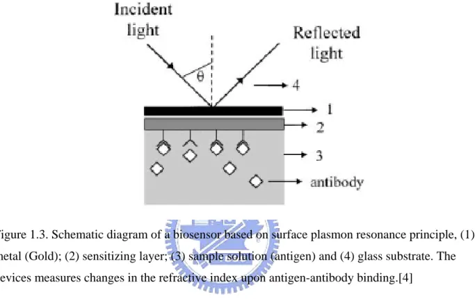
Another optical TIR-based biosensor that internal reflection in a light guide is SPR (surface plasmon resonance). SPR devices combine an evanescent wave detector with a biocomponent, generally, an antibody. The SPR method is a charge-density oscilation that may exist at the interface of two media with dielectric constants of opposite sign, for instance, a metal and a dielectric. An SPR optical sensor, generally, comprises an optical system, a transducing medium which interrelates the optical and (bio)chemical domains, and an electronic system supporting the optoelectronic components of the sensor and allowing data processing, energy carried by photons of light can be coupled or transferred to electrons in a metal. This coupling results in the creation of a plasmon, a group of excited electrons on the surface of the metal. The intensity of the plasmon is influenced by the type of metal and the environment of the metal surface. Changes in chemical properties within the range of the plasmon field (such as the protein interaction in antibody–antigen binding) cause changes in plasmon resonance. These changes can be measured as a change in the angle of incidence or shift in the wavelenght of light absorbed and can be measured as a change in the SPR signal (expressed in resonance units, RU). Most SPR instruments measure changes in the angle of incidence. A SPR-based biosensor specimen is tested for its adsorption to a covalently immobilized molecule by surface sensitive optical techniques. The amount of adsorption is measured as a function of time and results are generated in the form of a sensogram that shows the response units measured as a consequence of the adsorption (Homola, Yee, & Gauglitz, 1999) [13].
SPR biosensors are easy to use, label free, and can assay crude samples without purification (Homola et al., 1999) [14], but the whole SPR system is very expensive. Figure 1.3 shown an
Optical sensors make use of bioluminescent bacteria as Vibrio fischeri or Vibrio harveyi or chemiluminescent substances as luminol in combination with oxireductases for direct measurement. Optical luminescent biosensors have application in the control of fermentative processes, alcohol and in the determination of carbohydrates [15~18].
Figure 1.3. Schematic diagram of a biosensor based on surface plasmon resonance principle, (1) metal (Gold); (2) sensitizing layer; (3) sample solution (antigen) and (4) glass substrate. The devices measures changes in the refractive index upon antigen-antibody binding.[4]
Chemiluminescence occurs as a result of the oxidation of certain substances, usually with oxygen or hydrogen peroxide, producing visible light in the absence of any exciting illumination. The best known of these substances is luminal, shown in Figure 1.4. There are other more complex substance which will react in a similar way.
Figure 1.4. Reaction mode of luminal. [8]
The luminal is normally used as label. This can be employed in any assay involving oxygen, hydrogen peroxide or peroxidase. It is particularly useful with immunoassay. However, the sensitivity is limited because the quantum yield is only 1%. The most important advantage of chemiluminescence is that no external light source is need, the sensor can connect directly to the photodiode
A recent example pf a new type of chemiluminescence system involves adamantly dioxetine phosphate (Figure 1.4) which can be hydrolysed under the influence of alkaline phosphatase to form the adamantly dioxetine anion, which is unstable and fluoresces. The fluorescence lifetime is several minutes, unlike the more convectional type of luminescence, the structure of the materials involved and the mechanism of the fluorescence process are shown in Fig. 2.38. Such behavior could be used in many types of assay which involve phosphate ester hydrolysis using alkaline phosphatase. The adamant dioxetane phosphate could be allowed to compete with other organic phosphates for the phosphatase.
Field-effect transistors (FETs) are devices in which a transistor amplifier is adapted to be a miniature transducer for the detection and measurement of potentiometric signals, produced by a potentiometric sensor process on the gate of the FET. A separate reference electrode is also needed. Circuit wiring is minimized, so that in addition to miniaturization, electronic noise is greatly reduced and sensitivity is increased. The FET device can be part of an integrated- circuit system leading to the read-out, or to the processing of the analytical data.
1.2.5.1 Semiconductors - Introduction
Materials can be classified as metals, non-metals or semiconductors. Generally metals are good conductors of electricity, while non-metals are bad conductors i.e. they behave as insulators. Semiconductors come somewhere in between. The differences can be seen in the way that they form energy levels. Non-metal atoms form discrete bonding and anti-bonding molecular orbitals when they combine to form molecules. The bonding orbitals contain the bonding electrons while the anti-bonding orbitals are empty, unless electrons are promoted into these by excitation. The energy space between these levels is 'forbidden' and is therefore unoccupied. In metals, there are overlapping energy bands and so there is no forbidden region. Electrons can move freely throughout the bands, thus leading to their high conductivities. Semiconductors form energy bands, although in this case they are separated by a forbidden region. The lower band is known as the valence band (VB), while the upper band is called the conduction band (CB). The energy gap between the two is called the band gap. These features are shown in Figure 1.6.
Fig.1.6. (a) Classification of a material according to energy bands and interatomic spacing (b) The semiconductor band gap energy model. [20]
If small amounts of dopants are added to a semiconductor, it may acquire an excess of electrons to give a p-type semiconductor, or a deficit of electrons (excess of holes) giving an n-type semiconductor. Fifth-row elements (in the anodic Table), such as arsenic, form p-type semiconductors, while third-row elements, like gallium, will form n-type semiconductors.
The Fermi level (EF) is the point where the probability of filling the (energy) band is 0.5. For
same across the metal to the semiconductor. However when a potential is applied the levels on the two sides separate. The system then behaves like a capacitor and charges build up on each side. Figure 1.7 shows the energy levels across a p-type
Figure 1.7. Energy bands through an MIS system as a function of the applied voltage VG. [20].
semiconductor. It also shows the effect of applying a potential (a gate voltage, VG) across the
MIS system. With a small negative potential (VG < 0), there is an accumulation of electrons at the
metal/insulator (M/I) interface, and of holes (positive charges) at the semiconductor/insulator (S/I) interface. EF is shifted towards the VB lower than the value in the metal by an amount equal to
VG and the energy levels near the semiconductor become bent upwards to compensate for this.
With a small positive potential (VG > 0), there is a depletion effect as positive holes are repelled
from the S/I interface. In this case, the VB and CB bend downwards to compensate for this. If VG
equal. Now, the Fermi level is again midway between the VB and the CB - equivalent to the intrinsic level (Figure 1.7 (d)). Further increases in potential beyond the level lead to an excess electron concentration, thus causing the semiconductor to invert and become n-type in nature. The potential required to cause inversion is known as the threshold potential (VT).
1.2.5.2 Field- Effect Transistor
This is an arrangement to monitor and control changes in the MIS system. Inversion at a p-type S/I system can be monitored by two n-type sensors placed on either side of the p-type layer. The basic type of field-effect transistor (FET) is the insulated-gate FET (IGFET). This is shown in Figure 1.8. A source region (4), consisting of n-type silicon, is separated from a similar drain region (5), also of n-type silicon, by p-type silicon (1), with the insulator (2) consisting of silicon dioxide. The source is electrically biased with respect to the drain by the applied potential, VD. The gate (3) is a metal, insulated from the rest, so that it forms a capacitor sandwich, a
metal/insulator/semiconductor (MIS) arrangement as shown in Figure 1.9.
Figure 1.8. Schematic of the insulated-gate field-effect transistor (IGFET): 1, p-type silicon substrate; 2, insulator; 3, gate metal; 4, n-type source; 5, n-type drain; 6, metal contacts to source and drain. [19]
Figure 1.9. Schematic of the gate in an IGFET: M, metal; I, insulator; S, semiconductor. [19] This gate region is charged with a bias potential VG. The current from the drain (5) to the
source (4), ID, is measured. There is also a threshold potential, VT, at which silicon changes from
p-type to n-type, and inversion occurs. With a small positive VD and VG < VT, silicon (1) remains
in the p-state, and there is no drain current; n-Si is biased positive with respect to p-Si. When VG
> VT, there is surface inversion, and p-Si becomes n-Si. Now current can pass from drain source,
without crossing the reversed-bias p-n junction. VG now modulates the number of electrons from
the inversion layer and so controls the conductance. ID flows from source to drain, and is
proportional to both the electrical of the surface inversion layer and VD.
In order to convert this device into a sensor, the metal of the gate is replaced a chemically sensing surface. This general conformation is known as a CHEMFET and is shown in Figure 1.10.
In this arrangement, the chemically sensitive membrane (3) is in contact the analyte solution (7). A reference electrode (8) completes the circuit via the VG bias. The membrane potential
Figure 1.10 Schematic of a field-effect transistor with a chemically sensing gate surface (CHEMFET): 1, silicon substrate; 2, Insulator; 3, chemically sensitive membrane; 4, source; 5, drain; 6, insulating encapsulant; 7, analyte solution; 8, reference electrode. [19]
Scheme 1.1. Biocomponent and transducers employed in construction of biosensors.
Transducer Advantages Disadvantages Application Ion-selective electrode (ISE) Simple, reliable, easy to transport. Sluggish response, requires a stable reference electrode, susceptible to Amino acids, carbohydrates, alcohols and inorganic ions
FET
Absorption or emission of electromagnetic radiation Analyte(proteins, enzymes, antibody, antigens, sequence of DNA…)
Recognition element
(proteins, enzymes, antibody, antigens, sequence of DNA…) Diffusion of electroative or charged species Temperature change or heat release Mass and/or microviscosity alterations of wave propagation
Signal processing by dual or multiple channel ratio or subtraction followed by comparison to calibration
Electrochemical
Optical
Piezoelectric
Thermal
Chemical interaction induce potentiometric signal changeselectronic noise. Amperometric Simple, extensive
variety of redox reaction for construction of the biosensors, facility for miniaturize. Low sensitivity, multiple membranes or enzyme can be necessary for selectivity and adequate sensitivity. Glucose, galactose, lactate, sucrose, aspartame, acetic acid, glycerides, biological oxygen demand, cadaverine, histamine, etc.
FET Low cost, mass
production, stable output, requires very small amount of biological material, monitors several analytes simultaneously. Temperature sensitive, fabrication of different layer on the gate has not been perfected.
Carbohydrates, carboxylic acids, alcohols and herbicide
Optical Remote sensing, low cost, miniaturizable, multiple modes: absorbance, reflectance, fluorescence, extensive electromagnetic range can be used.
Interference from ambient light, requires high-energy sources, only applicable to a narrow concentration range, miniaturization can Carbohydrates, alcohols, pesticide, monitoringprocess, bacteria and others. . .
from optical interferences such as color and turbidity. the exception of when used in arrangement sucrose, alcohols, lipids, amines
Piezoelectric Fast response, simple, stable output, low cost of readout device, no special sample handling, good for gas analysis, possible to arrays sensors.
Low sensitivity in liquid, interference due to non specific binding. Carbohydrates, vitamins, pathogenic microorganisms (e.g. E. coli, Salmonella, Listeria, Enterobacter), contaminants (e.g. antibiotics, fungicides, pesticides), toxic recognition as bacterial toxins. Table 1.1. Types of transducers, their characteristics and application.
1.3 Motivation
For the era of minimization requirement of device, the scale of biosensor has become the micro-scale and reached the nano-scale. Because the specific site for immobilization is minimization, discover the ways to improve or amplify the signal is more and more important. The most immediate fashion is to produce more specific sites. The purpose of this thesis is to magnify the specific site for immobilization of bio-molecules.
Further, the selective immobilization of biomolecules onto silicon-based substrates at very high efficiency and reliability is the key to combining biological and electronic elements. In addition, the covalent and non-covalent bonding for capturing electronic signal from biosensor chip which made by semiconductor process are also important technique in the future.
molecule is reacted with sterptavidin (SA). The biotin–streptavidin interaction has a very high affinity and therefore represents one of the strongest non-covalent biological interactions. It is frequently used for labeling on various of biomolecules such as abtibody, lectins, sugars and nucleics, and has potential applications for biosensors and biosensing arrays. Thus the SA/biotin couple is useful as a molecular linker and has demonstrated extensive applications in biotechnologies such as immunoassays, purification[2,3], and pretargeted diagnosis and therapeutics[4].
1.4 Thesis Organization
This thesis is aimed to study the surface modification and immobilization reaction of biomolecules onto silicon surfaces and to amplify the immobilization site. A new kind of metal-semiconductor-metal (MSM) chip was proposed and used for chemiluminescence-type optical biosensor. The sensor is proposed to detect proteins which were widely used as the target molecule in the medical detection or biological studies. In order to setting up the experimental system, it requires lots of knowledge to accomplish this goal, including nanofabrication technology related to lithography procedures, self-assembly technique, biotechnology, organic chemistry, molecular biology, and electronics. In chapter 1, the general introduce of biosensors is described. Some experimental ideas and techniques from published literatures are cited and discussed in chapter 2. Chapter 3 briefly states the experimental reagents and experimental procedures for this research. In chapter 4, various solid supports were used to immobilize specific protein. We discuss the suitability of support and the activity of immobilized protein. We propose a novel protocol for immobilization and the MSM chip. The new chip is used to detect specific protein was also evaluated. At the last chapter, the conclusions of this thesis are given.
Chapter 2: Literatures Review
In this chapter, we will review some important literatures that relate to the thesis, These
literatures cover manipulation, creation and use of materials, devices and systems of
chemiluminnescence technology, immobilization technique and metal-semiconductor-metal
photo diode element which typically have dimension smaller than 100 nm. This is the key
spirit of nanotechnology. “There is plenty of room at the bottom,” as Nobel physicist Richard
Feynman pointed out more than 40 years ago [1]. Now we continue developing the room by
nanotechnology and the succeeding technology.
2.1 Principle of Chemiluminescence Type Biosensor
Based on the spectrum range of the optical biosensor techniques, the main applications at
visible wave band are fluorescence emission and chemilunescence (or bioluminescence). For
fluorescence, after absorption of light, the excited species will decay in one of a variety of
ways. However, while the excited molecule is undergoing radiationless decay, it may also
have time to react with other species, thus transferring its energy to new chemical species and
returning to the ground state with a diminished fluorescence output. This process is known as
“quenching”, this is a kind of energy transfer, leading the decrease of fluorescence, there are
several behaviors happen when fluorescence occurs (shown as Figure 2.1.1):
(1) S1 → S0 + hν (fluorescence)
(2) S1 → S0 (internal conversion)
(3) S1 → triplet states (i.e. T1) (intersystem crossing)
(4) S1 → fragments (dissociation)
(5) S1 + Q → products (quenching)
Chemiluminescence is another type of luminescence which processes low background
and high-intensity light output due to the catalyst of enzyme or other catalysts. In contrast,
discriminate the fluorescence signal. The characterization of fluorescence requires the
expensive instrument of fluorescence microscopy. Thus limits the sensitivity and the method
maybe more complex during the determination. However, chemiluminescence completely
eliminates these disadvantages. Chemiluminescence does not require the external light source,
and chemilunescence can be observed by the naked eye. Moreover, it provides real time
detection capability. Therefore, chemilunescence is an excellent way for biochemical
detection. Figure 2.1 shows the diagram of fluorescence (a) and chemilunescence (b);it is
obvious at figure 2.1 (a) that fluorescence method needs external light for excitation,
chemluminescence is a spontaneous reaction with the emission of light. Ttable 2.1
summarizes the comparison of fluorescence and chemiluminescence method.
Fluorescence Chemiluminescence Advantages z Sensitive z Variety of fluorescence-conjugated biomolecules available z No unwanted background luminescence
Disadvantages z Suffering from external light interference
z Low photochemical stability
z Expensive read out system
z Limited by the availability of chemiluminescent probes
Table 2.1. The comparison between fluorescence and chemiluminescence method.
2.1.1 Introduction of Luminol
Luminol is a versatile chemical that exhibits chemiluminescence, with a striking blue
glow, when mixed with an appropriate oxidizing agent. It is a white to slightly yellow
crystalline solid that is soluble in water and most polar organic solvents.[2]
Luminol is usually used by forensic investigators to detect trace amounts of blood left at
crime scenes. It is also used by biologists in cellular assays for the detection of copper, iron,
and cyanides. To exhibit its luminescence, the luminol must first be activated with an oxidant.
Usually, a solution of hydrogen peroxide (H2O2) and a hydroxide salt in water is used as the
activator. In the presence of a catalyst such as an iron compound, the hydrogen peroxide is
decomposed to form oxygen and water. Figure 2.2(a) demonstrates the typical chemical
Figure 2.2. (a)The typical reaction of luminol. [3]; (b) the detailed reaction steps of luminol
catalyzed by HRP.
(a)
as a label is that, in presence of a small amount of enhancers, the intensity of the light
emission is increased by several orders of magnitude and background light emission from the
luminol-peroxide reagent is great reduces, which leads to a dramatic increase in the signal.
Luminol is a known substrate, and is used to measure the activity of enzyme [4]. The detailed
reaction of HRP enzyme on the luminol molecule us illustrated in figure 2.2 (b).
Detection by chemiluminescence has now become the main method of choice for fast and
sensitive assays of enzyme conjugates on blots. While phosphate-containing dioxetane
compounds are widely used as the chemiluminescent substrates for alkaline phosphatase
conjugates, the compound luminol and its derivatives (diacylhydrazides) are the
chemiluminescent substrates of choice for horse radish peroxidase (HRP) conjugates. HRP
catalyzes the oxidation of luminol in the presence of hydrogen peroxide, during which an
excited intermediate is formed and subsequently decays to the ground state by emitting
2.2 Immobilization Technique
A major advance in materials fabrication technology during the last 10 years has been the development for self-assembly methods [6]. Self assembled monolayers (SAMs) provide well defined structures and chemistries that can be systematically varied. Also, spatially defined arrays of SAMs can be prepared by combining self-assembly with patterning methods such as microcontact printing or photolithography [7]. In addition, SAMs can be used to immobilize peptides, proteins, and other biomolecules to the surface of interest to prepare the complex surfaces required for well-defined biological experiments. A surface skill used in nature with elegance and precision is the ability to order and organize complex molecules at surfaces. Precision immobilization typically aims to copy nature’s way of organizing molecules and is thus an example of a biomimetic strategy. Possibilities for surface immobilization of biomolecules are suggested in Table 2.1. The characteristics of successful precision engineered biorecognition surfaces include the presence of one receptor site, an appropriate surface density of those sites, controlled orientation of the sites, some molecular mobility to enhance ‘‘docking,’’ and stability (of the biomolecular conformation and the film integrity). The ability to inhibit non-specific reactions (in particular, protein adsorption) is also essential to succeed at emulating nature’s surface signal delivery strategy.
The scientific roots of this area of surface molecule immbilization lie in the Langmuir–Blodgett deposition of lipids and surfactants [9]. The discovery in 1983 of thiol assembly on gold [10] launched an explosion of publications and new discoveries for self-assembling. Self-assembly of complex organic structures on solid surfaces has been observed for phospholipids [11], silanes [12], n-alkyl thiols [20, 13, 14], porphyrins [15], nucleotide bases [16], hydrocarbons [17], proteins [18], and many other organic structures. The choice of a suitable immobilization method is mainly determined by the chemical and physicochemical properties of the immobilization support and of the compound to be immobilized. The adsorption of compounds onto a surface is the simplest immobilization method. It is based on the interactions between local dipoles existing on the interacting molecules. The polarity of the molecule can be stationary due to polar groups, of which –OH, –NH2, –C=O, NH-groups are of particular importance, as they form strong
hydrogen bonds. Most frequently biomolecules are bound covalently to the immobilization support through amino groups, which are accessible on the exposed areas of the biomolecules. They react readily with aldehyde and epoxide groups and with carboxylic or amino groups after activation by carbodiimide- or succinimide-derivatives. Taking protein as an example, after deposition of the protein solution, an incubation step at room temperature in a humid chamber is sufficient for efficient protein immobilization. This makes these procedures compatible with the fabrication of semiconductor devices. Silanisation is the most common procedure for the chemical modification of glass surfaces. Amino groups are introduced by aminopropyltriethoxy- (or trimethoxy) silane. Epoxide groups are introduced via 3-glycidoxypropyltrimethoxysilane. Treatment with periodic acid leads to their oxidation to aldehyde groups. Surfaces with aldehyde or epoxide groups sometimes show reduced background signals, as no unspecific electrostatic interactions are possible, whereas aminofunctionalized surfaces are usually positively charged leading to the unspecific adsorption of negatively charged proteins [19]. Carboxylic groups are present on the surface
of carbonaceous electrodes or are generated on the surface of gold layers by self-assembling of thiol compounds, such as 11-mercaptoundecanoic acid [20]. These groups have to be activated to allow covalent coupling of proteins, which is done by incubation with a carbodiimide, such as 1-ethyl-3-(3-dimethylaminopropyl) carbodiimide hydrochloride (EDC) in the presence of N-hydroxysuccinimide (NHS). Proteins with an extremely high affinity for biotin are avidin and streptavidin (dissociation constants of approx. 10−15M). Due to the four
biotin-binding sites on each protein molecule a layered structure can be built with a biotinylated surface, a biotin binding protein in the second layer and the 16 biotinylated capture protein [19]. Protein-sensing devices are of increasing importance in the fields of diagnosis, monitoring systems or biological research, as it is realized that proteins are one of the active compounds in organisms. Thus their concentrations, covalent modifications, localizations and activities within or outside cells, tissues or organisms reflect reactions of the organism to its surroundings, which may be indicative of diseased states, toxic or other adverse effects or for contamination with biohazards, such as microbial toxins.
2.2.1 Cleland’s reagent: DTT
Dithiothreitol (DTT) is a Cleland’s reagent; the reducing potential of this versatile reagent was first described by Cleland in 1964. Due to their low redox potential (-0.33V) they are able to reduce virtually all accessible biological disulfides and maintain free thiols in solution despite the presence of oxygen. The compounds are fully water-soluble with very little of the offensive odor of the 2-mercaptoethanol they were meant to replace. Since Cleland’s original report, literally hundreds of references have appeared citing the use of mainly DTT for the reduction of cystine and other forms of disulfides.
disulfide bonds in a two-step reaction that involves the formation of a mixed disulfide (Scheme 2.1 and Scheme 2.2). In the second stage of the reducing process, the mixed disulfide is cleaned by anther molecular of reductant, freeing the sulfhydryl and forming a dimer of the reducing agent through the formation of a intermolecular disulfide exchange is nearly equivalent for the reguctant and target protein. Thus, monothiol compounds are usually require in extreme excess to drive the reaction to completion [21].
Scheme 2.1. Thiol-containing disulfide reductants reduce disulfide groups through a multistep precess preducing a mixed intermediate [21].
The presence of two sulfhydryl group in DTT, however, allows the formation of a favored cyclic disulfide during the course of target protein reduction (Scheme 2.2) This drives the equilibrium toward the reduction of target disulfides. Therefore, complete reduction is possible with much lower concentrations of DTT than when using monothiol systems.
Scheme 2.2. DTT is highly efficient at reducing disulfides, since a single molecule can reduce the intermediate mixed disulfide by forming a ring structure [21].
2.2.2 The Effect of Li as a Chelating Agent on the Ring Opening of Cyclitol
Epoxides
Over the last years, aminocyclitols have gained interest as pharmacological tools for the study of cellular processes linked to the inositol phosphate cycle, as well as potential glycosidase inhibitors [22, 23]. The regio- and stereoselective synthesis of aminocyclitol is more and more interesting [24]. Pedro Serrano et. al have demonstrated a useful ring opening process for epoxides (in Scheme 2.3)
which the benzyloxy group adopts an axial disposition to enable intramolecular metal chelation with the epoxide. Li salts behave similarly to promote epoxide opening through an intramolecular chelation process. The Scheme 2.4 and Scheme 2.5 semonstrate the main reaction flow of ring opening reaction for epoxides.
Scheme 2.4. Lithium promoted opening of cyclitol epoxides 1 (R=H) and 2 (R=Bn). [26]
Scheme 2.5. Synthesis of cyclitol analogues by regioselective C1 opening of the starting epoxide. [27]
2.4 Fundamentals of the MSM-PD
The MSM-PD is a planar device, and it consists of two back-to-back connected Schottky diodes on a semiconductor layer. The metal structure is composed of two contact pads and interdigitated lines, which form the active area of the device. The device works by absorbing optical energy and converting incident photons into a time-varying electrical signal. When the active area of the device is illuminated, carriers in the semiconductor absorption layer (also known as electron-hole pairs) are generated by incident photons having energy greater than the bandgap energy (Eg).
The carriers are transported to the metal contact pads, and a current is detected in the external circuit under the application of an external bias voltage. Figure 2.3 shows the cross section of the MSM-PD, signifying the dimensions, carrier motion, and the electric field orientation. S and W refer to the electrode spacing and width, respectively, d to the thickness of the active area, and E to the electric field.
metal contacts to uniform-doping n-type semiconductor. The charge distribution, electric-field distribution, and energy-band diagrams in this device with a small positive bias voltage are shown in Figure. 2.4 (b), (c), (d), respectively [28]. As a small positive bias voltage is applied, one side is forward-biased and the other one is reverse-biased. The W1 and W2 denote the depletion widths at the forward and reverse biase Schottky junctions in the n-type semiconductor, respectively.
2.2.1 Current Transport Mechanism
Figure 2.5 Current transport mechanism under forward bias
The current transport in metal-semiconductor contacts is primarily due to majority carriers. The four basic transport processes for a Schottky diode [29, 30, 31] are shown in Figure 2.5 under forward bias conditions (the inverse processes occur under reverse bias):
(1) Emission of electrons from the semiconductor over the top of the potential barrier into the metal
(2) Quantum mechanical tunneling of electrons through the barrier (3) Recombination in the space-charge region
(4) Recombination in the neutral region (also hole injection from the metal to the semiconductor)
Condition (1) and (2) are dominant for moderately doped semiconductor, and heavily doped semiconductors, respectively. Diffusion [32, 33], thermionic emission[34], and combined thermionic emission diffusion[35, 36] theories are used to study the emission of electrons over the barrier. The thermionic emission theory
applicable to high-mobility semiconductors; and for low mobility semiconductors the transport is described by the diffusion theory.
2.3 Characteristic parameters of MSM-PD 2.3.1 Quantum efficiency
Quantum efficiency, η (0 ≤η≤ 1) of a photodetector is defined as the number of carriers (electron-hole pairs) collected to produce the photo current (Iph) generated per
the number of incident photons. The equation of external quantum efficiency (η) is given by
ν
η
/h
P
/q
I
in ph=
Where q is magnitude of the electronic charge, h is Plank constant, ν is the frequency of incident light.
2.3.2 Responsivity
Responsivity of the detector is the ratio of the photo current flowing in the detector to the incident optical power:
(A/W)
1.24
P
I
R
in ph=
ηλ
=
Where λ is the wavelength of incident light.
2.3.3 Response time
The response-time limit of all photodetectors is determined by basically three effects: the time of carrier diffusion to the junction depletion region, τ0; the transit
Chapter 3: Experiments
3.1 Reagents and Instruments
All the experiments were proceeded at either National Chiao Tung University (NCTU)
or National Nano Device Laboratories (NDL). All the equipments were also conducted in our
laboratories in NCTU. The reagents were purchased commercially and used by following with
the directions unless specially mentioned. All the reagents were listed alphabetically in the
form of “Name {abbreviation; chemical formula; purity; manufacturer}”. Some information
will be omitted if not available or not necessary. The following text will use the abbreviation
of the reagent.
3.1.1 Reagents
3-aminopropyltriethoxysilane {APTES; H2N(CH2)3Si(OC2H5)3; 97% purity; Sigma}
APTES was used to modify the property of the SiO2 surface. The ethoxy functional groups of
APTES were displaced through formation of covalent bond between the hydrophilic hydroxyl
groups of the SiO2 surface and the silicon atom in APTES molecule. This process leads to the
formation of a molecular layer of amino groups for futher bonding with biochemical
materials.
Acetone {CH3COCH3; ≥ 99.5% purity; Sigma}
Acetone was used to remove the excess and unnecessary chemical reagent or particles.
Toluene {C6H5CH3; ≥ 99.5% purity, anhydrous; Sigma}
Toluene was diluted with DI water to provide an environment that facilitates the APTES
Bovine serum albumin {BSA; for molecular biology, powder}
Bovine serum albumin consists approximately 50% of the total protein in serum. It is a
non-acetylated protein served as a blocking agent.
Deionized and distilled water {DI water, ddH2O}
The water we used was purified with filters, reverse osmosis, and deionized system to the
resistance more than 18 MΩ‧cm. DI water was used to clean, wash, and as a solvent.
N,N-Dimethylformamide {DMF; HCON(CH3)2; for molecular biology, ≥99% ; Sigma}
It was a solvent for dissolving many hydrophobic organic compounds like rhodamine in the
experiments.
Hydrogen chloride {HCl; ≥99% purity; Sigma}
1 M HCl in DI water was used for pH adjustment.
Hydrogen peroxide {H2O2; ≥30% purity; Sigma}
Hydrogen peroxide was mixed with sulfuric acid to form piranha solution which cleaned the
wafer surface.
Phosphate-buffered saline tablets {PBS, 1X; CALBIOCHEM}
PBS, a biological buffer solution, was used to increase the selectivity of the DNA chips by
washing away any non-hybridized nucleic acids. This chemical is dissolved in one liter
aldehyde. It was very light-sensitive and must be stored at 4℃. During the processing, it mustkeep from light with aluminum foil.
Sodium chloride {NaCl; ≥ 99.5%; Sigma}
Sodium chloride was used to prepare SSC or other biological buffer.
Sodium hydroxide {NaOH; 98% purity; Sigma}
10 M Sodium hydroxide in DI water was used to adjust the pH.
Sodium phosphate dibasic dihydrate {NaH2PO4; ≥99.5%; Riedel-deHaën}
Sodium phosphate solution was a widely used biological buffer. This chemical was also a
family of PBS.
Sulfuric acid {H2SO4; 98% purity; Sigma}
Sulfuric acid was mixed with hydrogen peroxide in a 3:1 ratio to remove impurities on the
surface of the wafer or devices. This material was very corrosive and dangerous. We must
handle it with carefulliness and patience.
Tween 20 {Polyethylene glycol sorbitan monolaurate; Sigma}
Tween 20 was a non-ionic detergent to control the stringency of hybridization.
Cysteamine { NH2 CH 2 CH 2SH; ~95%; Sigma}
Cysteamine was used for chemical modification.
DDT (Dithiothreitol) { C4 H 12 O 2S2; >99%; DUCHEFA BIOCHEMIE}
Sulfo-NHS-Biotin { C14H18O8N3S2Na; 443.43; Pierce}
The reagent is used for labeling surface functional groups and biologically active molecules
such as antibodies, lectins sugars, nucleic acids or molecules with free amino group. Stored
under 4℃ .
Streptavidin−FITC from Streptomyces avidinii {essentially salt-free, lyophilized powder, ≥ 5 units/ mg protein; Sigma}
This protein had a high affinity for biotin. Prior to use, the powder needed to dissolve in the
PBS. It must be stored under -20℃ .
Streptavidin-HRP { Streptavidin−Peroxidase from Streptomyces avidinii; 443.43; Sigma}
This protein exhibited high affinity with biotin. The powder needs to dissolve in PBS buffer
prior to use. Stored under -20℃
Luminol {from Chemiluminescent Peroxidase Substrate; Sigma}
The kit for chemiluminescence was consisted with luminol and H2O2.
Conduritol B epoxide {1,2-Anhydro-myo-inositol; 155.68, Sigma}
This reagent is used for surface immobilization.
Fluorescence Microscopy
Olympus BX21 with microscope digital camera of DP71.
Image Analysis Software
Image-Pro Plus Version 6.0, Media Cybernetics Inc.
UV-Visible Spectrophotometer
SHIMADZU, UV-1601
Semiconductor Parameter Analyzer
3.2 Procedures
The deionized water (DI water) with 18 MΩ-cm was used in the thesis. A thermal oxide layer was grown on <100> silicon wafers by heating to 900℃ for 3 hours.
3.2.1 Self-assembly of B-epoxide on APTES for enhancing immobilization
efficiency of streptavidin
z Step 1: Cleaning the silicon wafer with piranha solution. Prior to any functionalization, the
chip surface was cleaned in piranha solution (H2SO4 : H2O2 = 7 : 3) for 1 hour. To prepare
the piranha solution, first pouring H2SO4 and then adding H2O2, check the temperature to
avoid too much increase since it will extreme hot and dangerous.
z Step 2: The slides are then washed thoroughly with DI water and then dry the slides by
flushing nitrogen. After that, soaked slides with 10% APTES in dried toluene for 30 minutes at room temperature.
z Step 3: Preparing the 10mM B epoxide solution (solvent: H2O), adding equal volume of
LiClO4 solution with concentration of 20mM.
z Step 4: Removal of the solution of APTES, the microchips were rinsed several times with
toluene and acetone and dried in an oven at 120 °C for 1 hour.
z Step 5: Removing the slides away the oven, waiting a moment until the temperature of
slides return to room temperature. Soaking the slides with LiClO4 solution at 70 °C for 12
hours.
z Step 6: Removing the slides and rinsing with DI water, then soaking the slides with 5mM
sulfo NHS-biotin (solvent: DMSO) for 6 hours.
z Step 9: Removing the slides and rinsing with PBS buffer solution, then soaking with
streptavidin-FITC solution (0.01mg streptavidin-FITC with 10ml PBS buffer) for 2hours.
Scheme 3.1. The procedures for the of immobilization of biotin with streptavidin.
3.2.2 Self-assembling of cysteamine on GNPs for enhancing the
immobilization efficiency of streptavidin
z Step 1: Cleaning the silicon wafer with piranha solution. Prior to any functionalization, the
the piranha solution first, pouring H2SO4 and then adding H2O2, check the temperature to
avoid too much increase since it will extreme hot and dangerous.
z Step 2: The slides are then washed thoroughly with DI water and then dry the slides by
flushing nitrogen. After that, soaked slides with 10% APTES in dried toluene for 30 minutes at room temperature.
z Step 3: Removial of the solution of APTES, the microchips were rinsed several times with
toluene and acetone and dried in an oven at 120 °C for 1 hour.
z Step 4: Removing the slides away the oven, waiting a moment until the temperature of
slides return to room temperature. Soaking slides with GNPs solution at RT for 30 minutes, slides are then washed with deionised water.
z Step 5: Then preparing the cysteamine solution, 10ml deionised water with 0.0154g
cysteamine and 0.0154g DDT, after thoroughly mixing and dissolving, GNPs-APTES-modified slides were dipped into this solution for 3 hours.
z Step 6: Removing the slides and rinsing with DI water, then soaking the slides with 5mM
sulfo NHS-biotin (solvent: DMSO) for 6 hours.
z Step 7: Removing the slides and rinsing with PBS buffer solution, then soaking with
streptavidin-FITC solution (0.01mg streptavidin-FITC with 10ml PBS buffer) for 2hours, steptavidin-FITC can be substituted by streptavidin or streptavidin-HRP.
Scheme 3.2. The procedures for the immobilization of biotin with streptavidin by the assistingn of GNPs and cysteamine
3.2.3 Chemiluminescence type photo-sensor from luminol reaction of
HRP-catalyst
In this part, we fabricated MSM (metal-semiconductor-metal) chip by a serie of semiconductor processes, then we self-assembled and immobilized several molecules onto the surface of MSM chip. Finally, we poured the substrate of chemiluminescence into the system and recorded captured the electronic signal by precision instrument.
3.2.3.1 MSM Biosensor Manufacturing
Single-crystalline N-type <1 0 0> silicon wafers (resistance: 2~7Ω-cm) were used through all the experiments.
The detailed processes of Metal-Semiconductor-Metal Photodetector are listed below. Fabrication process :
z Step 1: Standard cleaning [48] the silicon wafer. Firstly, using the DHF to remove the
native oxide on the silicon surface. Secondly, rinsing the wafers in SC-1 solution to remove particles and some organic compounds, then rinsing the wafers in SC-2 solution to remove alkaline metallic ions and alkaline-earth metallic ions. Since H2O2 was added in
SC-1 and SC-2 to improve the activity of the chemical, the oxidative activation of H2O2
will result in the formation of native oxide. Finally, rinsing the wafers in DHF solution to remove the native oxide film.
z Step 2: Send the wafers into low pressure furnace tube to grow 2000 Å thermal oxide. z Step 3: Spin coating E-beam positive photoresist on the wafers.
z Step 4: Using E-beam lithography (Leica WePrint 200) to write the zero mask pattern on
the wafers. (The zero-mask is served as alignment calibration.) the wafers were developed in TRACK (TEL CLEAN TRACK MK-8) system. 2.38% tetramethyl ammonium hydroxide (TMAH) solution was used for the development.
z Step 5: Etching away the oxide layer by reactive-ion-etching (RIE) [49] (TEL5000).
z Step 6: Removing the photoresist by OZONE plasma (FUSION OZONE ASHER) and
then rinsing in SPM solution ( H2SO4 : H2O2 = 3 : 1, 120oC). Then immersion in SC-1 to
remove side-wall polymers formed during step 5.
lithography.
z Step 10: Etching away dry oxide layer by TEL5000. Then rinsing in SC-1 to remove
side-wall polymer.
z Step 11: Removing photoresist by OZONE and SPM.
z Step 12: Spin coating photoresist and then patterning interdigitated lines by E-beam
lithography. Develop by TRACK system.
z Step 13: Using TCP to etch away the single crystalline silicon and ensuring the better
adhesion and contact of metal lines with the silicon surface.
z Step 14: Depositing metals by thermal coater (Cr,Au) or Electron-Gun (Cr,Pt). z Step 15: Using lift-off techniques to remove the unwanted metal.
z Step 16: Depositing oxide passivation layer by PECVD. The thickness is 760Å.
z Step 17: Spin coating E-beam photoresist then E-beam lithography to form the pattern of
probe contacts. Then, development by TRACK and etch away by BOE (Buffered oxide etching solution NF4 : HF = 5:1) The device is completely finished here.
Scheme 3.3. Process flow chart of MSM-PD fabrication. Zero mask Pad oxide Active window Interdigitated lines Metal deposition Lift-off techniques Anti-reflection oxide
3.2.3.2 Immobilization of Biomolecules onto the Surface on MSM Biosensor
z Step 1: Cleaning the silicon wafer with piranha solution. Prior to any functionalization, the
chip surface was cleaned in piranha solution (H2SO4 : H2O2 = 7 : 3) for 1 hour. To prepare
the piranha solution first, pour H2SO4 and then adding H2O2, check the temperature to
avoid too much increace since it will extremely hot and dangerous.
z Step 2: The slides are then washed thoroughly with DI water and then dry the slides by
flushing nitrogen. After that, soaked slides with 10% APTES in dried toluene for 30 minutes at room temperature.
z Step 3: Removal of the solution of APTES, the microchips were rinsed several times with
toluene and acetone and dried in an oven at 120 °C for 1 hour.
z Step 4: Removing the slides away the oven, waiting a moment until the temperature of
slides return to room temperature.
z Step 5: Removing the slides and rinsing with DI water, then soaking the slides with 5mM
sulfo NHS-biotin (solvent: DMSO) for 6 hours.
z Step 6: Removing the slides and rinsing with PBS buffer solution, then immersion with
Chapter 4: Results and Discussion
We studied the suitable molecules for immobilization and metal nonoparticles on silicon dioxide surface. By utilizing semiconductor process, we immobilized appropriate molecules on selected area of pattern surface with self-assembling technique. After that, we successfully immobilized GNPs (gold nanoparticles) on the selected area. Furthermore, we also grafted the other molecules onto GNPs. By following this protocol procedure, we had attached a couple of biomolecules. We evaluated the immobilization efficiency with SEM, fluorescence microscopy, UV-visible spectrophotometer and IV characteristics.
4.1 Optimization of Self-assembly Parameters on Silicon Oxide Surface
The contact angle is the angle at which an equilibrium is reached between solid, liquid and gas phases. The contact angle is specific for any given system and is determined by the interactions across the three interfaces. This technique is usually performed with a small liquid droplet resting on a flat horizontal solid surface. The shape of the droplet can be determined by the Young-Laplace equation. The contact angle plays the role of a boundary condition. Contact angle is measured by a contact angle goniometer. The contact angle is not limited to a liquid/vapor interface; it can be also applied to the interface of two liquids phases or two vapors analogues. In this study, we use DI-water as liquid phase. Figure 4.1(a) depicts the image of contact angle. The image is obtained for the sample after cleaning with piranha solution. The water profile on the slide is not like a drop, indicating that the free energy of surface is rather high. Hence, the surface exhibits high capability of chemical reaction. Figure 4.1(b) is the image for the surface immobilized with APTES. The contact angle is increased.
Scheme 4.1 The process flow for self-assembly.
Figure 4.1. Images of contact angle: (a) after cleaning with piranha solution and (b) after APTES process.
![Figure 1.1. Schematic of a typical thermoresistor device is used as a biosensor in enzymatic reactions.[8]](https://thumb-ap.123doks.com/thumbv2/9libinfo/8411762.179880/16.918.128.604.105.453/figure-schematic-typical-thermoresistor-device-biosensor-enzymatic-reactions.webp)
![Figure 1.2. Schematic diagram of a typical QCM.[11]](https://thumb-ap.123doks.com/thumbv2/9libinfo/8411762.179880/17.918.225.652.139.477/figure-schematic-diagram-typical-qcm.webp)
![Figure 1.4. Reaction mode of luminal. [8]](https://thumb-ap.123doks.com/thumbv2/9libinfo/8411762.179880/20.918.118.834.338.938/figure-reaction-mode-of-luminal.webp)


![Figure 2.2. (a)The typical reaction of luminol. [3]; (b) the detailed reaction steps of luminol catalyzed by HRP](https://thumb-ap.123doks.com/thumbv2/9libinfo/8411762.179880/34.892.130.755.116.902/figure-typical-reaction-luminol-detailed-reaction-luminol-catalyzed.webp)
