行政院國家科學委員會專題研究計畫 成果報告
奈米碳管功率放大器研究
計畫類別: 個別型計畫 計畫編號: NSC94-2623-7-009-001- 執行期間: 94 年 01 月 01 日至 94 年 12 月 31 日 執行單位: 國立交通大學光電工程學系(所) 計畫主持人: 戴亞翔 共同主持人: 鄭晃忠 報告類型: 完整報告 處理方式: 本計畫可公開查詢中 華 民 國 95 年 1 月 18 日
行政院國家科學委員會專題研究計畫成果報告
奈米碳管功率放大器研究
The Research of Carbon Nanotubes-Based Power Amplifier
計畫編號:NSC 94-2623-7-009-001 執行期限:94 年 1 月 1 日 至 94 年 12 月 31 日 主持人:戴亞翔 助理教授 國立交通大學光電工程學系 共同主持人:鄭晃忠 教授 國立交通大學電子工程系 中文摘要 近年來隨著奈米材料以及奈米科技的研發, 許多傳統的技術或產品都嘗試著用新研發出 的奈米材料來改善其原本的特性,而在真空 微電子元件方面也因1991 年 Iijima 等人在實 驗的過程中發現奈米碳管的存在而有了新的 發展。在1904 年,英國科學家佛來明研發出 可以控制電流訊號的電子元件「佛來明二極 體」(Fleming Diode),在 1907 年至 1960 年間, 真空管的技術持續發展,且在1950 年至 1960 年間研發出大部分類型的真空管,其中包含 了三極 結構的真空 管。在電晶 體研發成功 後,半導體元件大幅地取代了真空管元件, 一直到近年來結合半導體製程而有真空微電 子元件的研發,奈米碳管被利用於真空高功 率與高頻功率放大器之中,因為奈米碳管具 有強的機械性質、不活潑的化學性質、低的 功函數以及較大的高寬比,被視為最適合做 為電子 束場發射源 的材料之一 ,在本實驗 中,我 們結合既有 的三極結構 以及奈米碳 管,嘗試藉由改變元件的結構以得到較高的 操作頻率。我們藉由增加閘極下絕緣層的厚 度以及光阻/鋁/光阻的結構以達到抵抗活性 離子蝕刻與去除非場發射區催化金屬,在實 驗結果中我們發現藉由此結構亦能有效抑制 閘極與陰極之間的漏電流。 Abstract
With the development of nano-technologies these years, many researching groups use these new nano-materials to improve the performance of conventional products. Since the observation of carbon nanotubes by Iijima in 1991, there were some further improvements in vacuum electronics. In 1904, British scientist John Ambrose Fleming first showed his device to convert an alternating current signal into direct current. It is so called "Fleming diode". From 1907 to 1960, the vacuum tubes kept on developing and almost all kinds of vacuum tubes which include the triode structure were invested from 1950 to 1960. After the investment of transistor, a large part of vacuum tubes were replaced by bipolar transistors or MOS transistors. Resulting from the import of semiconductor processes, the development of vacuum micro-electronics became an important
field recently. Because of the high mechanical properties, inert chemical properties, low work-function, and high aspect ratio, carbon nanotubes is one of the most promising materials as the emitters in the field emission device. In our experiment, we use carbon nanotubes in the triode structure and try to increase the operating frequency by increasing the thickness of insulator under the gate electrode. We also use
the structure photoresistance/Al/photoresistance to
protect the devices from the etching of RIE and remove catalyst metal from unwanted area. Besides, we found that this device structure can suppress the leakage current from cathode to gate electrode.
Introduction
High frequency power microwave amplifiers have been a subject of research for number of years [1-2]. High power density of devices is characterized in the form of both drive electron beam and output power. A high current density and high operating frequency are needed in a typical power microwave amplifier. For a conventional thermionic cathode generally can not reach such current density and there are some problems of noise which resulting from the heating on emitters. Hence many research groups try to design a new structure, such as Spindt type [3] silicon tips, or find some new materials with small or negative work function, such as diamond [4], diamond-like carbon [5], and carbon nanotubes [6-8] to make a electron emitter without heater.
Since the observation of carbon nanotubes in 1991 by Iijima [9], it has been recognized as a very potential material in many applications. One of the most promising applications is to be used as emitters in field emission devices. Due to strong mechanical properties, inert chemical properties,
negative work function, and high aspect ratio, carbon nanotubes are expected that it can gain a very high emission current density with relative low electric field as compare with conventional silicon tips. There are many methods to synthesize carbon nanotubes, however, thermal-CVD at high temperature (>750 °C) [10] is one of the most possible way to fabricate a power amplifier device with high current density and selective growth of carbon nanotubes. Compare with the method of printing, it can gain better adhesion between carbon nanotubes and the substrate which make it possible to operate the devices at higher electric field.
In our experiment, we use carbon nanotubes as the emitters in the triode structure [11] to improve the emission current density. Than we increase the thickness of insulator under gate electrode to decrease the capacitance between gate and the substrate. Here we use a PR/Al/PR structure to protect the devices from the etching of RIE (reactive ion etcher) and remove catalyst metal (Fe) from unwanted area by ultra-sonic in ACE. From the results of emission current measurement, we found that leakage current between cathode and gate can also suppressed with thicker insulating layer.
Experiment Processes
First, we formed a 1 um thermal oxide on n-type (100) silicon wafer with low
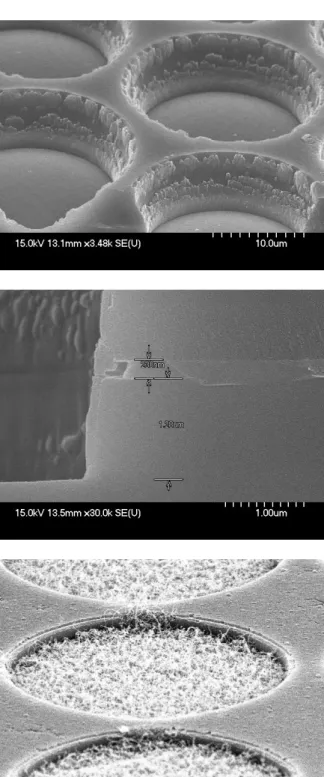
resistance (1-10 Ω/cm2). A poly silicon layer (200 nm) was deposited by LP-CVD as the gate electrode on the insulating layer. We used the method of lithography to define the pattern. After that, RIE was used to etch poly-Si and thermal oxide than we used E-beam evaporation to deposit 5 nm Fe on the wafer. We remove the catalyst metal on PR by lift-off in ACE. Finally, we grow carbon nanotubes in a thermal-CVD in C2H4/N2/H2 (5/1000/400 sccm) mixed gases at 700 °C for 20 min. The flow chart of processes is shown in Fig. 1 and the SEM image of the triode structure is shown in Fig. 2.
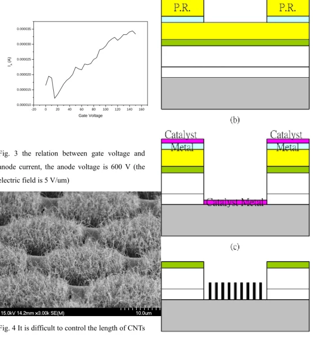
After the fabrication of devices, we measured the emission current density in a vacuum chamber at 5x10⁻⁶ torr with Keithley 237 high voltage SMU. The curve of IA-VG is shown in Fig. 3. In the measurement, we found that the leakage current between cathode and gate is very high for large part of samples and the anode current decrease with the increase of gate voltage. In the SEM image in Fig. 4, the length of carbon nanotubes is over the height of insulating layer plus gate and it may cause a short circuit between cathode and gate. As the gate voltage increase, a lot of electrons will be attracted to the gate which results in the drop of emission current.
To protect the device under the RIE process (because the PR can not hold for a very long time if the thickness of insulating layer is too large) and achieve
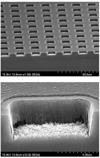
the lift-off process with a very thick insulating oxide layer, we used a PR/Al/PR layers on poly-Si gate. We defined the pattern on the first PR layer than used RIE to etch Al. After that, we used RIE to remove the first PR layer and etch the second PR layer. We used Al layer as a hard mask to etch poly gate and 3-um insulating oxide (1 um thermal oxide plus 2 um PE-CVD oxide). Continually, we deposited catalyst metal (Fe) be E-beam evaporation and remove PR/Al by lift-off by ultra-sonic in ACE. The flow chart of processes is shown in Fig. 5. With thicker insulating oxide layer, the capacitance between cathode and gate, Cg, is greatly decreased (1/3 of original capacitance, C=ε/d) and the operating frequency can be largely improved (resulting from the suppression of RC delay). Theoretically, we can gain a power amplifier with higher operating frequency. The image of SEM is shown in Fig. 6. From the data of measurement, the leakage current between cathode and gate was also suppressed from mA to uA.
Conclusions
In this paper, we proposed a novel structure, PR/Al/PR layers, to make very thick of insulating oxide layer possible. With carbon nanotubes as emitters and a very thick insulating layer between cathode and gate, we can make a power amplifier with high emission current density and high operating frequency. It
can also suppress the leakage from gate to cathode results from the short circuit by over-long carbon nanotubes.
Reference
[1] J. Benford, J. Swegle, and E. Schamiloglu, “High Power Microwaves, 2nd ed. Bristol, UK: IOP, 1992”.
[2] R. J. Baker and E. Schamiloglu, Eds., “High Power Microwave Source and Technologies, Piscataway, NJ: IEEE, 2001.”
[3] Talin, A. A., Dean, K. A., and Jaskie, J. E., “Field emission displays: a critical review,” Solid State Electronics, Vol. 46, pp963-976, 2001
[4] Köck, F.A.M., Garguilo, J.M., and Nemanich, R.J., “Imaging electron emission from diamond film surfaces: N-doped diamond vs. nanostructured diamond,” Diamond and Related Materials, Volume: 10, pp. 1714-1718, 2001
[5] Debski, Tomasz; Barth, Wolfgang; Rangelow, Ivo W.; Biehl, Steffen; Grabiec, Piotr; and Bekh, I.I., “Gated field emitter arrays,” , Microelectronics Engineering, Volume: 57-58, pp. 813-818, 2001
[6] Saito, Yahachi; and Uemura, Sashiro, “Field emission from carbon nanotubes and its application to electron sources,” Carbon, Volume: 38, pp. 169-182, 2000
[7] Wang, Y.H.; Lin, J.; and Huan, C.H.A., “Macroscopic field emission
properties of aligned carbon nanotubes array and randomly oriented carbon nanotubes layer,” Thin Solid Films, Volume: 405, Issue: 1-2, pp. 243-247, 2002
[8] Liu, Yuming; and Fan, Shoushan, “Field emission properties of carbon nanotubes grown on silicon nanowire arrays,” Solid State Communications, Volume: 133, pp. 131-134, 2005
[9] S. Iijima, Nature, Vol. 354, p.56, 1991
[10] Lee, Cheol Jin; and Park, Jeunghee, “Growth and structure of carbon nanotubes produced by thermal chemical vapor deposition,” Carbon, Volume: 39, pp. 1891-1896, 2001
[11] Davidson, J.L.; Kang, W.P.; and Wisitsora-At, A., “Diamond field emission devices,” Diamond and Related Materials, Volume: 12, pp. 429-433, 2003
Fig. 1 (a) grow 1 um thermal oxide on N-type (100) silicon wafer and deposit 200 nm poly-silicon by LP-CVD (b) pattern by lithography and etch poly and oxide by RIE (c) deposit catalyst metal by E-Gun (d) lift-off the catalyst and grow CNTs by thermal-CVD in C2H4/N2/H2 mixed gases at 700 °C
-20 0 20 40 60 80 100 120 140 160 0.000010 0.000015 0.000020 0.000025 0.000030 0.000035 IA (A ) Gate Voltage
Fig. 3 the relation between gate voltage and anode current, the anode voltage is 600 V (the electric field is 5 V/um)
Fig. 4 It is difficult to control the length of CNTs precisely and the over-long CNTs may cause a
short circuit between cathode and gate Fig. 5 (a) grow a 1 um thermal oxide on N-type (100) silicon wafer, deposit 2 um silicon oxide on thermal oxide by PE-CVD, deposit 200 nm poly-silicon by LP-CVD, spin on photoresistance, and deposit 200 nm Al by thermal coater (b) pattern by lithography and etch the Al layer by RIE (c) etch poly-silicon, PE-CVD oxide, and thermal oxide by RIE and deposit catalyst metal (Fe) by E-Gum (d) lift-off Al and Fe on the P.R. by ultra-sonic in ACE and grow CNTs by thermal-CVD in C2H4/N2/H2 mixed gases at 700 °C
Fig. 6 the SEM images of triode structure with deeper gate hole