A 2.4-Gsample/s DVFS FFT Processor for
MIMO OFDM Communication Systems
Yuan Chen, Student Member, IEEE, Yu-Wei Lin, Yu-Chi Tsao, and Chen-Yi Lee, Member, IEEE
Abstract—This paper presents a new dynamic voltage and frequency scaling (DVFS) FFT processor for MIMO OFDM ap-plications. By the proposed multimode multipath-delay-feedback (MMDF) architecture, our FFT processor can process 1–8-stream 256-point FFTs or a high-speed 256-point FFT in two processing domains at minimum clock frequency for DVFS operations. A parallelized radix-24FFT algorithm is also employed to save the power consumption and hardware cost of complex multipliers. Furthermore, a novel open-loop voltage detection and scaling (OLVDS) mechanism is proposed for fast and robust voltage management. With these schemes, the proposed FFT processor can operate at adequate voltage/frequency under different con-figurations to support the power-aware feature. A test chip of the proposed FFT processor has been fabricated using UMC 90 nm single-poly nine-metal CMOS process with a core area of 1.88 1.88 mm2. The SQNR performance of this FFT chip is over 35.8 dB for QPSK/16-QAM modulation. Power dissipation of 2.4 Gsample/s 256-point FFT computations is about 119.7 mW at 0.85 V. Depending on the operation mode, power can be saved by 18%–43% with voltage scaling in TT corner.
Index Terms—Dynamic voltage and frequency scaling (DVFS), fast Fourier transform (FFT), multiple-input multiple-output (MIMO), orthogonal frequency division multiplexing (OFDM).
I. INTRODUCTION
T
HE rapid development of broadband wireless appli-cations is driving new solutions for high-throughput, bandwidth-efficient, and reliable communications in wireless fading environments. Among the possible candidates, mul-tiple-input multiple-output (MIMO) orthogonal frequency division multiplexing (OFDM) technology is considered the main stream for the next-generation broadband wireless sys-tems due to its inherent benefits of multipath immunity and spatial diversity. Although MIMO OFDM systems can achieve better reliability and higher capacity, the power consumption also increases because of the extended complexity for the multi-stream processing. Therefore, low power becomes a major target in designing MIMO OFDM devices, especially for portable applications. In the MIMO OFDM receiver, the fast Fourier transform (FFT) processor is a key component with high computational complexity. The power consumption of the FFT processor grows proportionally to the stream number which occupies a large percentage of system power budget. Manuscript received September 3, 2007; revised January 8, 2008. This work was supported in part by the National Science Council of Taiwan, R.O.C., under Grant NSC96-2221-E-009-180, and by MediaTek, Inc.Y. Chen, Y.-C. Tsao, and C.-Y. Lee are with the Department of Electronics Engineering, National Chiao Tung University, Hsinchu 300, Taiwan, R.O.C. (e-mail: [email protected]; [email protected]; [email protected]).
Y.-W. Lin is with MediaTek Inc., Hsinchu, Taiwan 300, R.O.C. (e-mail: [email protected]).
Digital Object Identifier 10.1109/JSSC.2008.920320
Thus, it is demanded to design a power-efficient FFT processor for MIMO OFDM communication systems.
There have been several studies on low-power FFT pro-cessors for MIMO OFDM systems [1], [2] which focus on reducing the peak power at maximum throughput rate. From the system point of view; however, it is more desired to op-timize the power consumption for all operation modes since full MIMO streams are not always needed depending on the channel condition and data rate. The dynamic voltage and frequency scaling (DVFS) [3]–[5] is an effective technique to achieve low power under different operation conditions. Both voltage and frequency can be scaled to optimal values in real time according to the processing needs. Therefore, we propose a novel DVFS FFT processor to satisfy the high-throughput and low-power requirements for MIMO OFDM systems. By a new multimode multipath-delay-feedback (MMDF) architecture and a novel open-loop voltage detection and scaling (OLVDS) scheme, the proposed FFT processor can perform 1–8-stream FFT computations in optimized voltage and frequency. Fur-thermore, compared to the previous DVS designs [5]–[7], the proposed method can achieve not only accurate and robust voltage scaling under process, voltage, and temperature (PVT) variations but also a faster scaling speed for better power-saving efficiency.
This paper is organized as follows. Section II identifies the system specification and design issues of the proposed DVFS FFT processor. Section III describes the radix-2 algorithm for the 256-point FFT computation. Section IV focuses on describing the proposed MMDF architecture of the FFT processing engine supporting both DVFS and multiple streams. The voltage detection and scaling scheme is shown in Section V. In Sections VI and VII, the implementation flow and the measurement results of the fabricated FFT chip are presented, respectively. Finally, the conclusion is given in Section VIII.
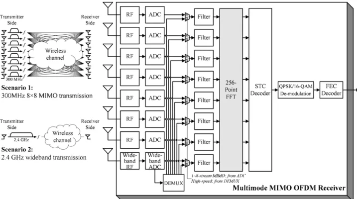
II. SYSTEMSPECIFICATION ANDDESIGNCONSIDERATION To demonstrate the idea of the proposed DVFS FFT pro-cessor, a high-throughput OFDM system supporting up to 300-MHz 8 8 MIMO or 2.4-GHz wideband transmissions with QPSK/16-QAM modulation is considered as our design target. The block diagram of the multimode receiver for this OFDM system is shown in Fig. 1. It consists of eight radio frequency (RF) modules, eight analog-to-digital converters (ADCs), eight filters, a 256-point MIMO FFT processor, a space-time code (STC) decoder, a QPSK/16-QAM demodu-lator, and a forward error correction (FEC) decoder. Based on the two scenarios in Fig. 1, the receiver demodulates 1–8-stream MIMO OFDM signals from multiple antennas or 0018-9200/$25.00 © 2008 IEEE
Fig. 1. Block diagram of the multimode MIMO OFDM receiver.
TABLE I
SPECIFICATION OF THEMULTIMODEMIMO OFDM SYSTEM
a wideband OFDM signal from a single antenna. Thus, the system has high scalability to choose suitable MIMO configu-ration and bandwidth depending on different applications and channel conditions which is the trend for advanced wireless communications. The specification of this MIMO OFDM system is summarized in Table I. It can cover 213.33 ns and 26.67 ns delay spread in MIMO mode and high-speed mode, respectively.
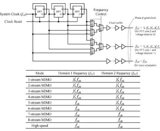
Before designing the DVFS FFT processor for our MIMO OFDM system, two issues should be taken into account. First, to fulfill the system specification in different modes, the 256-point FFT unit needs to support 1–8-stream 300-Msample/s or 2.4-Gsample/s FFT computations. Besides, since the operation mode may be changed from packet to packet, both DFS and DVS schemes must have fast response time to increase the scaling efficiency for low power consumption. To satisfy these two requirements, a novel multimode DVFS FFT processor with fast voltage/frequency scaling is proposed as shown in Fig. 2. It consists of a clock generator, a DVFS controller, a DVS detection unit, and an FFT processing engine. Here we employ a divider-based clock generator to provide different clock frequencies for DFS as shown in Fig. 3. It can achieve fast control of clock phase/frequency compared to the phase-locked loop (PLL). Cooperating with this divided clock, the FFT processing engine in Fig. 2 is designed to support multimode
FFT computations with DVFS capability. FFT inputs are first scheduled by the input scheduler and then calculated by the two FFT cores in different power and clock domains. The minimal supply voltages are estimated by the DVS detection unit where two voltage detectors are employed for each FFT core. Based on these detection results, the off-chip DC-DC converter adjusts its two power supplies to reduce the power consumption. More detailed descriptions of the FFT processing engine and the voltage scaling scheme will be presented in Sections III–VII.
III. RADIX-2 FFT ALGORITHM
Given a complex input sequence , an -point discrete Fourier transform (DFT) is defined as
(1) where is known as the twiddle factor. Due to the high computational complexity in (1), the radix-FFT algorithms which have lower complexity
have been widely adopted in DFT implementations. Besides, since high-radix FFT algorithm has less number of complex multiplications, it is preferred in the hardware design to reduce the number of complex multipliers. As the 256-point FFT comparison shown in Table II, the number of complex mul-tiplication for radix-16 algorithm is 225, which is only about
Fig. 2. Block diagram of the proposed DVFS FFT processor.
Fig. 3. Divider-based clock generator for DFS.
TABLE II
29.3% of that for radix-2 algorithm. Therefore, we choose radix-16 algorithm in our 256-point FFT design. The derivation is described below. Since in (1), we first let
where
where (2)
By (2), (1) can be rewritten as
(3) Eq. (3) can be considered as processing a two-dimensional DFT where each dimension is built by a 16-point DFT. To implement the 16-pint DFT more efficiently, we use the radix-2 FFT algo-rithm which can easily be derived from the radix-2 algoalgo-rithm [8]. By further decomposing the radix-16 DFT into four steps by applying radix-2 index map, we first rewrite and as
where where
(4) By means of (4), the first 16-point DFT in (3) is rewritten as (5), shown at the bottom of the page, where the radix-16 DFT
is completed by the four-step radix-2 algorithm. Similarly, by reformulating and with
where where
(6) The second 16-point DFT in (3) can also be transformed to radix-2 FFT as (7), shown at the bottom of the next page.
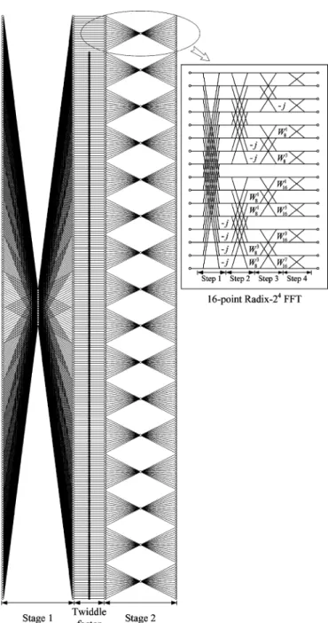
Thus, by (3), (5), and (7), the 256-point radix-2 FFT is fully computed. The corresponding signal flow graph (SFG) of this 256-point FFT is shown in Fig. 4. Note that the 256-point FFT is divided into two stages, where radix-16 FFT algorithm is em-ployed in each stage. The black point between these two stages means that the twiddle factor will be multiplied at that point. Each butterfly of the radix-16 algorithm is further decomposed into four steps. The twiddle factors, and in the second step and in the third step, can be implemented by constant complex multiplications with simple shifters and adders. The canonical signed digit (CSD) technique [9] can also be applied to further reduce the hardware complexity.
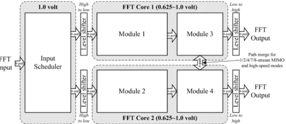
IV. ARCHITECTURE OF THEFFT PROCESSINGENGINE According to the radix-2 algorithm described in Section III, we propose a novel MMDF structure for the FFT processing engine in Fig. 2 supporting DVFS operations and multi-stream computations. This 256-point FFT processing engine consists of an input scheduler, FFT core 1, FFT core 2, and level shifters as shown in Fig. 5. The features of the proposed FFT structure are as follows.
• high throughput rate up to 8-stream 300-Msample/s or 2.4-Gsample/s computations can be provided by using par-allel-8 data-paths;
• multimode operations such as 1–8-stream 256-point FFTs or a high-speed 256-point FFT are supported for MIMO OFDM applications;
Fig. 4. Signal flow graph (SFG) of the radix-2 256-point FFT.
• data-paths are slowed down by the input scheduler in low-throughput modes to support both frequency and voltage scaling;
• radix-2 algorithm and scheduling technique are employed to reduce the number of complex multipliers and the power consumption.
In the proposed MMDF structure, the function of the input scheduler is to rearrange the input order and data rate for FFT core 1 and core 2. Because the operation speed remains the same for all modes, the input scheduler is located in the fixed supply domain (default 1.0 V). After the scheduling, the mul-timode 256-point FFT computations are processed by the two FFT cores in which eight parallel-paths are adopted to increase the maximum throughput. Due to various MIMO configura-tions, FFT core 1 and core 2 are operated in separated power domains (0.625–1.0 V) for independent voltage and frequency scaling as shown in Fig. 5. The FFT cores are further parti-tioned into Module 1 to 4 for detailed explanation. Modules 1 and 2 are used to implement the first radix-2 stage, the twiddle factor multiplications and the first step of the second radix-2 stage. Then, the last three steps of the second radix-2 stage are mapped to Modules 3 and 4. Between the power domain boundaries, high-to-low or low-to-high level shifters are em-ployed for voltage level conversion. More detailed descriptions of each functional block will be given below.
A. Input Scheduler
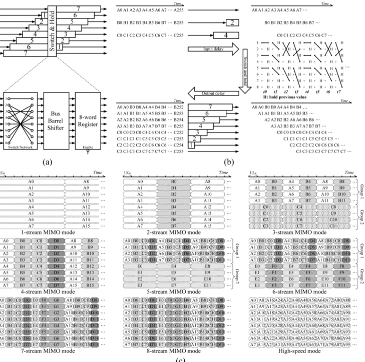
The input scheduler is designed in the FFT processing en-gine for two purposes. One is to schedule the order of the input sequence such that multimode FFT computations can be pro-cessed efficiently and correctly. The other is to distribute the multiple FFT streams into eight paths to slow down the data sample rate in low-throughput modes. Block diagram of the input scheduler is shown in Fig. 6(a). It is composed of seven input delay units, a switch and hold unit, and seven output delay units. The switch and hold unit further consists of a switch network, a bus Barrel shifter [10], and 8-word registers. Here the scheduling of 3-stream MIMO is shown as an example in Fig. 6(b). , , and are the three input streams where is the index number from 0 to 255. These inputs are first adjusted by different input delay and then passed to the switch and hold unit. The initial switch path (at ) is determined by the switch
Fig. 5. Block diagram of the FFT processing engine.
network and the succeeding switching (from to ) is the cyclic shifting of the initial configuration which is performed by the bus Barrel shifter. Since only three streams are distributed into eight data-paths, five-path data are held by registers in each time slot as shown in Fig. 6(b). Afterward, the outputs of the switch and hold unit are adjusted by the output delay units which completes the input scheduling. As we can see, streams A and B with the same index number are scheduled in neighbor that allows the same twiddle factor to be multiplied successively for reduced switching power. Besides, the output sample rate be-comes half and one fourth of the original one such that the FFT cores can work in lower clock frequency. The outputs of the input scheduler for all operation modes are depicted in Fig. 6(c). We can see that every stream inputs are evenly distributed to the eight paths in 1/2/4/7/8-stream MIMO and high-speed modes. As for 3/5/6-stream MIMO mode, the stream inputs are sepa-rated into two groups which has four paths. By this way, the two-group data can be processed using independent clock fre-quencies for better scaling efficiency. Also shown in Fig. 6(c), since the required order for high-speed mode can be obtained from the de-multiplexer (DEMUX) output directly (Fig. 1), the operation of the input scheduling is skipped in this mode.
B. Module 1 and Module 2
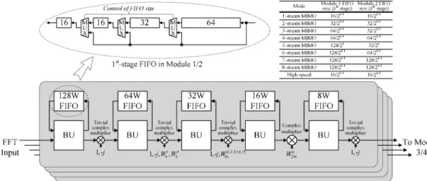
The block diagram of Module 1 (Module 2) with four data-paths is shown in Fig. 7. It consists of five butterfly units (BU), five FIFOs, four trivial complex multipliers, and a complex mul-tiplier in each path. Module 1 and 2 are mapped from the four-step radix-2 algorithm to implement the first radix-2 stage, the twiddle factor multiplications and the first step of the second radix-2 stage in Fig. 4. Since the parallel 8-path FFT structure does not have a path merging (data for BU processing come from different paths) until the final three steps, each path in Module 1 and 2 has independent data flow as shown in Fig. 7. Besides, to support MIMO FFT, the FIFO size is configured ac-cording to the stream number such that data with correct indexes can be acquired by BU to perform complex addition and sub-traction. Take the first-stage FIFO for example, the FFT inputs and must arrive at BU inputs simultaneously to implement the radix-2 algorithm. In 1/2/4/7/8-stream MIMO and high-speed modes, the FFT inputs are evenly distributed into eight paths as shown in Fig. 6(c). Therefore, the FIFO size should be -word where is the total stream number. As for
3/5/6-stream MIMO mode, since Modules 1 and 2 work sep-arately (inputs are distributed into four paths), the FIFO size should be -word where is the stream number processed by the corresponding Module. Thus, the structure of the first-stage FIFO can be found in Fig. 7 where a table of FIFO size is also included. Among the BU outputs, only the fourth stage adopts complex multipliers for twiddle factor multiplication. The trivial twiddle factors in other stages can be implemented with simple constant multipliers and multiplexers (MUXs).
C. Module 3 and Module 4
The block diagram of Module 3 and 4 is depicted in Fig. 8. They consist of 16 BUs, eight FIFOs, eight trivial complex multipliers, and eight MUXs. Module 3 and 4 are responsible to calculate the last three steps of the second radix-2 stage in Fig. 4. For 3/5/6-stream MIMO modes, since these two Modules work independently, the MUXs are configured such that there is no data transfer between Modules 3 and 4. On the other hand, only the four first-stage BUs in Module 4 are required (first-stage BUs in Module 3 are skipped) to perform the path merging for 1/2/4/7/8-stream MIMO and high-speed modes. Similar to Modules 1 and 2, the FIFO size also depends upon the stream number as shown in Fig. 8. Note that for 1/2/4/7/8-stream MIMO and high-speed modes, no FIFO is required because the data can be directly acquired by BU from different paths.
V. OPEN-LOOPVOLTAGEDETECTION ANDSCALINGSCHEME For DVFS designs, a robust, accurate, and fast voltage scaling mechanism is important to insure the chip performance and to reduce the power consumption. However, due to the increasing chip variation in advanced process technologies, it is difficult to achieve these three goals simultaneously. Traditionally, the voltage scaling scheme can be categorized into two types. One is to scale the supply voltage to a predetermined value from sim-ulated results for each operation frequency [3], [4], and the other is to perform real-time voltage detection and scaling during the chip operations [5]–[7]. For the first method, because of the process uncertainty, the scaled supply voltage is estimated from worst-case simulation. Although the correct chip functionality can be assured in these designs; however, the scaling efficiency for power consumption is low due to a conservative voltage re-duction. To reach more optimal scaling results, the real-time
Fig. 6. (a) Block diagram. (b) 3-stream MIMO operation. (c) Output of the input scheduler. voltage detection has been proposed using a critical-path replica
to monitor the functionality under different supply voltages [5]–[7]. In these detection-based designs, different control algorithms have been proposed for aggressive voltage scaling and robust operations, but long convergence time is required for the scaling operation. This is because that the voltage must be decreased gradually to find the optimal operation point without causing any errors. For our DVFS FFT processor, since the operation mode may switch rapidly from packet to packet, a fast voltage detection scheme is demanded to increase the scaling efficiency.
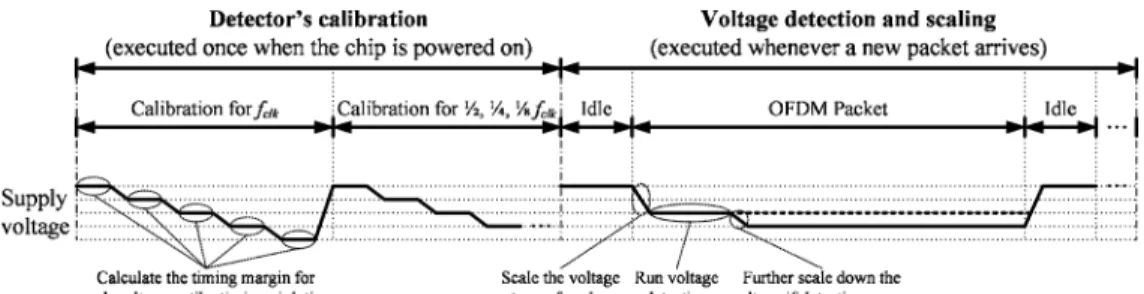
To achieve better scaling efficiency, we propose an open-loop voltage detection and scaling mechanism with calibration. At the beginning, the detector’s calibration is performed once when the chip is powered on as shown in Fig. 9. For each
op-eration frequency (1, 1/2, 1/4, and 1/8 ), the timing margin is calculated from high to low voltages until a timing violation occurs. After all the timing information is collected in the detector’s calibration, the proposed OLVDS scheme switches to the voltage detection and scaling mode for FFT processing. Whenever a new OFDM packet arrives (in different operation modes), the supply voltage is scaled to a “safe” voltage shortly according to the calibration data for the current operation frequency. Thus, fast and robust voltage scaling can be easily achieved. Besides, voltage detection for further voltage scaling is then performed during FFT processing to take account of voltage and temperature variations. By calculating the timing margin for the target voltage without changing the supply voltage, the proposed detection method decides if further voltage reduction can be applied with fast response. The
de-Fig. 7. Block diagram of Module 1/2 in the FFT processing engine.
Fig. 8. Block diagram of Module 3 and 4 in the FFT processing engine.
tailed OLVDS design and its operation procedure are described as follows.
A. Hardware Structure of the OLVDS Design
Block diagram of the proposed OLVDS design is shown in Fig. 10. It consists of a DVFS controller, two voltage detec-tors, an off-chip DC-DC converter, a clock generator, and level shifters for voltage level conversion. Each voltage detector in-cluding four identical detection units is responsible to detect the minimal supply voltage for one FFT core. To take geom-etry variation into account, the detection units are placed in different chip locations. Each detection unit further comprises
of two D-type flip-flops (DFF) as I/O registers, a critical-path replica of the FFT core, and a tunable delay line. As shown in Fig. 10, the critical-path replica is built by a series of delay line cells and inverters with balance rise/fall time. These delay line cells have the same channel length as other logic cells such that they have similar delay characteristics over different voltages. Here the inverters are employed to balance the overall rise/fall delay of the critical-path replica. In our current design, addi-tional 160 picosecond delay (in nominal voltage) is included in the critical-path replica as the design margin accounting for PVT variations and the mismatch of critical-path replica. The tunable delay line is built by buffer (BUF) and transmission-gate MUX
Fig. 9. Scheduling of the proposed OLVDS scheme.
Fig. 10. Block diagram of the proposed OLVDS design.
cells with balanced rise/fall time. The overall OLVDS design is verified at design time by running fast SPICE simulation under corner conditions.
B. Operations of the OLVDS Scheme
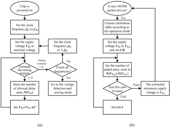
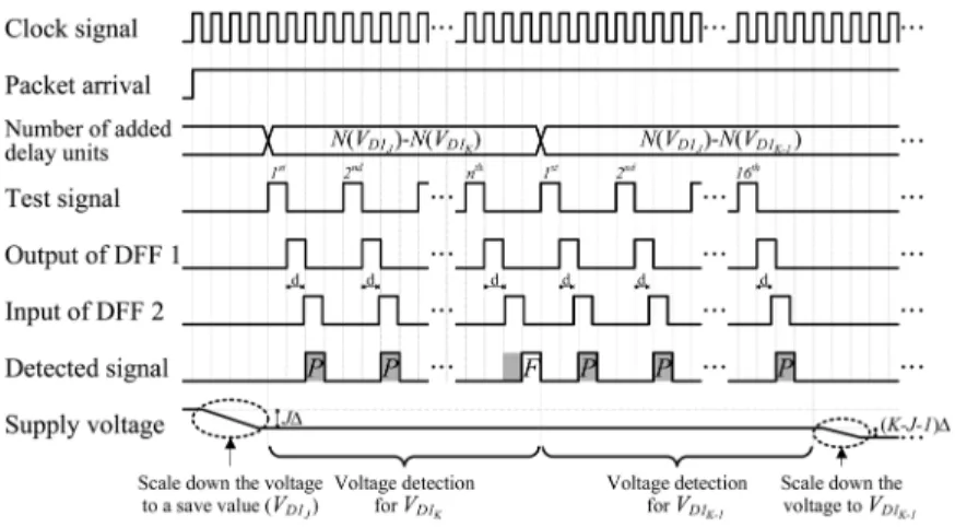
Since the same OLVDS operation is employed for the two power domains, only the control flow for domain 1 is depicted in Fig. 11 for simplicity. When the chip is powered on as shown in Fig. 11(a), OLVDS starts in the detector’s calibration mode. At the beginning, the operation frequency is set to and supply voltage is set to the nominal value (1.0 volt) for timing margin estimation. Here we define one BUF plus one MUX in Fig. 10 as the delay unit. As the timing chart shown in Fig. 12, a one-cycle pulse train is used as the test signal for the voltage detector in Fig. 10. If the delay under test (critical-path replica plus tunable delay line) is longer than the clock period, the detected signal will be shifted from its expected position. To estimate the timing margin in , the number of added delay units in the tunable delay line is swept from 59 to 0 to find the number of allowed
delay units (timing margin) which is to be saved in the table. If this number is greater than or equal to 0, the supply voltage is scaled down by (25 mV) and the same timing margin esti-mation is performed. This procedure repeats until the delay of critical-path replica is longer than the clock period (timing vi-olation) in a certain voltage as shown in Fig. 12. In this way, a calibration table for can be obtained as shown in Table III where is the number of allowed delay units in . Because four clock frequencies (1, 1/2, 1/4, and 1/8 ) are adopted for different operation modes in the proposed design, the calibration tables for 1/2, 1/4, and 1/8 must also be gen-erated as shown in Fig. 11(a) for further voltage detection and scaling operations.
After the calibration tables for all operation frequencies are collected in the detector’s calibration mode, OLVDS goes to the voltage detection and scaling mode. As shown in Fig. 11(b), whenever a new OFDM packet arrives, the corresponding calibration table is chosen according to the operation mode of the incoming packet. Here we assume that the minimal supply
Fig. 11. Control flow of the OLVDS scheme for domain 1. (a) Detector’s calibration mode. (b) Voltage detection and scaling mode.
Fig. 12. Timing chart in the detector’s calibration for domain 1.
TABLE III CALIBRATIONDOMAIN1
voltage is from the calibration table and the “safe” voltage is which is higher than . The supply voltage is scaled to for low power at the beginning of the packet. Then the critical-path replica plus additional
delay units (from tunable delay line) are tested for 16 times to see if the voltage can be scaled to
. If all 16 tests pass, the supply voltage is scaled to to save more power. Otherwise, a higher voltage is tested again and the procedure repeats. An example is given in Fig. 13 for illustration. In this example, the th test signal for is not received in the correct cycle which means is not a stable voltage for chip operations. Therefore, the number
of added delay units is set to for
detection of . Since all 16 tests for are passed in this example, further can be reduced in the supply voltage. As described above, the proposed OLVDS scheme does not adjust the supply voltage for voltage detection, and therefore it has fast response time. Besides, the voltage detection has good accuracy by taking account of real-time
Fig. 13. Timing chart in the voltage detection and scaling for domain 1.
Fig. 14. Chip micrograph.
voltage and temperature variations during packet receiving (FFT processing).
VI. CHIPIMPLEMENTATION
At the beginning of the chip design, the parallelized radix-2 FFT algorithm is coded in MATLAB language. From fixed-point simulation, 8-bit input wordlength and 11-bit output wordlength are chosen and the implementation loss is within 0.1 dB for QPSK/16-QAM modulation at 17 dB signal-to-noise ratio (SNR). The resulting signal-to-quantization-noise ratio (SQNR) of this 256-point FFT processor is over 35.8 dB. Then the architecture of the proposed FFT processor is modeled in Verilog and functionally verified using NC-Verilog simulator. Besides, we also use UltraSim mixed-mode simulator with Verilog/SPICE language to verify the DVFS operation under different process and temperature conditions. A test chip of the proposed DVFS FFT processor has been fabricated in UMC 90-nm single-poly nine-metal (1P9M) CMOS process. The core size including the test module is 1.88 1.88 mm as shown in Fig. 14. The gate count of the OLVDS design (including DVFS controller and voltage detectors) is only 4.6 K which occupies 0.8% of the chip gate count. Due to the speed limitation of chip I/O, a digitally controlled oscillator (DCO) [11] and 11.3-kbit two-port SRAM with 8 banks are employed in the test module for high-speed testing. FFT inputs are first read from the input pins and stored to SRAM serially using the external clock (normal-speed). Then, the DVFS FFT processor
TABLE IV
CHIPSUMMARY OF THEPROPOSEDDVFS FFT PROCESSOR
starts to calculate 256-point FFT in parallel from the eight-bank outputs of SRAM using the DCO clock (high-speed). After the results are stored back to SRAM, it can be read from the output pins serially using the external clock. This chip is packaged in a 144-pin CQFP where 85 pins are signal pins and others are power pins.
VII. MEASUREMENTRESULT ANDANALYSIS
In order to verify the proposed ideas, fifteen chips from three process corners (TT, SS, and FF) have been packaged for testing. These chips are measured using Agilent 93000 SOC test system and the chip summary is shown in Table IV. The maximum throughput of our proposed FFT IC in TT corner is up to 3.58 Gsample/s at the nominal voltage. The power consumption for 8-stream 300-Msample/s FFTs and a 2.4-Gsample/s FFT is 160.5 mW and 145.5 mW, respectively (TT corner at 1.0 V). Besides, the voltage detection result and the scaled power performance for all operation modes are also measured. As shown in Table V, the differences between the detected and the required supply voltages are within 0.1 V for all process corners without causing functional errors (in steps of 25-mV resolution). This voltage detection error mainly comes from the critical-path replica and it can be improved by adopting more sophisticated designs [5], [12]. The power
Fig. 15. Measured power consumption under different operation modes (TT corner).
TABLE V
DETECTEDSUPPLYVOLTAGE ANDREQUIREDSUPPLYVOLTAGE
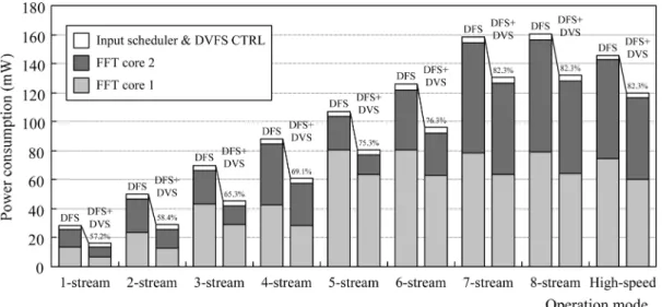
consumption of the proposed FFT processor with voltage/fre-quency scaling is shown in Fig. 15. As we can see, the chip power scales with the throughput rate when DFS is employed. Therefore, the overall power consumption can be optimized for the MIMO OFDM system. Moreover, additional 18% to 43% of the total power can be saved by further including the DVS scheme.
For comparison, the traditional method adopting eight single-path delay feedback (SDF) structures [8] is also implemented with clock gating and the same radix-2 algorithm is adopted in this reference design. Assuming all operation modes have equal operation period, the averaged power consumption for different process corners is shown in Fig. 16. When only DFS is activated in our DVFS FFT chip, about 10% of power consumption can be saved which results mainly from the scheduling of multipli-cation as described earlier. In DFS mode, it is also found that
the proposed chip in FF corner has the maximum power con-sumption among process corners due to large leakage power. This effect can be compensated after DVS is turned on since the chip in FF corner has more timing margin for voltage scaling. The averaged power reduction by DVS is from 11% to 33% for the three process corners and the overall power saving including both DFS and DVS is 39%, 31%, and 19% for FF, TT, and SS corners, respectively. Finally, the chip comparison is given in Table VI. Here we choose two variable-length FFT chips sup-porting 256-point FFT [13], [14] to compare the energy effi-ciency. Besides, to mitigate the impact of different technologies and wordlength, the normalized FFTs per energy shown in (8) [15] is employed as the performance index. From Table VI, we can find that [14] and our proposed FFT processor have similar energy efficiency which is higher than that of [13]. However, it should be noted that the FFT processor in [14] is a full-custom
Fig. 16. Averaged power consumption for different process corners.
TABLE VI FFT CHIPCOMPARISON
design working in the subthreshold region (350 mV) for very low-throughput applications. See equation (8) at the bottom of the previous page.
VIII. CONCLUSION
In this paper, a novel DVFS FFT processor for high-throughput and low-power MIMO OFDM systems has been proposed. By the proposed MMDF architecture and OLVDS scheme, our FFT processor can process 1–8-stream 300-Msample/s 256-point FFTs or a 2.4-Gsample/s 256-point FFT at minimum voltage/frequency. Besides, a parallelized radix-2 FFT structure is adopted to save the power consump-tion and hardware cost of complex multipliers. A test chip of the proposed FFT processor has been designed and fabricated using UMC 90-nm single-poly nine-metal CMOS process with a core area of 1.88 1.88 mm . The SQNR performance of this FFT processor is over 35.8 dB to support QPSK/16-QAM modulation. Power dissipation of 2.4 Gsample/s 256-point
FFT computations is about 119.7 mW at 0.85 V. Compared to the traditional method, the averaged power reduction by the proposed DVFS FFT design is 39%, 31%, and 19% for FF, TT, and SS corners, respectively.
ACKNOWLEDGMENT
The authors would like to thank their colleagues of the SI2 group of National Chiao Tung University for many fruitful dis-cussions, and National Chip Implementation Center (CIC) for providing chip testing services. The shuttle program supported by UMC is acknowledged as well.
REFERENCES
[1] Y.-W. Lin and C.-Y. Lee, “Design of an FFT/IFFT processor for MIMO OFDM systems,” IEEE Trans. Circuits Syst. I, Reg. Papers, vol. 54, no. 4, pp. 807–815, Apr. 2007.
[2] Y. Chen, Y.-W. Lin, and C.-Y. Lee, “A block scaling FFT/IFFT pro-cessor for Wimax applications,” in Proc. 2nd IEEE Asian Solid-State
[3] K. J. Nowka, G. D. Carpenter, E. W. MacDonald, H. C. Ngo, B. C. Brock, K. I. Ishii, T. Y. Nguyen, and J. L. Burns, “A 32-bit powerPC system-on-a-chip with support for dynamic voltage scaling and dy-namic frequency scaling,” IEEE J. Solid-State Circuits, vol. 37, no. 11, pp. 1441–1447, Nov. 2002.
[4] T. Fujiyoshi, S. Shiratake, S. Nomura, T. Nishikawa, Y. Kitasho, H. Arakida, Y. Okuda, Y. Tsuboi, M. Hamada, H. Hara, T. Fujita, F. Ha-tori, T. Shimazawa, K. Yahagi, H. Takeda, M. Murakata, F. Minami, N. Kawabe, T. Kitahara, K. Seta, M. Takahashi, Y. Oowaki, and T. Furuyama, “A 63-mW H.264/MPEG-4 audio/visual codec LSI with module-wise dynamic voltage/frequency scaling,” IEEE J. Solid-State
Circuits, vol. 41, no. 1, pp. 54–62, Jan. 2006.
[5] M. Nakai, S. Akui, K. Seno, T. Meguro, T. Seki, T. Kondo, A. Hashiguchi, H. Kawahara, K. Kumano, and M. Shimura, “Dynamic voltage and frequency management for a low-power embedded mi-croprocessor,” IEEE J. Solid-State Circuits, vol. 40, no. 1, pp. 28–35, Jan. 2005.
[6] T. Kuroda, K. Suzuki, S. Mita, T. Fujita, F. Yamane, F. Sano, A. Chiba, Y. Watanabe, K. Matsuda, T. Maeda, T. Sakurai, and T. Fu-ruyama, “Variable supply-voltage scheme for low-power high-speed CMOS digital design,” IEEE J. Solid-State Circuits, vol. 33, no. 3, pp. 454–462, Mar. 1998.
[7] M. Nomura, Y. Ikenaga, K. Takeda, Y. Nakazawa, Y. Aimoto, and Y. Hagihara, “Delay and power monitoring schemes for minimizing power consumption by means of supply and threshold voltage control in active and standby modes,” IEEE J. Solid-State Circuits, vol. 41, no. 4, pp. 805–814, Apr. 2006.
[8] S. He and M. Torkelson, “Designing pipeline FFT processor for OFDM (de)modulation,” in 1998 URSI Int. Symp. Signal, Systems, Electronics.
Conf. Proc., Pisa, Italy, Oct. 1998, vol. 29, pp. 257–262.
[9] K. K. Parhi, VLSI Digital Signal Procesing Systems: Design and
Im-plementation. New York: Wiley, 1999.
[10] L. G. Johnson, “Conflict free memory addressing for dedicated FFT hardware,” IEEE Trans. Circuits Syst. II, vol. 39, no. 5, pp. 312–316, May. 1992.
[11] B. Giebel, J. Lutz, and P. L. O’Leary, “Digitally controlled oscillator,”
IEEE J. Solid-State Circuits, vol. 24, no. 3, pp. 640–645, Jun. 1989.
[12] A. Drake, R. Senger, H. Deogun, G. Carpenter, S. Ghiasi, T. Nguyen, N. James, M. Floyd, and V. Pokala, “A distributed critical-path timing monitor for a 65 nm high-performance microprocessor,” in IEEE Int.
Solid-State Circuits Conf. (ISSCC) Dig. Tech. Papers, Feb. 2007, pp.
398–399.
[13] G. Zhong, F. Xu, and A. N. Willson, “A power-scalable reconfigurable FFT/IFFT IC based on a multi-processor ring,” IEEE J. Solid-State
Cir-cuits, vol. 41, no. 2, pp. 483–495, Feb. 2006.
[14] A. Wang and A. Chandrakasan, “A 180-mV subthreshold FFT pro-cessor using a minimum energy design methodology,” IEEE J.
Solid-State Circuits, vol. 40, no. 1, pp. 310–319, Jan. 2005.
[15] B. M. Bass, “A low-power, high-performance, 1024-point FFT pro-cessor,” IEEE J. Solid-State Circuits, vol. 34, no. 3, pp. 380–387, Mar. 1999.
Yuan Chen (S’06) was born in Taipei, Taiwan,
R.O.C., in 1976. He received the B.S. degree in electrical engineering from National Tsing Hua Uni-versity, Hsinchu, Taiwan, R.O.C., in 1998, and the M.S. degree in communications engineering from National Chiao Tung University, Hsinchu, Taiwan, R.O.C., in 2000. He is currently working toward the Ph.D. degree with the Department of Electronics Engineering, National Chiao Tung University.
From 2000 to 2004, he was with ITRI/CCL working in the area of cable modem/TV and optical networking. His research interests include communication signal processing, VLSI architectures, and low-power high-throughput chip designs.
Yu-Wei Lin was born in Tainan, Taiwan, R.O.C.,
in 1975. He received the B.S. degree in electrical engineering from National Sun Yat-Sen University, Kaohsiung, Taiwan, R.O.C., in 1999 and the M.S. and Ph.D. degrees from National Chiao Tung Uni-versity, Hsinchu, Taiwan, R.O.C., in 2003 and 2005, respectively.
In 2005, he joined MediaTek Inc., Hsinchu, Taiwan, to develop digital TV and mobile TV modem related systems. His research interests include baseband signal processing, VLSI architec-tures, and SoC designs for communication systems.
Yu-Chi Tsao was born in Taipei, Taiwan, R.O.C.,
in 1983. He received the B.S. degree in electrical engineering from National Chung Cheng University, Min-Hsiung Chia-Yi, Taiwan, R.O.C., in 2005, and the M.S. degree in electronics engineering from National Chiao Tung University, Hsinchu, Taiwan, R.O.C., in 2007.
His research interests include VLSI architectures and SoC designs for communication systems.
Chen-Yi Lee (M’01) received the B.S. degree from
National Chiao Tung University, Hsinchu, Taiwan, R.O.C., in 1982, and the M.S. and Ph.D. degrees from Katholieke University Leuven, Belgium, in 1986 and 1990, respectively, all in electrical engineering.
From 1986 to 1990, he was with IMEC/VSDM, working in the area of architecture synthesis for DSP. In February 1991, he joined the faculty of the Electronics Engineering Department, National Chiao Tung University, Hsinchu, Taiwan, R.O.C., where he is currently a Professor and Department Chair. His research interests mainly include VLSI algorithms and architectures for high-throughput DSP applications. He is also active in various aspects of high-speed networking, system-on-chip design technology, very low power designs, and multimedia signal processing. He served as the Director of Chip Implementation Center (CIC), an organization for IC design promotion in Taiwan.
Dr. Lee was the former IEEE CAS Taipei Chapter Chair (2000–2001) and the microelectronics program coordinator (2003–2005) of Engineering Division under the National Science Council of Taiwan.