Dielectric characteristics of nanocrystalline Ag – Ba 0.5 Sr 0.5 Ti O 3 composite thin
films
K. P. Jayadevan, C. Y. Liu, and T. Y. Tseng
Citation: Applied Physics Letters 85, 1211 (2004); doi: 10.1063/1.1780596
View online: http://dx.doi.org/10.1063/1.1780596
View Table of Contents: http://scitation.aip.org/content/aip/journal/apl/85/7?ver=pdfcov
Published by the AIP Publishing
Articles you may be interested in
Double dielectric relaxations in SnO 2 nanoparticles dispersed in conducting polymer
J. Appl. Phys. 102, 084110 (2007); 10.1063/1.2798982
Structure, dielectric, and piezoelectric properties of CuO-doped K 0.5 Na 0.5 Nb O 3 – Ba Ti O 3 lead-free ceramics
J. Appl. Phys. 102, 074113 (2007); 10.1063/1.2787164
Two distinct dielectric relaxation mechanisms in the low-frequency range in Bi 5 Ti Nb W O 15 ceramics
Appl. Phys. Lett. 88, 162908 (2006); 10.1063/1.2191953
Dielectric properties of Si – Ba 0.5 Sr 0.5 Ti O 3 composite thin films elaborated by pulsed laser deposition
J. Appl. Phys. 98, 034106 (2005); 10.1063/1.1999852
Ferroelectric domain wall relaxation in Ba 0.25 Sr 0.75 Ti O 3 films displaying Curie-Weiss behavior
J. Appl. Phys. 96, 4392 (2004); 10.1063/1.1787587
This article is copyrighted as indicated in the article. Reuse of AIP content is subject to the terms at: http://scitation.aip.org/termsconditions. Downloaded to IP: 140.113.38.11 On: Thu, 01 May 2014 04:14:45
Dielectric characteristics of nanocrystalline Ag– Ba
0.5Sr
0.5TiO
3composite thin films
K. P. Jayadevan, C. Y. Liu, and T. Y. Tsenga)
Department of Electronics Engineering and Institute of Electronics, National Chiao-Tung University, Hsinchu 300, Taiwan, Republic of China
(Received 31 October 2003; accepted 10 June 2004)
Nanocrystalline Ag– Ba0.5Sr0.5TiO3(Ag–BST) composite thin films are deposited on Pt/Ti/SiO2/ Si
substrates by a sol-gel method. The voltage-dependent capacitance共C–V兲 and dielectric loss of the films decrease with increasing Ag up to 2 mol % due to a series configuration involving low dielectric interface layers and dense microstructures. The evidence for asymmetric distribution of charge carriers in the Ag–BST film is derived from C – V measurements. The dielectric tunability of BST film with 1 mol % Ag is comparable to that of pure BST. © 2004 American Institute of Physics. [DOI: 10.1063/1.1780596]
There had been interest in the past several decades to discover the versatile nature of silver(Ag) in modifying the microstructure and resultant physical properties such as di-electric characteristics of insulators1,2 and superconductivity of cuprates,3 and recently, optical nonlinearity of Ag-dielectric composites.4 Despite the sustained focus on the Ag-dielectric composites, there is lack of adequate consis-tency on how Ag affects the resultant dielectric properties of bulk Ag– BaTiO3 (BTO) (Refs. 5–7) and thin films of Ag–
BTO (Ref. 8) and Ag–共Ba,Sr兲TiO3 (BST).9 The sol-gel-derived Ag–BTO nanocomposite thin films8 showed a de-crease in dielectric constant due to a reduction in net polarization of Ag–BTO and an increase in loss with increas-ing Ag up to 5 mol %. In contrast, the pulsed-laser-deposited (PLD) Ag-BST thin films9
exhibited higher capacitance for 5 wt. % Ag-doped samples, which was ascribed to the im-proved oxygenation of the BST film, as metastable silver oxide phases decomposed during the thermal processing of the film and filled the oxygen vacancies. However, no dielec-tric loss characteristics were discussed.9 In this letter, we report the effect of Ag addition on the capacitance and loss characteristics of sol-gel-derived Ba0.5Sr0.5TiO3 thin films. Ba0.5Sr0.5TiO3, which is a high permittivity, low loss
paraelectric material suitable for integrated capacitor applications,10 in combination with small amounts of Ag would form a potential metal-dielectric composite for elec-tromagnetic wave propagation.
The pure Ba0.5Sr0.5TiO3 (BST) and (1 mol % and 2 mol %) Ag–(99 mol % and 98 mol %) Ba0.5Sr0.5TiO3
(Ag(1)–BST and Ag(2)–BST) thin films were prepared by an acetate precursor sol-gel route.11Stoichiometric amounts of the starting materials, Ba共OAc兲2, Sr共OAc兲2, Ag(OAc), and
Ti共i-OPr兲4 (OAc-Acetate, i-OPr-Isopropoxide), were
dis-solved in acetic acid and ethylene glycol (3:1) and stirred at 90 ° C for about 60 min. The above prepared 0.15 M precursor solutions were spin-coated on Pt共100 nm兲/Ti共5 nm兲/SiO2共500 nm兲/Si substrates in two steps(1000 rpm for 15 s and 4000 rpm for 60 s) in order to achieve a uniform coating. Each deposited layer was heat-treated at 200 ° C for 10 min and then 500 ° C for 30 min. The coating and pyrolysis steps were repeated to obtain the desired film thickness. The films were finally annealed at
700 ° C for 2 h in air and characterized for phase formation and grain size using x-ray diffraction (XRD, Cu K␣, = 0.15405 nm, 0.02° 2 step, Rigaku DMaxB x-ray diffrac-tometer), and microstructure using scanning electron micros-copy(SEM, Hitachi S4700). For dielectric characterization, metal-insulator-metal (MIM) structures were fabricated by depositing 100 nm thick Pt top electrodes with a diameter of 250m by electron beam evaporation through a shadow mask. The capacitance–voltage 共C–V兲 and dielectric loss characteristics were measured using HP4284A LCR Meter from −6 to + 6 V and back with a step voltage of 0.1 V at 100 kHz.
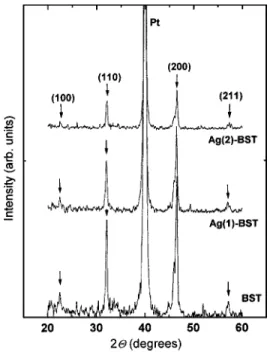
Figure 1 shows the XRD patterns of BST, Ag(1)–BST, and Ag(2)–BST films. All the diffraction peaks are indexed to BST phase with(200) being the most intense peak in all the three samples. As silver oxides are unstable12 at the an-nealing temperature 共700 °C兲, the presence of any oxide phases of silver is ruled out in the Ag-BST films. The dif-fraction peaks of Ag(1)–BST and Ag(2)–BST do not show any shifts with reference to those of pure BST when recorded for three sets of samples, indicating negligible solubility of
a)Electronic mail: [email protected] FIG. 1. XRD patterns of BST, Ag(1)–BST, and Ag(2)–BST thin films.
APPLIED PHYSICS LETTERS VOLUME 85, NUMBER 7 16 AUGUST 2004
0003-6951/2004/85(7)/1211/3/$20.00 1211 © 2004 American Institute of Physics
This article is copyrighted as indicated in the article. Reuse of AIP content is subject to the terms at: http://scitation.aip.org/termsconditions. Downloaded to IP: 140.113.38.11 On: Thu, 01 May 2014 04:14:45
Ag in BST. The gradual reduction in intensities of diffraction peaks for Ag(1)–BST and Ag(2)–BST could have been caused by an increase in the degree of disorder in the orien-tation of the crystallites induced by the modification of grain boundary atomic configuration by Ag.9The full-width at half maxima(FWHM,) of (110) and (200) peaks and the aver-age grain sizes共tXRD= 21± 2 nm兲 obtained by Scherrer equa-tion at corresponding Bragg angles, B, (tXRD
= 0.9/cosB, where is the wavelength of the Cu K␣ radiation) remain unchanged, as the amounts of Ag added are insufficient to form an enough second phase and affect these parameters.
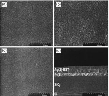
Figure 2 depicts the SEM analysis of the surface mor-phologies of BST, Ag(1)–BST and Ag(2)–BST films and cross section for the Ag(2)–BST film. For pure BST, the SEM study reveals fairly uniform agglomerates with average diameter共dSEM兲 of ⬃27 nm [Fig. 2(a)]. An increase in
non-uniformity is observed for the dSEMof Ag(1)–BST film with
an average value of ⬃40 nm [Fig. 2(b)] that differs much from the primary particle or grain size obtained by XRD tXRD. The presence of nonuniform agglomerates on the sur-face of the Ag(1)–BST film has been found to be reproduc-ible upon the SEM examination of surface morphology of four samples. The formation of large and dense Ag(1)–BST agglomerates could be due to the enhanced grain boundary diffusion caused by the space charge effect across the Ag/ BST interfaces as a result of Fermi energy equalization upon the addition of a small and critical amount of Ag.5–7For the Ag(2)–BST film, the agglomerate size共dSEM⬃25 nm兲 is
highly uniform with no large ones observed. The microstruc-ture is better than pure BST and Ag(1)–BST with consider-able reduction in porosity[Fig. 2(c)], which could be due to the low solubility of Ag in BST grains and its increased presence along the grain boundaries.9 The cross-sectional SEM analysis [not shown here for BST and Ag(1)–BST] indicates that the 210± 10 nm thick films on Pt/ Ti/ SiO2/ Si have clearly distinguishable, crack-free interfaces. The dense microstructure of Ag(2)–BST is further demonstrated by a cross-sectional SEM picture as shown in Fig. 2(d).
The C – V characteristics for pure BST, Ag(1)–BST, and Ag(2)–BST films in the range from −6 to +6 V are pre-sented in Fig. 3. The C – V curve for pure BST under increas-ing and decreasincreas-ing field has identical position for maximum effective capacitance共Cm兲. No broadening of the C–V curve is observed for Ag(1)–BST despite a reduction in capacitance relative to pure BST and a slight positive shift共⬃+0.1 V兲 of the Cmin the down field. For the Ag(2)–BST film, the C–V curve broadens and is associated with lowering and shifting of the Cm to ⬃ +0.2 V in the down field. These observa-tions can be explained as follows: As obtained from the SEM analysis, the BST and Ag–BST have typical microstructures that are reminiscent of films prepared by solution deposition route with randomly oriented nanocrystalline grains aligned parallel to the substrate. Therefore, the effective capacitance 共Ceff兲, which comprises the contributions from the grain
in-terior of the film 共Cgf兲, film/electrode interface 共Ci兲, and grain boundary共Cgb兲, can be expressed in a series capacitor
configuration13as,
1/Ceff= 1/Cgf+ 1/Ci+ 1/Cgb. 共1兲
Of the three terms, the reduction in Ceff of the Ag(1)–BST and Ag(2)–BST films could have been caused by the low Cgb, since Ag has limited solubility in the BST lattice and is
expected to modify the grain boundary atomic configuration.9 In a nanocrystalline sample, Cgb is predomi-nant. The formation of a film/electrode interfacial layer with a low Ci cannot be ruled out as Ag might diffuse to the interface. The consequences of such grain boundary modifi-cation or low dielectric interface formation are a reduction in Ceffand a slight shift in the C – V maxima of Ag(1)–BST and Ag(2)–BST films when measured down field indicative of an asymmetric distribution of the charge carriers in the film. The product Cm⫻⌬V is a measure of the accumulated charge where Cmis the maximum effective capacitance and ⌬V is the corresponding voltage shift.13
That the ⌬V is greater for Ag(2)–BST implies an increase in charge accu-mulation with increasing Ag in BST. The positive C – V
FIG. 2. SEM pictures of surface morphologies of sol-gel-derived(a) BST, (b) Ag(1)–BST, (c) Ag(2)–BST thin films, and (d) cross-sectional SEM pic-ture of Ag(2)–BST film 共thickness⬃210±10 nm兲 on Pt/Ti/SiO2/ Si
sub-strates indicating dense microstructure. FIG. 3. C – V characteristics of BST, Ag(1)–BST, and Ag(2)–BST films mea-sured in the range −6↔ +6 V.
1212 Appl. Phys. Lett., Vol. 85, No. 7, 16 August 2004 Jayadevan, Liu, and Tseng
This article is copyrighted as indicated in the article. Reuse of AIP content is subject to the terms at: http://scitation.aip.org/termsconditions. Downloaded to IP: 140.113.38.11 On: Thu, 01 May 2014 04:14:45
shifts14 for Ag(1)–BST and Ag(2)–BST upon reversing the field indicate the presence of excess negatively charged spe-cies(electrons from Ag) near to the top electrode, which also indirectly points to the direction of diffusion of the Ag as towards the surface of the film, thereby modifying the top electrode/film interface. The identical position of Cmfor pure BST in either sweeps confirms the absence of accumulated charge.
It is interesting to note that the tunability(=C0− CV/ C0,
where C0and CV are the capacitance at zero and maximum bias voltages) of the C–V curve for Ag(1)–BST film 共22±2%兲 is comparable or marginally higher than pure BST共21±2%兲. Improvement in dielectric tunability is often associated with better crystallinity of the film. In this case, on the contrary, we observe a reduction in intensity of the diffraction peaks as shown by XRD, without lowering of tunability. This observation may be correlated to the typical microstructure, which shows that the 1 mol % Ag addition improves the densification of the BST nanograins forming large agglomerates[Fig. 2(b)]. The large agglomerates may have grains with identical polarization behavior causing an increase in polarization density, which results in the observed dielectric tunability being equal or marginally better than pure BST. The significant broadening of the capacitance with a reduction in tunability 共15±2%兲 for Ag(2)–BST film is due to the inability of the dipole moments in the BST nan-ograins to orient in the presence of applied field because of the enhanced pinning effect of Ag(Ref. 9) along the grain boundaries, as the SEM picture [Fig. 2(c)] reveals the ab-sence of large agglomerates of Ag(2)–BST unlike that of the Ag(1)–BST film [Fig. 2(b)]. The average dielectric constants for the Cmof BST, Ag(1)–BST and Ag(2)–BST correspond to 237, 222, and 182, respectively with⬃±10 variation.
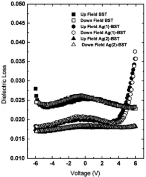
Figure 4 shows the dielectric loss 共tan␦兲 of pure BST, Ag(1)–BST, and Ag(2)–BST films. At zero bias voltage,
tan␦ decreases in the order of BST 共0.025兲⬎Ag共1兲–BST 共0.02兲⬎Ag共2兲–BST (0.018) with ⬃±0.001 variation. For the entire range of measurement (−6↔ +6 V or −286↔ + 286 kV/ cm), the tan␦ of Ag(2)–BST is the lowest. The dense microstructure of Ag(2)–BST is one of the reasons for the lowest loss. As the nonagglomerated nanocrystalline Ag(2)–BST grains have more grain boundaries [Fig. 2(c)], and relaxational loss from the grain boundaries is negligible,15 a reduction in loss characteristics is expected. Moreover, the presence of small amounts of Ag along grain boundaries or interfaces enhances the polarization pinning,9 and lowers the effective resistance 共R兲 and hence tan ␦ (=RC, where is the frequency and C the capacitance) for a series metal-ceramic configuration5 of Ag and BST, which lead to low effective dielectric loss. The sharp in-crease in loss for Ag(1)–BST beyond +4 V may be due to the typical microstructure, which has nonuniform agglomer-ates that leads to variation in local electric field at high enough applied potential. From the tunability and tan␦ at zero bias, the figure of merit共FOM=tunability/tan␦兲 of the three films can be estimated. The highest FOM共=11兲 is ob-tained for the Ag(1)–BST film.
In conclusion, the dielectric characterization of sol-gel-derived nanocrystalline Ag– Ba0.5Sr0.5TiO3(BST) composite
films indicates that the capacitance and dielectric loss共tan␦兲 decrease with increasing Ag up to 2 mol % based on a series configuration involving low dielectric interface layers. The dielectric tunability of 1 mol % Ag– BST is marginally bet-ter than pure BST. The 2 mol % Ag– BST has the lowest tan␦ at zero bias, which is preserved in the entire sweeping cycle because of its dense microstructure, low relaxational loss, and enhanced polarization pinning along the grain boundaries.
The authors thank the financial support from the Na-tional Science Council of Republic of China under Project No. NSC 91-2212-E009-041.
1
H. Ikushima and S. Hayakawa, Jpn. J. Appl. Phys. 4, 328(1965).
2
G. H. Maher, J. Am. Ceram. Soc. 66, 408(1983).
3
H. S. Koo, W.-M. Hurng, W. H. Lee, T. Y. Tseng, M. Chen, and R. Lo, Appl. Phys. Lett. 62, 3354(1993).
4
Q. F. Zhang, W. M. Liu, Z. Q. Xue, J. L. Wu, S. F. Wang, D. L. Wang, and Q. H. Gong, Appl. Phys. Lett. 82, 958(2003).
5
N. Halder, A. D. Sharma, S. K. Khan, A. Sen, and H. S. Maiti, Mater. Res. Bull. 34, 544(1999).
6
C.-Y. Chen and W.-H. Tuan, J. Am. Ceram. Soc. 83, 2988(2000).
7
R. Z. Chen, X. Wang, Z. L. Gui, and L. T. Li, J. Am. Ceram. Soc. 86, 1022(2003).
8
J. Zhou, L. T. Li, Z. Gui, X. Zhang, and D. J. Barber, Nanostruct. Mater. 8, 321(1997).
9
A. Srivastava, D. Kumar, R. K. Singh, H. Venkataraman, and W. R. Eisen-stadt, Phys. Rev. B 61, 7305(2000).
10
M. S. Tsai, S. C. Sun, and T. Y. Tseng, J. Appl. Phys. 82, 3482(1997).
11
D. M. Tahan, A. Safari, and L. C. Klein, J. Am. Ceram. Soc. 79, 1593 (1996).
12
J. Assal, B. Hallstedt, and L. J. Gauckler, J. Am. Ceram. Soc. 80, 3054 (1997).
13
S. Saha and S. B. Krupanidhi, J. Appl. Phys. 87, 3056(2000).
14
R.-V. Wang, R. J. Becker, and P. C. McIntyre, J. Electroceram. 9, 25 (2002).
15
T. M. Shaw, S. T. McKinstry, and P. C. McIntyre, Annu. Rev. Mater. Sci. 30, 263(2000).
FIG. 4. Dielectric loss 共tan␦兲 characteristics of BST, Ag(1)–BST, and Ag(2)–BST measured in the range −6↔ +6 V.
Appl. Phys. Lett., Vol. 85, No. 7, 16 August 2004 Jayadevan, Liu, and Tseng 1213
This article is copyrighted as indicated in the article. Reuse of AIP content is subject to the terms at: http://scitation.aip.org/termsconditions. Downloaded to IP: 140.113.38.11 On: Thu, 01 May 2014 04:14:45