Article
An Investigation of Carbon-Doping-Induced Current
Collapse in GaN-on-Si High Electron
Mobility Transistors
An-Jye Tzou1,2, Dan-Hua Hsieh2, Szu-Hung Chen3, Yu-Kuang Liao2, Zhen-Yu Li4, Chun-Yen Chang1,5,6and Hao-Chung Kuo2,*
1 Department of Electrophysics, National Chiao Tung University, 1001 Ta Hsueh Road, Hsinchu 30010, Taiwan; [email protected] (A.-J.T.); [email protected] (C.-Y.C.)
2 Department of Photonics and Institute of Electro-Optical Engineering, National Chiao Tung University, Hsinchu 30010, 1001 Ta Hsueh Road, Hsinchu 30010, Taiwan; [email protected] (D.-H.H.);
[email protected] (Y.-K.L.)
3 National Nano Device Laboratories, No. 26, Prosperity Road 1, Hsinchu 30078, Taiwan; [email protected]
4 Epistar, 22 Keya Road, Daya, Central Taiwan Science Park, Taichung 42881, Taiwan; [email protected]
5 Department of Electronics Engineering, National Chiao Tung University, 1001 Ta Hsueh Road, Hsinchu 30010, Taiwan
6 Research Center for Applied Sciences, Academia Sinica, 128 Academia Road, Section 2, Nankang, Taipei 11529, Taiwan
* Correspondence: [email protected]; Tel.: +886-3-571-2121 (ext. 56333) Academic Editor: Farid Medjdoub
Received: 14 March 2016; Accepted: 27 May 2016; Published: 2 June 2016
Abstract:This paper reports the successful fabrication of a GaN-on-Si high electron mobility transistor (HEMT) with a 1702 V breakdown voltage (BV) and low current collapse. The strain and threading dislocation density were well-controlled by 100 pairs of AlN/GaN superlattice buffer layers. Relative to the carbon-doped GaN spacer layer, we grew the AlGaN back barrier layer at a high temperature, resulting in a low carbon-doping concentration. The high-bandgap AlGaN provided an effective barrier for blocking leakage from the channel to substrate, leading to a BV comparable to the ordinary carbon-doped GaN HEMTs. In addition, the AlGaN back barrier showed a low dispersion of transiently pulsed IDunder substrate bias, implying that the buffer traps were effectively suppressed. Therefore, we obtained a low-dynamic on-resistance with this AlGaN back barrier. These two approaches of high BV with low current collapse improved the device performance, yielding a device that is reliable in power device applications.
Keywords:GaN; high electron mobility transistor (HEMT); current collapse
1. Introduction
Gallium nitride (GaN) has attracted considerable attention in power transistor applications because its physical properties theoretically enable superior performance compared with silicon-based power transistors (e.g., Si-based LD-MOSFET), according to the high breakdown voltage (BV) and remarkably low on-state resistance (Ron) [1,2]. Obtaining high-quality GaN epilayers on substrates at a reasonable price has been an ongoing challenge. The GaN-on-Si high electron mobility transistors (HEMTs) are available at a relatively low cost and can be used with conventional integrated circuit process tools for fabricating GaN-on-Si power devices. However, devices with low-resistivity substrates tend to leak current from the channel to substrate, resulting in a reduction of BV [3]. The vertical
leakage of GaN-on-Si HEMTs may be effectively eliminated by reducing the density of threading dislocations (TDs) in the GaN epilayers [4] or by increasing the resistivity of the buffer layers [3]. Several high-resistivity buffer layer approaches have been reported, such as thickening the GaN buffer layer [5], removing the substrate [6], using a silicon-on-insulator (SOI) substrate [7], and using high-resistivity carbon-doped buffer layers [8]. Carbon-doped semi-insulating (SI) GaN buffer layers can be obtained by using tetrabromomethane (CBr4) precursors [9] or by manipulating the growth pressure, V/III ratio, and growth temperature in metal-organic chemical vapor deposition (MOCVD) [10]. A carbon-doped SI GaN buffer layer can enhance the BV for power-switching and microwave applications [11]. However, some previous studies [12,13] have verified that the virtual gate associated with surface traps acts as the dominant mechanism causing current collapse (CC) in AlGaN/GaN HEMTs. Carbon-doped SI GaN shows poor epitaxial quality because of its low growth temperature and growth pressure [14], which are responsible for the CC through charge trapping in deep levels of the SI buffer layers [15,16]. In general, the deep acceptor traps and deep donor traps coordinate in the GaN buffer layers; this coordination is accompanied by charging/discharging interactions when a high electric field is applied [12,17]. Such interactions are associated with a reduction in BV and correlated inversely with the drain current [12,17]. The CC phenomenon causes devices to perform with low reliability, particularly in power-switching applications. Therefore, overcoming CC problems through reducing the buffer trap density and TDs is essential.
In this paper, we report the growth conditions of carbon-doped GaN spacer layers through CBr4 precursor doping. Furthermore, carbon-doping-related CC was investigated and discussed in the context of optimizing a GaN-on-Si HEMT to achieve reliable performance, a high BV, and a low CC. The GaN-on-Si HEMT with a low-carbon-doped AlGaN back barrier shows a comparable BV to that of regular devices, but its CC can be minimized or eliminated.
2. Experimental Section
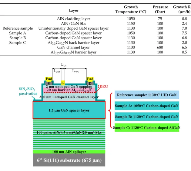
The epitaxial structure of this HEMT was grown on a 6-inch Si(111) substrate by using the MOCVD system. The buffer layer comprised a 100-nm-thick AlN cladding layer, followed by 100 periods of carbon-doped AlN/GaN (4.5-/20-nm-thick) superlattices (SLs). After the buffer layer was completed, a 1.3-µm-thick GaN spacer layer, 300-nm-thick undoped GaN channel layer, 25-nm-thick Al0.27Ga0.73N barrier layer, and 2-nm-thick undoped GaN capping layer were grown. An unintentionally doped (UID) GaN spacer layer for the Reference sample was grown at 1130˝C. Two intentionally doped GaN spacer layers were grown, one at 1050˝C for Sample A and the other at 1130˝C for Sample B, respectively. The growth temperature of Sample A was relatively low because the CBr4precursor requires a low temperature to incorporate carbon into GaN. Furthermore, a 1-µm-thick low-carbon-doped Al0.3Ga0.7N back barrier layer for Sample C was grown on the top of the SL structure as an alternative spacer design for low CC. The growth pressures of the cladding layer, spacer layer, and barrier layer were fixed in the range from 75 to 100 Torr (10 to 13 kPa). A high-purity GaN channel layer was grown at 1130˝C and 680 Torr (90 kPa). The growth parameters, namely the growth temperature, growth pressure, and growth rate, are listed in Table1.
Following the epitaxial growth, fabrication of the HEMT device began with mesa isolation through inductively coupled plasma reactive ion etching (ICP-RIE). The ohmic contacts of the source/drain electrodes were fabricated through photolithography and a lift-off process. A stacking metal system of Ti/Al/Ni/Au (20/120/25/100 nm) was evaporated through electron beam evaporation. After the stacking metal deposition, thermal annealing was employed at 850˝C to form the ohmic contact. The contact resistance of the source/drain electrodes was estimated to be 8.3 ˆ 10´5Ω-cm2(according to transmission line model measurements). A SiNx/SiO2(20/280 nm) passivation structure was then deposited through plasma-enhanced chemical vapor deposition (PECVD). A stacking metal system of Ni/Au (50/300 nm) was evaporated through electron beam evaporation to serve as the Schottky gate metal. The HEMT device was realized with a 2-µm gate length (LG), 5-µm source-to-gate distance (LSG), 5 to 20-µm gate-to-drain distance (LGD), and 500-µm gate width (WG), as presented in Figure1.
Electronics 2016, 5, 28 3 of 11
In addition, a two-terminal buffer layer BV test structure was fabricated on this HEMT structure, the source and drain electrodes of which were isolated by 150-nm-deep dry etching. The LSDvalues were defined as 5, 10, 15, and 20 µm.
Table 1. Growth parameters of the samples grown by metal-organic chemical vapor deposition (MOCVD).
Layer Temperature (Growth ˝C)
Pressure (Torr)
Growth Rate (µm/h)
AlN cladding layer 1050 75 0.8 AlN/GaN SLs 1150 100 2.4 Reference sample Unintentionally doped GaN spacer layer 1130 100 7.0 Sample A Carbon-doped GaN spacer layer 1050 100 7.5 Sample B Carbon-doped GaN spacer layer 1130 100 6.8 Sample C Al0.3Ga0.7N back barrier layer 1130 100 2.0
GaN channel layer 1130 680 6.5 Al0.27Ga0.73N barrier layer 1130 100 0.5
Electronics 2016, 5, 28; doi:10.3390/electronics5020028 www.mdpi.com/journal/electronics Table 1. Growth parameters of the samples grown by metal-organic chemical vapor deposition (MOCVD). Layer Growth Temperature (°C) Pressure (Torr) Growth Rate (µm/h)
AlN cladding layer 1050 75 0.8
AlN/GaN SLs 1150 100 2.4
Reference sample Unintentionally doped GaN spacer layer 1130 100 7.0 Sample A Carbon-doped GaN spacer layer 1050 100 7.5 Sample B Carbon-doped GaN spacer layer 1130 100 6.8 Sample C Al0.3Ga0.7N back barrier layer 1130 100 2.0
GaN channel layer 1130 680 6.5
Al0.27Ga0.73N barrier layer 1130 100 0.5
Following the epitaxial growth, fabrication of the HEMT device began with mesa isolation through inductively coupled plasma reactive ion etching (ICP-RIE). The ohmic contacts of the source/drain electrodes were fabricated through photolithography and a lift-off process. A stacking metal system of Ti/Al/Ni/Au (20/120/25/100 nm) was evaporated through electron beam evaporation. After the stacking metal deposition, thermal annealing was employed at 850 °C to form the ohmic contact. The contact resistance of the source/drain electrodes was estimated to be 8.3 × 10⁻⁵ Ω-cm2 (according to transmission line model measurements). A SiNx/SiO2 (20/280 nm) passivation structure was then deposited through plasma-enhanced chemical vapor deposition (PECVD). A stacking metal system of Ni/Au (50/300 nm) was evaporated through electron beam evaporation to serve as the Schottky gate metal. The HEMT device was realized with a 2-µm gate length (LG), 5-µm source-to-gate distance (LSG), 5 to 20-µm gate-to-drain distance (LGD), and 500-µm gate width (WG), as presented in Figure 1. In addition, a two-terminal buffer layer BV test structure was fabricated on this HEMT structure, the source and drain electrodes of which were isolated by 150-nm-deep dry etching. The LSD values were defined as 5, 10, 15, and 20 µm.
Figure 1. Cross-sectional diagram of an AlGaN/GaN HEMT. The spacer layers were fabricated at 1150 °C as UID GaN (Reference sample), at 1050 °C as carbon-doped GaN (Sample A), at 1130 °C as carbon-doped GaN (Sample B), and at 1130 °C as carbon-doped AlGaN (Sample C).
Figure 1. Cross-sectional diagram of an AlGaN/GaN HEMT. The spacer layers were fabricated at 1150˝C as UID GaN (Reference sample), at 1050˝C as carbon-doped GaN (Sample A), at 1130˝C as carbon-doped GaN (Sample B), and at 1130˝C as carbon-doped AlGaN (Sample C).
3. Results and Discussion
3.1. Strained SLs Buffer Layer of GaN-on-Si Epitaxy
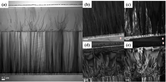
Figure2a shows bright field transmission electron microscope (TEM) cross-sectional images of the Reference sample with a UID GaN spacer layer. The figure shows TDs of extreme magnitude at the AlN/GaN SL structure. However, the threading dislocation density (TDD) gradually decreased from the carbon-doped AlN/GaN SL structure to the GaN spacer layer. To estimate the TDD, two-beam condition TEM images were captured to determine the TDD [18], as shown in Figure2b–e. The images in Figure2b,c were captured from the carbon-doped AlN/GaN SL region, and those in Figure2d,e were captured from the GaN spacer layer.
Electronics 2016, 5, 28 4 of 11
Electronics 2016, 5, 28; doi:10.3390/electronics5020028 www.mdpi.com/journal/electronics 3. Results and Discussion
3.1. Strained SLs Buffer Layer of GaN-on-Si Epitaxy
Figure 2a shows bright field transmission electron microscope (TEM) cross-sectional images of the Reference sample with a UID GaN spacer layer. The figure shows TDs of extreme magnitude at the AlN/GaN SL structure. However, the threading dislocation density (TDD) gradually decreased from the carbon-doped AlN/GaN SL structure to the GaN spacer layer. To estimate the TDD, two-beam condition TEM images were captured to determine the TDD [18], as shown in Figures 2b–e. The images in Figures 2b,c were captured from the carbon-doped AlN/GaN SL region, and those in Figures 2d,e were captured from the GaN spacer layer.
The total number of TDDs, including edge-type, screw-type, and mixed-type dislocations, were estimated to be higher than 1010 cm−2 at the region of the carbon-doped AlN/GaN SLs, falling to approximately 5.2 × 109 cm−2 at the region above the carbon-doped AlN/GaN SLs. The densities of the edge-type and mixed-type dislocations in the GaN spacer layer region were estimated to be 3.2 × 10⁹ and 2.0 × 109 cm−2, respectively. The density of the screw-type TDs was estimated to be less than 106 cm−2. The total number of TDDs in the GaN spacer layer region was approximately 5.2 × 109 cm−2. The low number of TDDs in the GaN spacer layer might be attributed to the AlN/GaN SLs controlling the stress. Masahiro Ishida et al. reported using SLs for stress control in GaN-on-Si epitaxial layers [19]. The total stress was discussed in terms of structural modeling, which considered lattice mismatch, misfit dislocation density, wafer curvature, and coefficient of thermal expansion. Furthermore, an SL stack composed of unreleased AlN and GaN layers with 1% strain release at each pair of SLs was demonstrated, which effectively controlled the compressive stress introduced during growth. Experiments showed that bowing and cracking can be eliminated by introducing SLs into GaN-on-Si epitaxial structures. This implies that TDs tend to release the compressive stress and that TDDs can be reduced. This design factor is crucial for strain control because a high number of TDDs will reduce the BV. Therefore, a GaN epilayer with a low number of TDDs can be grown without the necessary of a thick GaN buffer layer [5].
Figure 2. (a) Bright field cross-sectional TEM images with a zone axis where g = [11–20]; (b,c) show the TEM two-beam condition dark field images of carbon-doped AlN/GaN SLs with a zone axis, where g = [0002] and g = [1–100], respectively; (d,e) show the TEM two-beam condition images of the GaN spacer layer with a zone axis, where g = [0002] and g = [1–100], respectively.
Figure 2.(a) Bright field cross-sectional TEM images with a zone axis where g = [11–20]; (b,c) show the TEM two-beam condition dark field images of carbon-doped AlN/GaN SLs with a zone axis, where g = [0002] and g = [1–100], respectively; (d,e) show the TEM two-beam condition images of the GaN spacer layer with a zone axis, where g = [0002] and g = [1–100], respectively.
The total number of TDDs, including edge-type, screw-type, and mixed-type dislocations, were estimated to be higher than 1010cm´2at the region of the carbon-doped AlN/GaN SLs, falling to approximately 5.2 ˆ 109cm´2at the region above the carbon-doped AlN/GaN SLs. The densities of the edge-type and mixed-type dislocations in the GaN spacer layer region were estimated to be 3.2 ˆ 109and 2.0 ˆ 109cm´2, respectively. The density of the screw-type TDs was estimated to be less than 106cm´2. The total number of TDDs in the GaN spacer layer region was approximately 5.2 ˆ 109cm´2. The low number of TDDs in the GaN spacer layer might be attributed to the AlN/GaN SLs controlling the stress. Masahiro Ishida et al. reported using SLs for stress control in GaN-on-Si epitaxial layers [19]. The total stress was discussed in terms of structural modeling, which considered lattice mismatch, misfit dislocation density, wafer curvature, and coefficient of thermal expansion. Furthermore, an SL stack composed of unreleased AlN and GaN layers with 1% strain release at each pair of SLs was demonstrated, which effectively controlled the compressive stress introduced during growth. Experiments showed that bowing and cracking can be eliminated by introducing SLs into GaN-on-Si epitaxial structures. This implies that TDs tend to release the compressive stress and that TDDs can be reduced. This design factor is crucial for strain control because a high number of TDDs will reduce the BV. Therefore, a GaN epilayer with a low number of TDDs can be grown without the necessary of a thick GaN buffer layer [5].
3.2. Carbon-Doping Activities in GaN Spacer Layer
First, the relationship between the carbon-doping concentration and growth temperature of the GaN spacer layer was considered. In the growth stage, the flow rates of CBr4and TMG were fixed to ensure that uniform amounts of carbon adatoms were incorporated into the GaN. The V/III ratio was fixed at 3000, and nitrogen was used as the carrier gas at a flow rate of 1000 sccm for the CBr4precursor. A secondary ion mass spectroscopy (SIMS) depth profile was employed to determine the carbon-doping concentration of GaN spacer layer. The UID carbon-doping concentration of the Reference sample was less than 5 ˆ 1017cm´3, implying that the GaN grown under low-pressure conditions remained at a residual carbon-doping concentration. In contrast, the carbon-doping concentration of the GaN channel layer was measured at less than 1 ˆ 1016cm´3, which was near the detection limit of the SIMS instrument. This implies that the higher growth pressure effectively obtained high-purity GaN, which is consistent with previous studies [20]. Furthermore, the carbon-doping concentration depended
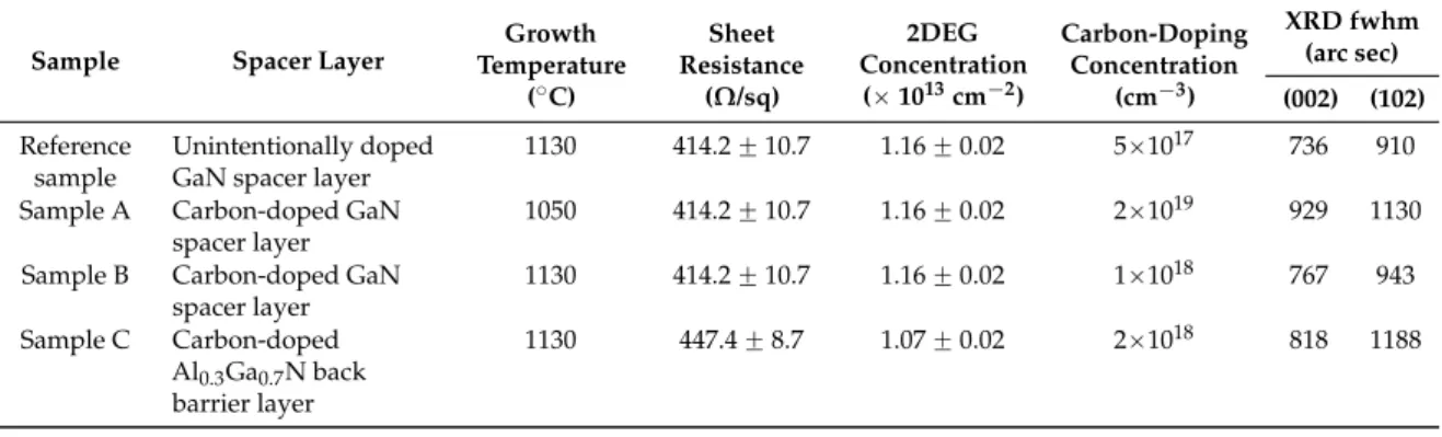
strongly on the growth temperature. Sample A was grown with its intentionally carbon-doped GaN spacer layer at 1050˝C and had a carbon-doping concentration of 2 ˆ 1019cm´3, whereas Sample B was grown at 1130˝C and had a carbon-doping concentration of 1 ˆ 1018cm´3. This implies that doping carbon into GaN at a very high growth temperature is infeasible. In [21], D. S. Green et al. also found that the substrate temperature will lead to a decreasing in carbon incorporation. Their investigation found a non-linear curve between carbon doping concentration and substrate temperature, which means that more than one process is responsible for the decline of carbon incorporation into GaN at higher temperatures. So far, the mechanism is still unclear due to its lack of more detailed studies, especially in growth of carbon-doped GaN by CBr4through MOCVD growth. Here, the AlGaN back barrier that was grown at a high temperature showed a low carbon-doping concentration of 2 ˆ 1018 cm´3. We anticipated that the low-carbon-doped AlGaN would serve as a back barrier that keeps lower carbon-induced traps but blocks electron leakage with its high bandgap. Table2 summarizes the structural characteristics of the samples with different carbon-doping concentrations in the spacer layers. The Hall measurements of the specimens were also investigated and shown in Table2. The results of the Reference sample, Sample A, and Sample B yielded an electron mobility of 1315 ˘ 25 cm2/V¨ s and a sheet resistance of 414.2 ˘ 10.7Ω/sq. The 2DEG concentration of Sample C is 1.07 ˘ 0.02 ˆ 1013 cm´2, which is lower than the value of our conventional HEMTs with GaN spacer. The lower 2DEG density is due to GaN channels potential being pulled up by the AlGaN spacer, which is similar to a previous report [22]. The raised potential also leads to a positive shift of threshold voltage, which will be discussed later in this paper. X-ray diffraction (XRD) results show that the full width at half maximum (FWHM) gradually increased with the carbon-doping concentration. This feature was attributed to higher carbon-doping concentrations requiring lower growth temperatures. The results indicate that the growth temperature exerts a remarkable effect on the crystalline quality of GaN. Moreover, the higher lattice mismatch between GaN and the AlGaN back barrier leads to a higher strain, which caused Sample C to return an unusually broad FWHM. An AlGaN back barrier yielded slightly lower crystalline quality than that of a high carbon-doped GaN spacer. This result is very encouraging, because a high-quality AlGaN epilayer could markedly alter a device’s electrical performance through its carbon-doping regime, particularly by reducing the channel of substrate leakage for high-power HEMT devices.
Table 2.Summary of the structural characteristics of the samples.
Sample Spacer Layer TemperatureGrowth (˝C) Sheet Resistance (Ω/sq) 2DEG Concentration (ˆ 1013cm´2) Carbon-Doping Concentration (cm´3) XRD fwhm (arc sec) (002) (102) Reference sample Unintentionally doped GaN spacer layer
1130 414.2 ˘ 10.7 1.16 ˘ 0.02 5ˆ1017 736 910 Sample A Carbon-doped GaN
spacer layer
1050 414.2 ˘ 10.7 1.16 ˘ 0.02 2ˆ1019 929 1130 Sample B Carbon-doped GaN
spacer layer 1130 414.2 ˘ 10.7 1.16 ˘ 0.02 1ˆ1018 767 943 Sample C Carbon-doped Al0.3Ga0.7N back barrier layer 1130 447.4 ˘ 8.7 1.07 ˘ 0.02 2ˆ1018 818 1188
3.3. Breakdown Voltage Discussion
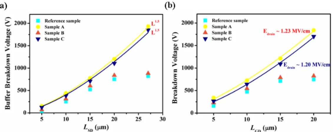
In this section, we discuss the BV improvement from the carbon-doped GaN spacer layer. The SI GaN spacer layer is responsible for blocking electron leakage punchthrough from channel to substrate when a high voltage is supplied. The two-terminal BV is defined as the supplied voltage for leakage currents up to 10 µA/mm. As shown in Figure3a, the buffer BVs of the Reference sample and Sample B saturate at approximately 800 V when the LSDis larger than 15 µm. This means that the buffer leakage is severe because these samples exhibit low resistivity of the buffer layers due to lower carbon-doping concentrations. The BV shows strong dependence on the carbon-doping concentration in the GaN
spacer layer, except for Sample C. The carbon-doping concentration of Sample C was not higher than that of Sample A, but the high bandgap of the AlGaN back barrier blocks electron leakage to the substrate. Therefore, we could obtain a comparable BV even if a sample was grown at an excessively high temperature with inefficient carbon incorporation into the AlGaN. This is crucial because we expected that a higher growth temperature would reduce the number of buffer traps, leading to improvements regarding the CC phenomenon. Furthermore, the buffer BV could be functionally fitted to LSD, which could extract the dominant mechanism of the BV for a HEMT device. The fitting results of Sample A and Sample C suggest that the BV is proportionate to LSD, because BV « L1.5SDfor both samples, with R2values of 0.99. This dependence implies that space-charge-limited (SCL) transport [23] is present in the leakage current. According to a previous study [2], SCL transport theory implies that the supplied voltage between the source and drain can be expressed as V “a8J{9εµL1.5SD, where ε and µare the dielectric constant and effective carrier mobility including the trapping effect, respectively. The leakage is denoted as J. However, the SCL transport of our devices was investigated through three-terminal device measurements to confirm the presence of SCL transports in these devices.
Electronics 2016, 5, 28 7 of 12
Electronics 2016, 5, 28; doi:10.3390/electronics5020028 www.mdpi.com/journal/electronics obtain the electric field at the drain electrode by Edrain = 2(LGD A)+Ein2 [2]. At a 20-µm distance, the electric fields of LGD at the drain electrode are between 1.23 and 1.20 MV/cm for Sample A and Sample C, respectively. These electric fields are substantially smaller than the critical electric field of GaN, implying that the BVs of our devices are not limited by impact ionization—even the high-resistivity buffer layer was inserted [2].
Figure 3. (a) Two-terminal buffer BV vs. LSD for HEMT samples. (b) Three-terminal BV vs. LGD for HEMT samples. The BV was captured for leakage currents up to 10 ìA/mm with different distances between pads.
3.4. HEMT Electrical Properties
The performance of the HEMT devices was characterized through an electrical analysis. Figure 4a shows the transfer characteristics of the devices. The subthreshold drain leakage current at the off-state is more than one and a half orders of magnitude lower in Sample C with the AlGaN back barrier, as compared with the Reference sample with the UID GaN spacer. This current was attributed to the reverse bias Schottky contact of the gate, which means that the lower buffer leakage was obtained in Sample C. Sample A shows the lowest off-state subthreshold drain leakage current due to its highest carbon-doping concentration into the GaN spacer, which is consistent with the BV results. In addition, the threshold voltage was shifted from −4.62 V to −4.35 V, which is related to the lower density of 2DEG [22]. However, the hysteresis IDS–VGS curves of the Reference sample and Sample C are shown in the inset of Figure 4a, respectively. We can observe that a larger positive shift of the hysteresis IDS–VGS curve in the Reference sample, which implies that a higher trap density leads to the transient phenomenon in the Reference sample but we can not conclude what kind of the traps. Figure 4b shows the on-state IDS–VDS characteristics for Sample A and Sample C. Both specimens had LG/LGD = 2/20 µm. At VGS = 0 V, the IDS,max reached 240 and 215 mA/mm for Sample A and Sample C, respectively. From the previous results, the specific on-state resistance (spec. Ron) at VGS = 0 V was 5.1 mΩ-cm2 for Sample A and 7.2 mΩ-cm2 for Sample C. The smaller drain current in the device with the back barrier resulted from the lower density of 2DEG and the subsequent higher threshold voltage. Therefore, the higher sheet resistance will lead to a higher on-resistance for the HEMT with the AlGaN back barrier [24]. To investigate the relationship between the carbon-doped buffer layer and the CC phenomenon, the dynamic on-state resistance is discussed. Hot electrons can overcome the energy barrier and thereby escape from the 2DEG channel, but subsequently become trapped by defects [25,26]. Such defects come not only from surface states, but also from intrinsic defects (e.g., TDs, VN). Trapping electrons on
Figure 3.(a) Two-terminal buffer BV vs. LSDfor HEMT samples. (b) Three-terminal BV vs. LGDfor HEMT samples. The BV was captured for leakage currents up to 10 ìA/mm with different distances between pads.
The three-terminal off-state BV was defined as VDSat IDSequal to 10 µA/mm with VGS= ´10 V. Sample A, with a higher carbon-doping concentration in the spacer layer, demonstrated a high BV of 1839 V. Considering Sample A, Sample B, and the Reference sample, the BV gradually diminished as the carbon-doping concentration decreased in the spacer layer. This is consistent with our previous discussion of the two-terminal BV measurement result, which was attributed to the improvement in buffer layer isolation. Furthermore, Sample C shows a BV that is higher than 1702 V with an AlGaN back barrier. The electric field at the Schottky gate contact is considered to explain the SCL transport model. The comparison of the BV vs. LGD could be functionally fitted as VDS „ VDG “ A
„b
p2LGD{A ` Ein2q1.5´E3in
{3, where A = µε{J = 0.00579 to 0.00627 µm3{V2, and Einis the electric field at the gate electrode. By means of Einand A, we could obtain the electric field at the drain electrode by Edrain“
b
2pLGD{Aq ` Ein2 [2]. At a 20-µm distance, the electric fields of LGDat the drain electrode are between 1.23 and 1.20 MV/cm for Sample A and Sample C, respectively. These electric fields are substantially smaller than the critical electric field of GaN, implying that the BVs of our devices are not limited by impact ionization—even the high-resistivity buffer layer was inserted [2].
3.4. HEMT Electrical Properties
The performance of the HEMT devices was characterized through an electrical analysis. Figure4a shows the transfer characteristics of the devices. The subthreshold drain leakage current at the off-state is more than one and a half orders of magnitude lower in Sample C with the AlGaN back barrier, as compared with the Reference sample with the UID GaN spacer. This current was attributed to the reverse bias Schottky contact of the gate, which means that the lower buffer leakage was obtained in Sample C. Sample A shows the lowest off-state subthreshold drain leakage current due to its highest carbon-doping concentration into the GaN spacer, which is consistent with the BV results. In addition, the threshold voltage was shifted from ´4.62 V to ´4.35 V, which is related to the lower density of 2DEG [22]. However, the hysteresis IDS–VGScurves of the Reference sample and Sample C are shown in the inset of Figure4a, respectively. We can observe that a larger positive shift of the hysteresis IDS–VGScurve in the Reference sample, which implies that a higher trap density leads to the transient phenomenon in the Reference sample but we can not conclude what kind of the traps. Figure4b shows the on-state IDS–VDScharacteristics for Sample A and Sample C. Both specimens had LG/LGD= 2/20 µm. At VGS= 0 V, the IDS,maxreached 240 and 215 mA/mm for Sample A and Sample C, respectively. From the previous results, the specific on-state resistance (spec. Ron) at VGS = 0 V was 5.1 mΩ-cm2for Sample A and 7.2 mΩ-cm2for Sample C. The smaller drain current in the device with the back barrier resulted from the lower density of 2DEG and the subsequent higher threshold voltage. Therefore, the higher sheet resistance will lead to a higher on-resistance for the HEMT with the AlGaN back barrier [24]. To investigate the relationship between the carbon-doped buffer layer and the CC phenomenon, the dynamic on-state resistance is discussed. Hot electrons can overcome the energy barrier and thereby escape from the 2DEG channel, but subsequently become trapped by defects [25,26]. Such defects come not only from surface states, but also from intrinsic defects (e.g., TDs, VN). Trapping electrons on the surface would deplete the channel carrier concentration, resulting in a virtual gate as well as a reduction in the drain current [27,28]. Although the trapping at the surface or inside the AlGaN barrier layer is crucial to CC, the electrons trapped in the GaN buffer by charging/discharging from deep traps are also responsible for CC. As shown in Figure4c,d, the CC phenomenon was clearly observed in both Sample A and Sample C. Pulsed IDS–VDScharacteristics were extracted from the off-state with a quiescent gate bias (VGSQ) of ´5 V to an on-state at 0 V in 500 ns and a separation of 1 ms. The quiescent drain bias (VDSQ) was swept from 0 to 40 V (in 10 V increments). The dynamic on-resistance of Sample A increased from 5.1 mΩ-cm2to 12.68 mΩ-cm2as the VDSQwas swept from 0 to 40 V. In contrast, the dynamic on-resistance of Sample C increased from 7.2 mΩ-cm2to 14.44 mΩ-cm2. The dispersion of dynamic on-resistance for Sample A is 2.48 times that for the static state but 2.00 times that for Sample C, a smaller dispersion between VDSQ= 0 to 40 V was obtained from Sample C. Both Sample A and Sample C were passivated by the same SiNx/SiO2 (20/280 nm) layers; hence, the surface trap-induced CC was improved and the dynamic on-resistance was in the same situation. Here, the dynamic on-resistances show different dispersions, implying that another cause led to CC. Therefore, the pulsed IDS–VDScharacteristic cannot clearly identify the location of traps in HEMT structures because the electrons are trapped not only by buffer traps, but also by surface traps under relatively high stress [28]. Therefore, we require another measurement to investigate the location of the traps.
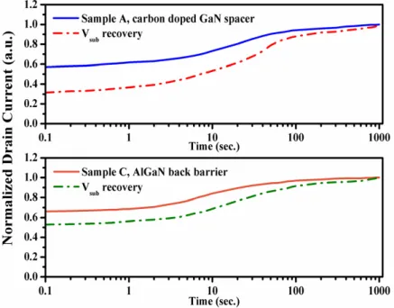
Because it is difficult to verify whether CC has been induced by surface traps or buffer layers, pulsed IDtransients were captured for Sample A and Sample C. Figure5shows CC recovery versus device conductance as a function of stress time. The measurement started with the device in the off-state at VGS= ´5 V and a VDSof 50 V; the device was left in the off-state for 1000 s, after which the HEMT was pulsed back to the on-state (linear region) of VGS= 0 V, VDS= 1 V for 10 ms; measurements were performed of the drain current and IDas functions of time (1000 s). Sample C showed a relatively small change compared with Sample A, which was consistent with dynamic on-resistance measurements. The results imply that there were traps in these HEMT structures, but the information was insufficient for clearly identifying the trap locations. Next, a VSUBof ´200 V was supplied, and pulsed IDtransient
Electronics 2016, 5, 28 8 of 11
currents were recorded, as shown in Figure5(dashed lines). The substrate bias provided an electric field and then attracted electrons from the channels to the buffer traps. The pulsed IDtransient current with substrate bias is a favorable analysis method for identifying buffer traps, but it also shows the differences between two kinds of specimens [29]. The larger dispersion of IDtransient current for Sample A implies that the buffer trap-induced CC will lead to a gradual change in the IDtransient current [12,28,29]; that slow change is related to all defects associated with the low-temperature growth of carbon-doped GaN spacer layers. In contrast, a low-carbon-doped AlGaN back barrier was grown at a higher temperature, leading to fewer traps and obtaining low dispersion in the IDtransient current under substrate bias. This result implies that the buffer traps affecting the CC behaviors of GaN-on-Si HEMTs may result from incorporating carbon into GaN to isolate the channel from substrate leakage at high electric fields.
Electronics 2016, 5, 28; doi:10.3390/electronics5020028 www.mdpi.com/journal/electronics
the surface would deplete the channel carrier concentration, resulting in a virtual gate as well as a reduction in the drain current [27,28]. Although the trapping at the surface or inside the AlGaN barrier layer is crucial to CC, the electrons trapped in the GaN buffer by charging/discharging from deep traps are also responsible for CC. As shown in Figures 4c,d, the CC phenomenon was
clearly observed in both Sample A and Sample C. Pulsed IDS–VDS characteristics were extracted
from the off-state with a quiescent gate bias (VGSQ) of −5 V to an on-state at 0 V in 500 ns and a
separation of 1 ms. The quiescent drain bias (VDSQ) was swept from 0 to 40 V (in 10 V increments).
The dynamic on-resistance of Sample A increased from 5.1 mΩ-cm2 to 12.68 mΩ-cm2 as the VDSQ
was swept from 0 to 40 V. In contrast, the dynamic on-resistance of Sample C increased from 7.2
mΩ-cm2 to 14.44 mΩ-cm2. The dispersion of dynamic on-resistance for Sample A is 2.48 times that
for the static state but 2.00 times that for Sample C, a smaller dispersion between VDSQ = 0 to 40 V
was obtained from Sample C. Both Sample A and Sample C were passivated by the same
SiNx/SiO2 (20/280 nm) layers; hence, the surface trap-induced CC was improved and the dynamic
on-resistance was in the same situation. Here, the dynamic on-resistances show different
dispersions, implying that another cause led to CC. Therefore, the pulsed IDS–VDS characteristic
cannot clearly identify the location of traps in HEMT structures because the electrons are trapped not only by buffer traps, but also by surface traps under relatively high stress [28]. Therefore, we require another measurement to investigate the location of the traps.
Figure 4. (a) DC IDS–VGS characteristics for all specimens. The hysteresis IDS–VGS curves for the Reference sample and Sample C are shown in the inset. (b) DC IDS–VDS characteristics for Sample A and Sample C. Pulsed IDS–VDS characteristics for (c) Sample A and (d) Sample C. Pulsed IDS–VDS characteristics were extracted from a quiescent gate bias (VGSQ) of −5 V to an on-state at 0 V in 500 ns and a separation of 1 ms. Afterward, the quiescent drain bias (VDSQ) was swept from 0 to 40 V (in 10-V increments).
Figure 4. (a) DC IDS–VGScharacteristics for all specimens. The hysteresis IDS–VGS curves for the Reference sample and Sample C are shown in the inset. (b) DC IDS–VDScharacteristics for Sample A and Sample C. Pulsed IDS–VDScharacteristics for (c) Sample A and (d) Sample C. Pulsed IDS–VDS characteristics were extracted from a quiescent gate bias (VGSQ) of ´5 V to an on-state at 0 V in 500 ns and a separation of 1 ms. Afterward, the quiescent drain bias (VDSQ) was swept from 0 to 40 V (in 10-V increments).
Poor crystal quality is the most critical drawback of GaN-on-Si HEMTs. Heterostructures grown on Si substrates contain very high numbers of TDs and produce defects because of the high lattice mismatch. Those defects act as deep traps on the GaN surface or in the buffer layers. Some unexpected effects, such as the vertical leakage, reduction in BV, and CC, are strongly presumed to be related to those defects [30,31]. Electrons captured in or escaping from those traps result in destructive phenomena because of the charging/discharging activities in those traps. In this research, a low-carbon-doped AlGaN back barrier was employed to instead of a high-carbon-doped GaN spacer layer. The results show that the BV for an HEMT with an AlGaN back barrier is comparable to
Electronics 2016, 5, 28 9 of 11
that for a device with a conventional carbon-doped GaN spacer layer. Although the carbon-doping concentration of the AlGaN back barrier was less than that of a carbon-doped GaN spacer layer, the higher bandgap of AlGaN provides an effective barrier for blocking current leakage from the channel to the substrate. The most crucial point is that an AlGaN back barrier that has been grown at a high temperature shows a lower dispersion of pulsed IDtransient current under substrate bias, which means that the buffer traps are effectively suppressed. Therefore, we obtained a lower dynamic on-resistance by using AlGaN back barriers in the HEMTs. These two approaches improve device performance and provide an effective and easy means for preventing undesirable phenomena and producing reliable devices for high-power applications.
Electronics 2016, 5, 28; doi:10.3390/electronics5020028 www.mdpi.com/journal/electronics
Because it is difficult to verify whether CC has been induced by surface traps or buffer layers,
pulsed I
Dtransients were captured for Sample A and Sample C. Figure 5 shows CC recovery versus
device conductance as a function of stress time. The measurement started with the device in the
off-state at V
GS= −5 V and a V
DSof 50 V; the device was left in the off-state for 1000 s, after which the
HEMT was pulsed back to the on-state (linear region) of V
GS= 0 V, V
DS= 1 V for 10 ms;
measurements were performed of the drain current and I
Das functions of time (1000 s). Sample C
showed a relatively small change compared with Sample A, which was consistent with dynamic
on-resistance measurements. The results imply that there were traps in these HEMT structures, but
the information was insufficient for clearly identifying the trap locations. Next, a V
SUBof −200 V
was supplied, and pulsed I
Dtransient currents were recorded, as shown in Figure 5 (dashed lines).
The substrate bias provided an electric field and then attracted electrons from the channels to the
buffer traps. The pulsed I
Dtransient current with substrate bias is a favorable analysis method for
identifying buffer traps, but it also shows the differences between two kinds of specimens [29].
The larger dispersion of I
Dtransient current for Sample A implies that the buffer trap-induced CC
will lead to a gradual change in the I
Dtransient current [12,28,29]; that slow change is related to all
defects associated with the low-temperature growth of carbon-doped GaN spacer layers. In
contrast, a low-carbon-doped AlGaN back barrier was grown at a higher temperature, leading to
fewer traps and obtaining low dispersion in the I
Dtransient current under substrate bias. This
result implies that the buffer traps affecting the CC behaviors of GaN-on-Si HEMTs may result
from incorporating carbon into GaN to isolate the channel from substrate leakage at high electric
fields.
Figure 5. Normalized current recovery of device conductance as a function of time. The solid lines
show the pulsed ID transient currents. The dashed lines show conductance recovery after
supplying a substrate bias of VSUB = −200 V.
Poor crystal quality is the most critical drawback of GaN-on-Si HEMTs. Heterostructures
grown on Si substrates contain very high numbers of TDs and produce defects because of the high
lattice mismatch. Those defects act as deep traps on the GaN surface or in the buffer layers. Some
unexpected effects, such as the vertical leakage, reduction in BV, and CC, are strongly presumed to
be related to those defects [30,31]. Electrons captured in or escaping from those traps result in
destructive phenomena because of the charging/discharging activities in those traps. In this
research, a low-carbon-doped AlGaN back barrier was employed to instead of a
Figure 5.Normalized current recovery of device conductance as a function of time. The solid lines show the pulsed IDtransient currents. The dashed lines show conductance recovery after supplying a substrate bias of VSUB= ´200 V.
4. Conclusions
We demonstrated the structural design of a GaN-on-Si HEMT with a high BV and low CC. The structural analysis shows that the strain and TDD were well-controlled through AlN/GaN SLs. An alternative AlGaN back barrier was grown at a high temperature and with a low carbon-doping concentration but with high crystal quality. The BV of the GaN-on-Si HEMT with the AlGaN back barrier was 1702 V, which is comparable to the BV of regular HEMTs with carbon-doped GaN spacer layers. The pulsed ID–VD characteristics of our devices show low dynamic on-resistance, which correlated with improved crystal quality. A low dispersion of transiently pulsed IDwas observed under substrate bias, which means that the buffer traps were effectively suppressed by the AlGaN back barrier grown at a high temperature. The two features of the AlGaN back barrier lead to a high BV and low CC. The reported method is a very simple and effective ways for fabricating high-BV GaN-on-Si HEMTs for high-power applications.
Acknowledgments: This study was funded by the Ministry of Science and Technology of Republic of China under grant number MOST 104-3113-E-009-002-CC2.
Author Contributions:An-Jye Tzou, Szu-Hung Chen, Yu-Kuang Liao, Chun-Yen Chang, and Hao-Chung Kuo discussed the topic. Zhen-Yu Li fabricated the different devices and performed the measurements. All authors discussed the data analysis and interpretation, and contributed equally to the writing of the manuscript. All authors approve the final version of the manuscript.
Conflicts of Interest:The authors declare no conflict of interest.
References
1. Mitova, R.; Ghosh, R.; Mhaskar, U.; Klikic, D.; Wang, M.X.; Dentella, A. Investigations of 600-V GaN HEMT and GaN Diode for Power Converter Applications. IEEE Trans. Power Electron. 2014, 29, 2441–2452. [CrossRef]
2. Lu, B.; Palacios, T. High Breakdown (>1500 V) AlGaN/GaN HEMTs by Substrate-Transfer Technology. IEEE Electron. Dev. Lett. 2010, 31, 951–953. [CrossRef]
3. Seager, C.H.; Wright, A.F.; Yu, J.; Götz, W. Role of carbon in GaN. J. Appl. Phys. 2002, 92, 6553–6560. [CrossRef]
4. Shan, Q.F.; Meyaard, D.S.; Dai, Q.; Cho, J.; Schubert, E.F.; Son, J.K.; Sone, C. Transport-mechanism analysis of the reverse leakage current in GaInN light-emitting diodes. Appl. Phys. Lett. 2011, 99, 253506. [CrossRef] 5. Selvaraj, S.L.; Watanabe, A.; Wakejima, A.; Egawa, T. 1.4-kV Breakdown Voltage for AlGaN/GaN
High-Electron-Mobility Transistors on Silicon Substrate. IEEE Electron. Dev. Lett. 2012, 33, 1375–1377. [CrossRef]
6. Srivastava, P.; Das, J.; Visalli, D.; Hove, M.V.; Malinowski, P.E.; Marcon, D.; Lenci, S.; Geens, K.; Cheng, K.; Leys, M.; et al. Record Breakdown Voltage (2200 V) of GaN DHFETs on Si With 2-µm Buffer Thickness by Local Substrate Removal. IEEE Electron. Dev. Lett. 2011, 32, 30–32. [CrossRef]
7. Jiang, Q.; Liu, C.; Lu, Y.; Chen, K.J. Mechanism of PEALD-grown AlN passivation for AlGaN/GaN HEMTs: Compensation of interface traps by polarization charges. IEEE Electron. Dev. Lett. 2013, 34, 357–359. [CrossRef]
8. Treidel, E.B.; Brunner, F.; Hilt, O.; Cho, E.; Würfl, J.; Tränkle, G. AlGaN/GaN/GaN:C Back-Barrier HFETs with Breakdown Voltage of Over 1 kV and Low RonˆA. IEEE Trans. Electron. Dev. 2010, 57, 3050–3058. [CrossRef]
9. Xuan, R.; Kuo, W.H.; Hu, C.W.; Lin, S.F.; Chen, J.F. Enhancing threshold voltage of AlGaN/GaN high electron mobility transistors by nano rod structure: From depletion mode to enhancement mode. Appl. Phys. Lett. 2012, 101, 112105. [CrossRef]
10. Koleske, D.D.; Wickenden, A.E.; Henry, R.L.; Twigg, M.E. Influence of MOVPE growth conditions on carbon and silicon concentrations in GaN. J. Cryst. Growth 2002, 242, 55–69. [CrossRef]
11. Poblenz, C.; Waltereit, P.; Rajan, S.; Heikman, S.; Mishra, U.K.; Speck, J.S. Effect of carbon doping on buffer leakage in AlGaN/GaN high electron mobility transistors. J. Vac. Sci. Technol. B 2004, 22, 1145–1149. [CrossRef]
12. Zhou, C.; Jiang, Q.; Huang, S.; Chen, K.J. Vertical Leakage/Breakdown Mechanisms in AlGaN/GaN-on-Si Devices. IEEE Electron. Dev. Lett. 2012, 33, 1132–1134. [CrossRef]
13. Fang, Z.Q.; Claflin, B.; Look, D.C.; Green, D.S.; Vetury, R. Deep traps in AlGaN/GaN heterostructures studied by deep level transient spectroscopy: Effect of carbon concentration in GaN buffer layers. J. Appl. Phys. 2010, 108, 063706. [CrossRef]
14. Selvaraj, J.; Selvaraj, S.L.; Egawa, T. Effect of GaN Buffer Layer Growth Pressure on the Device Characteristics of AlGaN/GaN High-Electron-Mobility Transistors on Si. Jpn. J. Appl. Phys. 2009, 48, 121002. [CrossRef] 15. Uren, M.J.; Möreke, J.; Martin, K. Buffer Design to Minimize Current Collapse in GaN/AlGaN HFETs.
IEEE Trans. Electron. Dev. 2012, 59, 3327–3333. [CrossRef]
16. Uren, M.J.; Nash, K.J.; Balmer, R.S.; Martin, T.; Morvan, E.; Caillas, N.; Delage, S.L.; Ducatteau, D.; Grimbert, B.; de Jaeger, J.C. Punchthrough in short-channel AlGaN/GaN HFETs. IEEE Trans. Electron. Dev. 2006, 53, 395–398. [CrossRef]
17. Zhang, L.; Lester, L.F.; Baca, A.G.; Shul, R.J.; Chang, P.C.; Willison, C.G.; Mishra, U.K.; Denbaars, S.P.; Zolper, J.C. Epitaxially-grown GaN junction field effect transistors. IEEE Trans. Electron. Dev. 2000, 47, 507–511. [CrossRef]
18. Heying, B.; Wu, X.H.; Keller, S.; Li, Y.; Kapolnek, D.; Keller, B.P. Role of threading dislocation structure on the X-ray diffraction peak widths in epitaxial GaN films. Appl. Phys. Lett. 1996, 68, 643–645. [CrossRef] 19. Ishida, M.; Ueda, T.; Ueda, D. GaN on Si Technologies for Power Switching Devices. IEEE Trans. Electron Dev.
20. Kim, D.S.; Won, C.H.; Kang, H.S.; Kim, Y.J.; Kim, Y.T.; Kang, I.M.; Lee, J.H. Growth and characterization of semiinsulating carbon-doped/undoped GaN multiple-layer buffer. Semicond. Sci. Technol. 2015, 30, 035010. [CrossRef]
21. Green, D.S.; Mishra, U.K.; Speck, J.S. Carbon doping of GaN with CBr4 in radio-frequency plasma-assisted molecular beam epitaxy. J. Appl. Phys. 2004, 95, 8456–8462. [CrossRef]
22. Liu, J.; Zhou, Y.; Zhu, J.; Lau, K.M.; Chen, K.J. AlGaN/GaN/InGaN/GaN DH-HEMTs with an InGaN Notch for Enhanced Carrier Confinement. IEEE Electron. Dev. Lett. 2006, 27, 10–12.
23. Lampert, M.A. Simplified theory of space-charge-limited currents in an insulator with traps. Phys. Rev. 1956, 103, 1648–1656. [CrossRef]
24. Lee, H.S.; Piedra, D.; Sun, M.; Gao, X.; Guo, S.; Palacios, T. 3000-V 4.3-mΩ¨ cm2 InAlN/GaN MOSHEMTs with AlGaN Back Barrier. IEEE Electron. Dev. Lett. 2012, 33, 982–984. [CrossRef]
25. Kim, H.; Tilak, V.; Green, B.M.; Smart, J.A.; Schaff, W.J.; Shealy, J.R.; Eastman, L.F. Reliability evaluation of high power AlGaN/GaN HEMTs on SiC substrate. Phys. Stat. Sol. 2001, 188, 203–206. [CrossRef]
26. Joh, J.; del Alamo, J.A. Impact of electrical degradation on trapping characteristics of GaN high electron mobility transistors. IEDM Tech. Dig. 2008, 1–4.
27. Vetury, R.; Zhang, N.Q.; Keller, S.; Mishra, U.K. The impact of surface states on the DC and RF characteristics of AlGaN/GaN HFETs. IEEE Trans. Electron Dev. 2001, 48, 560–566. [CrossRef]
28. Joh, J.; del Alamo, J.A. A Current-Transient Methodology for Trap Analysis for GaN High Electron Mobility Transistors. IEEE Trans. Electron. Dev. 2011, 58, 132–140. [CrossRef]
29. Uren, M.J.; Silvestri, M.; Cäsar, M.; Hurkx, G.A.M.; Croon, J.A.; Šonský, J.; Kuball, M. Intentionally Carbon-Doped AlGaN/GaN HEMTs: Necessity for Vertical Leakage Paths. IEEE Electron. Dev. Lett. 2014, 35, 327–329. [CrossRef]
30. Wolter, M.; Marso, M.; Javorka, P.; Bernát, J.; Carius, R.; Lüth, H.; Kordoš, P. Investigation of traps in AlGaN/GaN HEMTs on silicon substrate. Phys. Stat. Sol. 2003, 0, 2360–2363. [CrossRef]
31. Tirado, J.M.; Sanchez-Rojas, J.L.; Izpura, J.I. Simulation of surface state effects in the transient response of AlGaN/GaN HEMT and GaN MESFET devices. Semicond. Sci. Technol. 2006, 21, 1150–1159. [CrossRef]
© 2016 by the authors; licensee MDPI, Basel, Switzerland. This article is an open access article distributed under the terms and conditions of the Creative Commons Attribution (CC-BY) license (http://creativecommons.org/licenses/by/4.0/).