Instrument for x-ray absorption spectroscopy with in situ electrical control
characterizations
Chun-Chao Huang, Shu-Jui Chang, Chao-Yao Yang, Hsiung Chou, and Yuan-Chieh Tseng
Citation: Review of Scientific Instruments 84, 123904 (2013); doi: 10.1063/1.4849635 View online: http://dx.doi.org/10.1063/1.4849635
View Table of Contents: http://scitation.aip.org/content/aip/journal/rsi/84/12?ver=pdfcov Published by the AIP Publishing
Articles you may be interested in
Reaction cell for in situ soft x-ray absorption spectroscopy and resonant inelastic x-ray scattering measurements of heterogeneous catalysis up to 1 atm and 250°C
Rev. Sci. Instrum. 84, 113107 (2013); 10.1063/1.4829630
Design of a continuous-flow reactor for in situ x-ray absorption spectroscopy of solids in supercritical fluids Rev. Sci. Instrum. 83, 054101 (2012); 10.1063/1.4719921
Facility for combined in situ magnetron sputtering and soft x-ray magnetic circular dichroism Rev. Sci. Instrum. 77, 073903 (2006); 10.1063/1.2219719
An in situ cell for characterization of solids by soft x-ray absorption Rev. Sci. Instrum. 75, 3242 (2004); 10.1063/1.1791320
In situ x-ray absorption fuel cell
Instrument for x-ray absorption spectroscopy with
in situ
electrical
control characterizations
Chun-Chao Huang,1Shu-Jui Chang,1Chao-Yao Yang,1Hsiung Chou,2
and Yuan-Chieh Tseng1,a)
1Department of Materials Science and Engineering, National Chiao Tung University, Hsinchu, Taiwan 2Department of Physics, National Sun Yat-sen University, Kaohsiung, Taiwan
(Received 22 October 2013; accepted 3 December 2013; published online 20 December 2013) We report a synchrotron-based setup capable of performing x-ray absorption spectroscopy and x-ray magnetic circular dichroism with simultaneous electrical control characterizations. The setup can en-able research concerning electrical transport, element- and orbital-selective magnetization with an in situ fashion. It is a unique approach to the real-time change of spin-polarized electronic state of a material/device exhibiting magneto-electric responses. The performance of the setup was tested by probing the spin-polarized states of cobalt and oxygen of Zn1-xCoxO dilute magnetic
semi-conductor under applied voltages, both at low (∼20 K) and room temperatures, and signal vari-ations upon the change of applied voltage were clearly detected. © 2013 AIP Publishing LLC. [http://dx.doi.org/10.1063/1.4849635]
I. INTRODUCTION
Spintronics is an emerging technology exploiting the in-trinsic spin of the electron within solid-state devices. Tak-ing advantage of the spin degree of freedom of the electron we are able to store and transfer information in addition to the electron charge, such as magnetic semiconductors,1–3 gi-ant magnetoresistance (GMR), and tunnel magnetoresistance (TMR) devices.4–6 Understanding the interplays between the electrical and the magnetic responses of the devices is essen-tial to the spintronic technology. To make control of magne-tization fully compatible with current semiconductor devices, using an electric field to control magnetization is desired. Re-cently, studies of electrically controllable magnetic properties are a subject of intensive research.7–11These findings demon-strate the advances in spintronics because of possible device operation with reduced power consumption and the compat-ibility of electrically controlled devices with semiconductor integrated circuits. In a broader vision, the phenomenon in-cludes the electrically controlled magnetic ordering,12,13 ex-change bias,14–16spin transport,17–21and magneto-crystalline anisotropy (MCA).22–24
Although the findings are recognized as a great excite-ment, the underlying physics is rather elusive, especially from the viewpoint of electronic interactions. This is because most of these studies used polar Kerr effect coupled with electri-cal transport measurements, so the understanding of the elec-trically controlled properties is limited to a macroscopic vi-sion. The electronic interactions, the critical ingredient that governs the macroscopic response, have not been visualized by any conventional approaches so far. A general explanation for the phenomena is the change in the occupation of ferro-magnetic 3d orbital due to the band-filling effect.9–11 Such explanation was first proposed by Kyuno et al.25 who
theo-a)Author to whom correspondence should be addressed. Electronic mail: [email protected]
retically demonstrated that, the ferromagnetism (FM) order-ings of transition metals exhibit high sensitivity to 3d electron filling. Theoretical studies using first principle and density-functional calculations in recent years26–29 showed that the magnetocrystalline anisotropy (MCA) can be controlled by an electric field through the change of band structure, which hold a same picture as that of Kyuno et al.25 Despite in-tensive studies in the field, evidences of the electric-field induced change in spin-polarized electronic states have not been experimentally observed. This makes it difficult to vali-date the hypothesis of the band-filling effects.25–28Therefore, an instrument sensitive to the real-time change of electronic state with respect to the magnetic and transport response is very necessary to improve current understanding of the phenomenon.
In this article, we report on the development of a setup featuring in situ electrical and x-ray absorption characteriza-tion (defined as the E-X setup henceforth). For x-ray part, x-ray absorption spectroscopy (XAS) is a powerful tech-nique for probing the density of states (DOS) in the vicinity of the Fermi level. It is capable of studying the chemi-cal and physichemi-cal states of selected atomic species associ-ated with their electronic structures.30 X-ray magnetic circu-lar dichroism (XMCD)31gained from the difference of XAS with opposite x-ray helicities is especially suitable for prob-ing ferromagnetism, or materials with non-zero net mag-netization such as ferrimagnetism or canted antiferromag-netism. Therefore, the combination of XAS and XMCD provides an element-specific, electronic sensitive probe, of magnetism and associated electronic state of matter. When these two techniques are coupled with an electrical control system, the measurements can be performed over electri-cal, element- and orbital-selective magnetization, by tuning the x-ray energy to selected atomic resonances. The combi-nation of these capabilities is critical to realize the intense interplays among charge, spin and orbital degrees of free-dom of a spintronic system exhibiting electrically controlled properties.
123904-2 Huanget al. Rev. Sci. Instrum. 84, 123904 (2013)
FIG. 1. The geometric layout of the Dragon beamline, where VFM, HFM, and RFM refer to vertical-focusing-mirror, horizontal-focusing-mirror, and toroidal-refocusing-mirror, respectively.
II. EXPERIMENTAL
A. General setup of the beamline
The E-X setup is incorporated to the Dragon beam-line at National Synchrotron Radiation Research Center, Tai-wan. The Dragon beamline was constructed according to the cylindrical element monochromator (CEM) design32,33 with a bending magnet source. In addition to the separate horizon-tal and vertical focusing mirrors, the Dragon beamline has two reflection mirrors between the gratings and the exit slit to extend the lowest energy to 10 eV. Six spherical gratings are used to enable a scanning energy range from 10 eV to 1700 eV, which covers the L2/L3edges of most transition
met-als and the K-edge of oxygen. Therefore, the setup is very suitable for probing oxide-based spintronic systems which display notable magneto-electric responses. The x-ray helic-ity can be reversed by changing the magnetic field direction of an electromagnet inside the x-ray analytical chamber (vac-uum < 2× 10⁻⁹torr during operation) to achieve a polariza-tion switching rate of approximately 80%. The electromagnet can offer the largest field strength up to 1 tesla. A geometric layout of the Dragon beamline is illustrated in Fig.1. The in-corporation of the electrical control circuits with a four-point contact into a close-cycle helium cryostat is the core of the de-velopment for the setup (Fig.2). The electrical control is op-erated outside the x-ray analytical chamber using a Hall-effect source-meter to electrically polarize samples mounted on the sample holder. The close-cycle helium cryostat is connected to the high resolution x, y, and z translation stages of a mo-torized cryostat carrier. These are used for sample positioning in the x-ray beam with μm resolution, as well as determin-ing the incident x-ray angle. The close-cycle helium cryostat offers an environmental temperature range from 20 to 800 K. The detection of x-ray absorption spectra can be taken via a total electron yield (TEY) or a total fluorescence (TFY) mode. The TEY and TFY collect photocurrents and photons that are emitted after electrons of lower binding energy fill the created core hole, respectively. Considering the strong Lorentz force arising from the given electric and magnetic fields around the sample locally, TFY mode is used in our case to provide more accurate electrically controlled information, because the pho-tons are not affected by the electric/magnetic fields. Figure2
FIG. 2. Illustration for the E-X setup and related accessories. The sample holder is placed between two electromagnets and be shined by the circularly polarized x-rays with an incident angle of 30◦, inside the x-ray chamber, with a vacuum status lower than 2× 10⁻⁹torr. The TFY detector, the X-ray, electrical and temperature controllers, and the close-cycle He dewar are accessories outside the x-ray chamber. The cryostat has the translation freedom along x, y, and z directions.
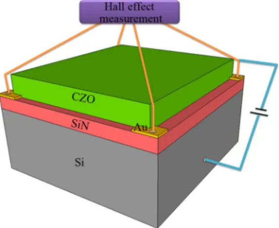
FIG. 3. The capacitor structure of the ZnxCo1-xO (CZO) device. CZO is
de-posited at the top of the whole structure to gain better x-ray signals. Four wires are connected to Au electrodes to enable the Hall effect measurements. A circuit connecting Si substrate and one of the Au electrodes is used to apply voltage upon the device. The illustration shows the case of negative applied voltage (injecting carriers), but the sign of the applied voltage can be switched to positive (extracting carriers) by reversing the sign at the power source.
schematically illustrates the details of the setup and acces-sories inside and outside the x-ray analytical chamber, re-spectively. The x-ray incident angle is 30◦with respect to the electromagnet as well as the normal direction of the sample, yet the incident angle can be adjusted by rotating the sample holder, which determines the x-ray probing direction.
B. Device design
The ZnxCo1-xO films (∼150 nm) were prepared at room
temperature by a multilayer doping technique with Co con-centration of about 5%, at Dept. Physics, National Sun Yat-sen University. Examination of the as-deposited films by x-ray, transmission electron microscopy, and x-ray absorption spectrum indicated no detectable precipitation of Co clusters or Co oxides. The electrical transport of samples, patterned with van der Pauw geometry,34 was tested using a standard four-point measurement technique independently from the E-X measurement to ensure the sample quality. The ZnxCo1-xO
device was prepared into a capacitor structure as shown in Fig.3, where SiN (75 nm) serves as the dielectric material and ZnxCo1-xO and Si serve as the top and bottom electrodes,
respectively. With such geometry the ZnxCo1-xO is fully
ex-posed to the x-ray for the purpose of acquiring clear sig-nals. We have tested other device structures with materials buried underneath several capping layers, and signals with fair good quality were accessed, as well. This means that the de-vice structure does not necessarily have to follow the princi-ple of the ZnxCo1-xO/SiN/Si case proposed here. Empirically,
we suggest a total thickness of the capping layers less than 80 nm, considering the penetration depth of the TFY.
The insulating SiN adjacent to the ZnxCo1-xO can
accu-mulate injected carriers at the ZnxCo1-xO/SiN interface upon
applied voltages. Four Au electrodes were patterned at the corners of the ZnxCo1-xO/SiN interface using e-gun
evapora-tion and photo-lithography. They were individually connected to four Pt wires to enable the Hall coefficient measurements
TABLE I. Voltage-dependent carrier concentrations for intrinsic and photo-induced cases measured by the E-X setup.
Applied bias
Intrinsic carrier concentration (number/cm3) Carrier concentration at Co L3-edge (number/cm3) −10 V 9.047×10¹⁹ 9.096×10¹⁹ 0 V 9.031×10¹⁹ 9.552×10¹⁹ +10 V 9.069×10¹⁹ 9.120×10¹⁹
with the magnetic field provided by the electromagnet. At this situation the ZnxCo1-xO/SiN/Si device needs to be set in
an out-of-plane (with respect to the magnetic field direction) mode as Fig.2shows. By measuring the Hall coefficient we can estimate the intrinsic (without x-ray shining) and photo-induced carrier concentration of the ZnxCo1-xO, and
compar-ing the two we can acquire the real quantity of the carriers participating in the mediation of the spin-polarization process. To assure the accuracy of the transport data all the connecting wires are of equal length to exclude the possible variations in sheet resistance, carrier concentration and electron mobil-ity. TableIlists the voltage-dependent carrier concentrations of the ZnxCo1-xO at room temperature, for both intrinsic and
photo-induced (photon energy set at Co L3-edge) cases. It can
be seen that though the photo-induced carrier concentration is larger than the intrinsic carrier concentration, they are in a close proximity in the order of magnitude. This is because that comparing to the x-ray spot size (∼0.1 mm (vertical) × ∼0.7 mm (horizontal)), the sample size (8 mm × 8 mm) is much larger, thus only causing a minor increase in photo-induced carrier concentration. For the ZnxCo1-xO/SiN/Si
de-vice, one of the Au electrodes is shared by another circuit with the other end connected to the Si substrate (Fig.3). By apply-ing positive/negative voltages through this circuit, charge car-riers can be injected-into/extracted-from the ZnxCo1-xO. This
allows us to monitor the band-filling effect with associated magnetization change from XAS/XMCD spectra.
C. Contact circuits on the sample holder
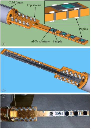
A sample holder made of oxygen-free copper is used in this study. The schematic illustration of the sample holder is presented in Fig.4(a). The holder is designed to be wide at top but narrow at bottom to allow the reduction of the electro-magnet gap, for the purpose of having a larger electro-magnetic field when the measurement is turned to an in-plane (with respect to the magnetic field direction) mode. Twenty Pt pins are set along the holder edges with equal spacing, and these pins tap through the holder as illustrated in the inset of Fig.4(a). The ZnxCo1-xO/SiN/Si device is placed on an Al2O3 substrate to
be insulated from the Cu holder, but it is connected to the pins with Pt wires for electrical polarization. On the back side of the holder, the pins are wound by enameled wires (Fig.4(b)), with the other ends fixed by 20 metallic screws located at the top of the holder. These 20 metallic screws are independently connected to 20 cables going outside the x-ray chamber to be electrically controlled by a remote Hall mea-surement system (Fig. 2). For electrical control experiment, only four channels (cables) at maximum can be operated at
123904-4 Huanget al. Rev. Sci. Instrum. 84, 123904 (2013)
FIG. 4. (a) Illustration of the sample holder particularly designed for the
E-X setup. Inset figure shows the details about the design specifically around
the sample and Al2O3substrate. (b) Back side of the holder, with the tapped
pins wound by enameled wires. (c) The real configurations of the employed circuits on the ZnxCo1-xO/SiN/Si device and the sample holder.
one time, so the Hall coefficient and carrier-injection (extrac-tion) measurements need to be carried out separately. Torr seal is used in the gray areas shown in Figs.4(a)and4(b)to en-sure that the given current is directed to the wanted path from source meter towards the device end without following into the Cu holder. A real picture showing the configurations of the employed circuits on the ZnxCo1-xO/SiN/Si device and the
sample holder is presented in Fig.4(c).
III. TEST CASE: XAS/XMCD SPECTRA OF ZnxCo1-xO UNDER APPLIED VOLTAGES
The capability of the E-X setup was tested by the ZnxCo1-xO with the device structure described above. This
material belongs to the Zn1-x(TM)xO (TM as transition
met-als) family,35–39 which has recently attracted much attention as a potential dilute magnetic semiconductor (DMS), be-cause it persists ferromagnetism (FM) above room temper-ature (RT). This makes it a more competitive candidate than the III-VI DMS systems. The classical mechanism explain-ing the RT-FM of the Zn1-x(TM)xO is the
bound-magnetic-polaron (BMP) model proposed by Coey,40 with a picture that the FM exchange is mediated by overlapped magnetic
polarons to enable a long range FM ordering. However, the BMP radius estimated by Coey is only about 0.76 nm, which is too small to enable a long range FM exchange if taking into account the very localized oxygen vacancies and magnetic dopant (typically below 5%) within a large sample volume. A modified-BMP model concerning the carrier-mediated FM ordering is proposed by Chou et al.,41where the carriers were found to hop via a variable-range hopping (VRH) mechanism to enable the FM exchange in addition to the BMP mecha-nism. This finding implies that when injecting carriers into the ZnxCo1-xO, the spin-polarized states of the dopant (Co)
and the host (ZnO) are expected to be modified and be accom-panied by complex electronic interactions between the two. This should be reflected by the XAS/XMCD spectra if tuning the x-ray resonance to the absorption edges of Co and O un-der applied voltages. In the following we present a serious of XAS/XMCD data to validate the hypothesis.
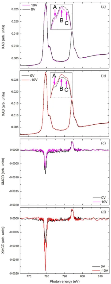
Figures 5(a)and 5(b)show the positive- and negative-voltage dependent Co L2/L3XAS, respectively at room
tem-perature. These two edges correspond to the 2p1/2/2p3/2→ 3d
photo-excited processes. For positive-voltage case, carriers are injected into the sample filling the unoccupied states of Co 3d orbital. This can be validated by the decreased XAS signal from zero to ten volts particularly at the L3-edge shown in
Fig. 5(a), because the XAS intensity is proportional to the number of unoccupied state. The feature of the decreased XAS takes place at A, B, C of the L3-edge as highlighted
in the inset of Fig. 5(a), which are associated with the changes of different electronic states. On the contrary, Fig.5(b)shows that the XAS intensity increases upon carrier extraction (negative-voltage), due to electrons withdrawn from the 3d orbital. The sensitive response of Co with respect to the applied voltage suggests that there likely exists a shal-low level in the vicinity of the Fermi level. Figures5(c)and
5(d)present the Co L2/L3XMCD corresponding to Figs.5(a)
and5(b), respectively. We observe an opposite dependency in XMCD as opposed to the XAS. This means that filling the electrons into Co tends to reduce the difference between the spin-up and spin-down DOS (a weaker spin-polarized state), but withdrawing the electrons does the opposite (a stronger spin-polarized state). We only see minor changes in O K-edge XAS and XMCD at room temperature (data not provided). This suggests marginal influence on the host upon injected carriers at room temperature, indicating very limited available states of O in the vicinity of the Fermi level hybridized with Co. A simple band structure based on the XAS/XMCD results and relevant Refs.42–45is illustrated in Fig.6, where we find that applying positive (negative) voltage is in a similar manner to lifting (lowering) the Fermi-level (EF). By lifting and lowering the EFwe are able to verify the band structure of the materials of interest. More importantly, we demonstrate the first case of electrically controlled spin-polarized electronic states of a spintronic material by probing the voltage-dependent XAS/XMCD. The Co XAS results unambiguously confirm the band-filling effects speculated by many relevant studies,9–11,25 and the associated XMCD results even offer more information about the spin-polarized states of a spintronic device while being electrically polar-ized. Finally, we take O K-edge XAS (Fig.7(a)) and XMCD
FIG. 5. (a) Positive- and (b) negative-voltage dependent Co L2/L3 XAS at
room temperature collected by the E-X setup. Decreased and increased XAS signals can be clearly obtained at A, B, and C at L3-edge shown in the insets
of (a) and (b), respectively. (c) and (d) are the positive- and negative-voltage dependent Co L2/L3XMCD, respectively.
FIG. 6. The simple band structure of the ZnxCo1-xO at room
tempera-ture. The band structure is illustrated based on the XAS/XMCD results and Refs.42–45.
(Fig.7(b)) at 20 K as an example to demonstrate the capabil-ity of the E-X setup at low temperature. In Fig.7(a), the XAS increases upon a voltage increase from zero to ten volts. The O XAS increase takes place at the post-edge which corre-sponds to the O 2p-Zn 4d orbital hybridization. Conversely, the O XMCD decreases upon voltage increase, as shown in Fig. 7(b). Obviously, at low temperature the host becomes more voltage-dependent. This could be attributed to less
FIG. 7. O K-edge (a) XAS and (b) XMCD collected at 20 K. In (a), pre-and post-edge features are divided into different orbital hybridizations (O 2p-Zn 4s, O 2p-2p-Zn 4p, and O 2p-2p-Zn 4d) by dashed lines. XMCD spectra are presented by dots instead of lines for the purpose of clarity, due to strong oscillation of the lineshape.
123904-6 Huanget al. Rev. Sci. Instrum. 84, 123904 (2013)
influence from the thermally excited carriers in the FM medi-ation process. Though more efforts are needed to unravel the underlying physics behind the scene, we have successfully demonstrated the reliable data acquired by the setup at various conditions, namely, XAS/XMCD spectra collected with temperature-, field-, and voltage-dependencies.
IV. SUMMARY
By combining a remote electrical control system and conventional soft x-ray absorption spectroscopy, a close-cycle helium cryostat and an electromagnet, we have devel-oped an synchrotron-based setup allowing the collection of XAS/XMCD spectra with in situ voltage-control and Hall measurements, at low temperatures (∼20 K) and moderate fields (1 tesla). We have demonstrated the capability of the setup by showing Co and O XAS/XMCD spectra of the ZnxCo1-xO under applied voltages. Taking advantage of
the setup we have shown the first case that in situ visual-ized the interplays between electronic and magnetic degrees of freedom while the system underwent magneto-electric re-sponses. This helps identify the roles of all physical vari-ables affecting the magneto-electric effects, which can fun-damentally improve the spintronic technology. Research top-ics related to (i) electrical control electronic structures and (ii) element-specific study of magneto-electric responses will be greatly benefited by the use of the setup.
ACKNOWLEDGMENTS
The author would like to thank Mr. Fan-Hsiu Chang for the XMCD data collection at NSRRC beamline 11A, and the fruitful discussions given by Dr. Horng-Ji Lin. Helps from Chen-Wei Yang, Wei-Chi Sung, Chih-Wen Tseng, Cheng-Jui Li, Hung-I Wang, and Hsuan-Chi Huang, on the trans-port measurements are greatly appreciated by the authors, as well. This work is supported by the National Science Council of Taiwan, under Grant No. NSC 101–2112-M-009 008-MY3.
1D. Grundler,Phys. Rev. Lett.84, 6074 (2000).
2A. W. Cummings, R. Akis, D. K. Ferry, J. Jacob, T. Matsuyama, U. Merkt,
and G. Meier,J. Appl. Phys.104, 066106 (2008).
3J. Jacob, G. Meier, S. Peters, T. Matsuyama, U. Merkt, A. W. Cummings,
R. Akis, and D. K. Ferry,J. Appl. Phys.105, 093714 (2009).
4R. Acharyya, H. Y. T. Nguyen, W. P. Pratt, Jr., and J. Bass,IEEE Trans.
Magn.46, 1454 (2010).
5T. Marukame, T. Ishikawa, T. Taira, K. Matsuda, T. Uemura, and M.
Yamamoto,Phys. Rev. B81, 134432 (2010).
6Y. Sakuraba, M. Hattori, M. Oogane, Y. Ando, H. Kato, A. Sakuma, T.
Miyazaki, and H. Kubota,Appl. Phys. Lett.88, 192508 (2006).
7M. Endo, S. Kanai, S. Ikeda, F. Matsukura, and H. Ohno,Appl. Phys. Lett.
96, 212503 (2010).
8H. Ohno, D. Chiba, F. Matsukura, T. Omiya, E. Abe, T. Dietl, Y. Ohno, and
K. Ohtani,Nature (London)408, 944 (2000).
9D. Chiba, M. Sawicki, Y. Nishitani, Y. Nakatani, F. Matsukura, and H.
Ohno,Nature (London)455, 515 (2008).
10T. Maruyama, Y. Shiota, T. Nozaki, K. Ohta, N. Toda, M. Mizuguchi, A. A.
Tulapurkar, T. Shinjo, M. Shiraishi, S. Mizukami, Y. Ando, and Y. Suzuki, Nat. Nanotech.4, 158 (2009).
11Y. Shiota, T. Maruyama, T. Nozaki, T. Shinjo, M. Shiraishi, and Y. Suzuki,
Appl. Phys. Express2, 063001 (2009).
12J. D. Burton and E. Y. Tsymbal,Phys. Rev. B80, 174406 (2009). 13C. A. F. Vaz, J. Hoffman, Y. Segal, J. W. Reiner, R. D. Grober, Z. Zhang,
C. H. Ahn, and F. J. Walker,Phys. Rev. Lett.104, 127202 (2010).
14P. Borisov, A. Hochstrat, X. Chen, W. Kleemann, and C. Binek,Phys. Rev.
Lett.94, 117203 (2005).
15V. Laukhin, V. Skumryev, X. Martí, D. Hrabovsky, F. Sánchez, M. V. G.
Cuenca, C. Ferrater, M. Varela, U. Lüders, J. F. Bobo, and J. Fontcuberta, Phys. Rev. Lett.97, 227201 (2006).
16Y. H. Chu, L. W. Martin, M. B. Holcomb, M. Gajek, S. J. Han, Q. He, N.
Balke, C. H. Yang, D. Lee, W. Hu, Q. Zhan, P. L. Yang, A. F. Rodríguez, A. Scholl, S. X. Wang, and R. Ramesh,Nature Mater.7, 478 (2008).
17M. Y. Zhuravlev, S. Maekawa, and E. Y. Tsymbal,Phys. Rev. B81, 104419
(2010).
18E. Y. Tsymbal and H. Kohlstedt,Science313, 181 (2006).
19M. Gajek, M. Bibes, S. Fusil, K. Bouzehouane, J. Fontcuberta, A.
Barthélémy, and A. Fert,Nature Mater.6, 296 (2007).
20J. P. Velev, C. G. Duan, J. D. Burton, A. Smogunov, M. K. Niranjan, E.
Tosatti, S. S. Jaswal, and E. Y. Tsymbal,Nano Lett.9, 427 (2009).
21V. Garcia, M. Bibes, L. Bocher, S. Valencia, F. Kronast, A. Crassous, X.
Moya, S. E. Vedrenne, A. Gloter, D. Imhoff, C. Deranlot, N. D. Mathur, S. Fusil, K. Bouzehouane, and A. Barthélémy,Science327, 1106 (2010).
22M. Weisheit, S. Fähler, A. Marty, Y. Souche, C. Poinsignon, and D. Givord,
Science315, 349 (2007).
23C. G. Duan, J. P. Velev, R. F. Sabirianov, W. N. Mei, S. S. Jaswal, and
E. Y. Tsymbal,Appl. Phys. Lett.92, 122905 (2008).
24T. Nozaki, Y. Shiota, M. Shiraishi, T. Shinjo, and Y. Suzuki,Appl. Phys.
Lett.96, 022506 (2010).
25K. Kyuno, J. G. Ha, R. Yamamoto, and S. Asano,J. Phys. Soc. Jpn.65,
1334 (1996).
26K. Nakamura, R. Shimabukuro, Y. Fujiwara, T. Akiyama, and T. Ito,Phys.
Rev. Lett.102, 187201 (2009).
27M. Tsujikawa and T. Oda,Phys. Rev. Lett.102, 247203 (2009).
28R. Shimabukuro, K. Nakamura, T. Akiyama, and T. Ito,Physica E42, 1014
(2010).
29M. K. Niranjan, C. G. Duan, S. S. Jaswal, and E. Y. Tsymbal,Appl. Phys.
Lett.96, 222504 (2010).
30J. A. Nielsen and D. McMorrow, Elements of Modern X-ray Physics,
2nd ed. (Wiley, 2011).
31G. Schütz, W. Wagner, W. Wilhelm, P. Kienle, R. Zeller, R. Frahm, and G.
Materlik,Phys. Rev. Lett.58, 737 (1987).
32C. T. Chen,Nucl. Instrum. Methods256, 595 (1987). 33C. T. Chen and F. Sette,Rev. Sci. Instrum.60, 1616 (1989). 34L. J. V. D. Pauw, Philips Res. Rep. 13, 1 (1958).
35K. Ueda, H. Tabata, and T. Kawai,Appl. Phys. Lett.79, 988 (2001) 36M. Venkatesan, C. B. Fitzgerald, J. G. Lunney, and J. M. D. Coey,Phys.
Rev. Lett.93, 177206 (2004).
37S. J. Pearton, C. R. Abernathy, M. E. Overberg, G. T. Thaler, D. P. Norton,
N. Theodoropoulou, A. F. Hebard, Y. D. Park, F. Ren, J. Kim, and L. A. Boatner,J. Appl. Phys.93, 1 (2003).
38A. D. Trolio, R. Larciprete, S. Turchini, and N. Zema,Appl. Phys. Lett.97,
052505 (2010).
39H. Gu, Y. Jiang, Y. Xu, and M. Yan,Appl. Phys. Lett.98, 012502 (2011). 40J. M. D. Coey, M. Venkatesan, and C. B. Fitzgerald,Nature Mater.4, 173
(2005).
41H. Chou, C. P. Lin, J. C. A. Huang, and H. S. Hsu,Phys. Rev. B77, 245210
(2008).
42J. I. Hong, J. Chol, S. S. Jang, J. Gu, Y. Chang, G. Wortman, R. L. Snyder,
and Z. L. Wang,Nano Lett.12, 576 (2012).
43M. Xu, H. Zhao, K. Ostrikov, M. Y. Duan, and L. X. Xu,J. Appl. Phys.
105, 043708 (2009).
44P. Sharma, A. Gupta, K. V. Rao, F. J. Owens, R. Sharma, R. Ahuja, J. M.
O. Guillen, B. Johansson, and G. A. Gehring,Nature Mater.2. 673 (2003).