Electrical properties of GaSe doped with Er
Yu-Kuei Hsu, Chen-Shiung Chang, and Wen-Chang Huang
Citation: Journal of Applied Physics 96, 1563 (2004); doi: 10.1063/1.1760238 View online: http://dx.doi.org/10.1063/1.1760238
View Table of Contents: http://scitation.aip.org/content/aip/journal/jap/96/3?ver=pdfcov Published by the AIP Publishing
Articles you may be interested in
Electrical and optical properties of p-type InGaN
Appl. Phys. Lett. 95, 261904 (2009); 10.1063/1.3279149
Optical and electrical properties of (1-101) GaN grown on a 7° off-axis (001)Si substrate Appl. Phys. Lett. 84, 4717 (2004); 10.1063/1.1758300
Electrical and optical properties of n- and p-InSe doped with Sn and As J. Appl. Phys. 93, 2301 (2003); 10.1063/1.1539558
Photoluminescence and free carrier interactions in erbium-doped GaAs J. Appl. Phys. 83, 4918 (1998); 10.1063/1.367293
Temperature dependence of galvanomagnetic properties for Gd doped and undoped p -type GaSe J. Appl. Phys. 83, 2030 (1998); 10.1063/1.366934
Electrical properties of GaSe doped with Er
Yu-Kuei Hsu and Chen-Shiung Changa)Institute of Electro-Optical Engineering, National Chiao Tung University, Hsinchu, Taiwan, Republic of China
Wen-Chang Huang
Department of Electronic Engineering, Kun Shan University of Technology, 949 Da Wan Road, Yung-Kang City, Tainan Hsien 710, Taiwan, Republic of China
共Received 29 December 2003; accepted 20 April 2004兲
Measurements of the Hall effect and Er-related luminescence were made on Er-doped GaSe. Deep-level transient spectroscopy共DLTS兲 was also performed. Hall measurements show that hole concentrations of 0.2%, 0.5%, and 1% Er-doped GaSe samples are 1.5⫻1017– 6⫻1017cm⫺3 at
room temperature, and that the mobility of these holes is in the range 22–34 cm2/V s. The temperature dependence of the hole concentration is explained using the two-acceptor model, in which one acceptor level is at around 65 meV above the valence band and the other one is at⬃158 meV. The DLTS measurements yield similar results. Furthermore, the shallow acceptor impurities contribute free hole carriers and act as radiative centers; the deep acceptor impurities are nonradiative centers, which are responsible for the quenching behavior of Er-related luminescence. The temperature dependence of the hole mobility can be understood as the combined scatterings of homopolar optical phonons and ionized impurities. © 2004 American Institute of Physics. 关DOI: 10.1063/1.1760238兴
I. INTRODUCTION
Gallium selenide共GaSe兲 exhibits large optical nonlinear-ity and is transparent to a wide range of wavelengths, whose properties make it highly promising for use in nonlinear optics.1 Moreover, GaSe is a native p-type semiconductor that belongs to the III-VI layered semiconductor family. It has a relatively large band gap energy of⬃2.0 eV, so impu-rity doping in GaSe has attracted much interest because of its potential applications to photoelectric devices that operate in the visible region.2Many researchers have reported the elec-trical and optical characteristics of GaSe doped with ele-ments in groups I, II, IV, and VII.3–7Hole concentrations of the order of 1015– 1016cm⫺3at room temperature have been
obtained by doping with Cd, Zn, Cu, and Ag.
The doping of semiconductors with rare earth共RE兲 ele-ments has also attracted significant attention. RE eleele-ments have partially filled 4 f shells, which are well screened by the outer closed orbitals of 5s2 and 5 p6. The intracenter transi-tions of 4 f electrons in various host materials give rise to sharp, atomlike, and emission spectra that are independent of temperature. Recently, the erbium ion, when incorporated into a semiconductor such as Si共Ref. 8兲 or GaN 共Ref. 9兲, has been shown to exhibit an intra-4 f transition at a wavelength of 1.54m, whose transition is important as a source of light in optical communication technology. Only a few research groups have investigated the erbium-doped GaSe crystal 共Er:GaSe兲. Lee et al.10
and Tagiev et al.11reported the opti-cal absorption and luminescence excitation spectra of the Er:GaSe crystal, respectively. The recombination
mecha-nisms of radiative centers in Er:GaSe crystal have already been obtained from measurements of photoluminescence 共PL兲.12 One important 2.064 eV emission band has been
found, and attributed to the transition between the conduc-tion band and the acceptor level at around 64 meV above the valence band. However, the electrical behavior of Er impu-rities as dopants in GaSe has not yet been investigated. This study concentrates on the Hall effect, the deep-level transient spectra 共DLTS兲, and free carrier related luminescence mea-surements of the Er:GaSe crystal. The activation energies of acceptor impurity levels are determined from the temperature dependence of the hole concentrations, DLTS, and measure-ments of Er-related luminescence. Moreover, the role of Er as a doping agent in GaSe is discussed. The scattering-dependent hole mobility in Er:GaSe at various temperatures is also analyzed.
II. EXPERIMENTAL PROCEDURE
The p-type Er:GaSe crystals used in this study were ob-tained by the Bridgmann method. Er with a purity of 99.95% was added, at 0.2, 0.5–1 at. %, to a stoichiometric melt of GaSe. Raw materials were enclosed in a well-cleaned quartz tube at 10⫺6Torr. Growth proceeded with a thermal gradient of 30 °C/cm and a growth rate of 2 cm/day. After growth, square samples with faces perpendicular to the c axis were prepared using a razor blade; their typical dimensions were 4⫻4⫻0.3 mm3.
The Hall coefficients were made using a four-point di-rect current Van der Pauw configuration at temperatures be-tween 80 and 300 K to obtain the effects of temperature on the concentration and mobility of carriers. The current was made to flow in the surface planes and a magnetic field 共⬃0.5 T兲 was applied perpendicular to these planes. The
a兲Author to whom correspondence should be addressed; Electronic mail:
1563
0021-8979/2004/96(3)/1563/5/$22.00 © 2004 American Institute of Physics [This article is copyrighted as indicated in the article. Reuse of AIP content is subject to the terms at: http://scitation.aip.org/termsconditions. Downloaded to ] IP:
ohmic contacts were soldered using high-purity indium and then all samples were heated to 600 K for 10 min at 10⫺6 Torr to improve the ohmicity of the contact.
The DLTS measurements were made on the Schottky barriers diode, which was formed by thermally evaporating Au onto a c surface plane.13 The pattern of the Schottky contact was a circle with a diameter of ⬇1 mm. The ohmic contact was formed on the same side by soldering high-purity indium. The Au/ p-GaSe Schottky diodes exhibited good rectification characteristics when forward biased. Each diode had an effective barrier height of 0.68 eV and forward characteristics with an ideality factor of n⫽1.79 at room temperature. This high ideality factor may be partially re-lated to the defects, caused by the preparing of the surface of the semiconductor. DLTS measurements were made at a bias of⫺1 V, pulsed periodically to 0 V to fill the traps. Transient capacitance signals were obtained using a test ac signal at 1 KHz with an amplitude of 100 mV at temperatures from 130 to 380 K. The error in the measured temperature was esti-mated to be under 1 K when the measurement was made.
Samples were cooled in a variable-temperature cryostat to make PL measurements. The samples were excited using a 488 nm line output from an argon laser at an intensity of ⬇10 W/cm2. Luminescence was collected and dispersed with
an HR 1000 Jobin-Yvon monochromator. An InGaAs detec-tor was used under cooling condition to measure the PL spectra.
III. RESULTS AND DISCUSSION
The hole concentration was determined from the Hall measurements by assuming a unit Hall factor.14Table I lists the typical resistivity, hole mobility, and hole concentration of three different Er:GaSe samples at room temperature. The values are compared with those of the undoped GaSe, which was grown under the same conditions. The estimated hole
concentration increased from ⬃1.5⫻1017 to ⬃6
⫻1017cm⫺3 in samples as the concentration of dopants
in-creased from 0.2 to 1 at. %; these values are one order of magnitude higher than those obtained with other dopants, as reported in GaSe.15Figure 1 plots the temperature-dependent hole concentration of three different Er:GaSe samples. Throughout the range of temperatures, the hole concentration in Er:GaSe samples increases with temperature. The tem-perature dependence of the carrier concentration can be in-terpreted by assuming that the semiconductor contains two acceptor levels, with ionization energies of Ea1 and Ea2, respectively. The following cubic equation for hole
concen-tration can be easily obtained by applying the neutrality con-dition under the nondegenerate assumption:16
p⫽ Na1 1⫹p Nvexp
冉
Ea1 kBT冊
⫹ Na2 1⫹p Nvexp冉
Ea2 kBT冊
, 共1兲where p represents the hole concentration, T is the absolute temperature, Na1 and Na2 are the doping concentrations of the acceptor impurities, kBis the Boltzmann constant, and is the degeneracy factor, which is taken to be 2 in this cal-culation. In Eq.共1兲, the density of states, Nv, and the
effec-tive mass mv* of the valence band are Nv⫽4.83
⫻1015T3/2(m v
*/m0)3/2 and mv*⫽(mh*⬜
2
mh*储)1/3, respectively, where m0, mh*⬜, and mh*储 are the free electron mass, the effective hole mass perpendicular to the共100兲 plane, and that parallel to the 共100兲 plane, respectively. Here, the effective hole masses mh*⬜⫽0.8m0 and mh*储⫽0.2m0, such that mv*
⫽0.5m0, are used in Eq.共1兲. The best fitting curves for the
concentrations of holes in the three different samples are quite close to the experimental results and are represented by the solid lines in Fig. 1. Table II lists values of Na1, Na2, Ea1, and Ea2 obtained from various samples. The deep and shallow acceptor energy levels are located at around 158 ⫾3 and 65⫾3 meV above the top of the valance band. The concentration increased with increasing erbium
concentra-TABLE I. The results of Hall effect measurement.
Initial Er concentration 共at. %兲 Hole concentration 共cm⫺3兲 共cmMobility2/V s兲 Resistivity 共⍀ cm兲 Undoped GaSe 1.058⫻1015 56.76 104 0.2% GaSe:Er 1.529⫻1017 34.073 1.199 0.5% GaSe:Er 2.084⫻1017 23.358 1.283 1.0% GaSe:Er 4.132⫻1017 22.44 0.784
FIG. 1. Hole concentrations as a function of reciprocal temperature in Er-:GaSe samples. The solid lines show the calculated hole concentrations from Eq.共1兲.
TABLE II. The parameters of fitting results from temperature dependence of Hall effect measurement.
Initial Er concentration 共at. %兲 Na1 共cm⫺3兲 共cmNa2⫺3兲 共meV兲Ea1 共meV兲Ea2 0.2% GaSe:Er 3.116⫻1015 5.549⫻1017 67.76 156.94 0.5% GaSe:Er 1.791⫻1016 1.291⫻1018 67.13 158 1.0% GaSe:Er 8.504⫻1016 4.506⫻1018 63.26 160.75
1564 J. Appl. Phys., Vol. 96, No. 3, 1 August 2004 Hsu, Chang, and Huang
tion in all Er:GaSe samples, at all levels of impurities. A comparison of the impurity level at an ionization energy of 65 meV obtained from Hall measurements with that obtained by PL measurement12 revealed that this acceptor state was not only a radiative center but also electrically active.
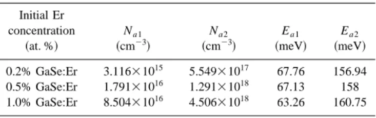
DLTS spectra were measured to obtain more information about the impurity level in Er:GaSe. Figure 2 displays the DLTS spectra from a 0.2% Er:GaSe sample. The applied pulse bias did not exceed the dc bias throughout the experi-ments, so only the impurity levels of majority carrier 共hole兲 traps were determined. Two peaks A and B were obtained at temperatures of about 240 and 370 K. The thermal emission rate eP was related to the activation energy of the trap level, Et, and the hole capture cross sectionP by the well-known equation17
eP⫽PvPNvexp共⫺Et/kBTM兲, 共2兲 wherevP is the average thermal velocity of holes and TM is the peak temperature of the DLTS signal. vP is assumed to vary as T1/2, and Nv as T3/2. The activation at a given trap level can be determined from the slope of ln(eP/TM
2
) vs 1/TM. Figures 3共a兲 and 3共b兲 present the Arrhenius plots that correspond to peaks A and B, respectively. The solid lines represent least-square fits and the activation energies of both acceptors are 65 meV and 158 meV. Moreover, the energies 65 meV and 158 meV are quite close to the activation ener-gies of the acceptor levels obtained by measuring the con-centration of holes. The trap level, corresponding to peak B detected by DLTS, at around 158 meV was not obtained by PL measurement in Ref. 12, suggesting that the trap state acceptor acts as a nonradiative center.
As measurements of the electric characteristics of Er-:GaSe, measurements of Er-related luminescence due to car-rier transitions yield more information about the level of im-purities. The 4 f -shell luminescence is involved in transferring energy from the semiconductor host to the Er 4 f core via Er-related defects, so luminescence associated with 4 f -shell transition can be observed. Figure 4 shows the PL
spectra of Er-related intra-4 f -shell luminescence from a 0.5% Er:GaSe sample at 35 K and at room temperature共300 K兲. The peak wavelength at around 1.54 m is associated with a transition from two spin-orbit interacting related manifolds (4I13/2→4I15/2). Apart from the peak at a
wave-length of 1.54 m, various additional peaks appeared at shorter wavelengths 共⬃1.52 m兲 as the temperature in-creased to 300 K. The additional peaks of Er correspond to the splitting patterns of the ground manifold (4I15/2) due to the surrounding crystal field caused by host atoms that sur-round Er. The main peaks共⬃1.54m兲 do not shift to longer wavelength over this wide range of temperatures because the intra-4 f transitions are shielded by the outer closed orbits. However, the integrated intensity is quenched by a factor of ⬇5 as the temperature is increased to 300 K. Figure 5 dis-plays the Arrhenius plot of the thermal quenching of the integrated intensity. At high temperature, the intensity is re-duced with an activation energy of about 162 meV. This
FIG. 2. DLTS spectrum of 0.2% Er:GaSe.
FIG. 3. Arrhenius plot of eP/TM
2 vs 1/T
Min peaks A and B.
value is almost the same as that of the deep acceptor level revealed by DLTS measurements. A similar behavior has also been reported to be exhibited by Er-doped GaAs and Yb-doped InP,18 whose excitation mechanisms have been com-prehensively studied. Hence, the corresponding quenching mechanism in this case is believed to involve the back trans-fer of energy. This mechanism is simply the reverse of Er3⫹ excitation; the excited Er3⫹ ion decays by capturing elec-trons and transfers its energy back to fill the deep acceptor state from the conduction band via a nonradiative process.
The doping of GaSe with erbium is now considered. Before the acceptor configuration can be explained with ref-erence to the impurity Er in GaSe, the reader should be aware that similar RE elements, such as gadolinium 共Gd兲,
doped in GaSe have been examined by electron paramag-netic resonance spectroscopy.19The doping process has been established to involve the replacement of one covalent-bound pair of gallium Ga24⫹atoms with one Gd3⫹atom, which acts
as an acceptor. The configuration of acceptors in GaSe has been speculated to be determined by the substitution of one Er3⫹ atom for one pair of Ga2⫹ atoms. In another possible model, Er3⫹ ions are interstitial at interlayer sites, corre-sponding to sites in between two layers of Se atoms, and bond with Se atoms in the octahedral configuration.15 This configuration will yield a Ga vacancy, which contributes to the character of the acceptor. Therefore, two acceptor levels are probably associated with Er atoms that are involved in the substitutional and interstitial processes in GaSe.
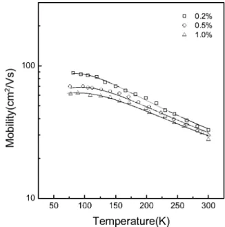
Figure 6 plots the temperature dependence of the hole mobility in Er:GaSe samples. The Hall mobility in Er:GaSe samples decreases as the temperature increases in the range 80–300 K. The hole mobility was determined by considering the mechanisms of scattering from both homopolar optical phonon and ionized impurities.
共i兲 Scattering due to 16.7 meV Al
⬘
homopolar optical phonon can be described using the Fivaz-Schmid relaxation time20⫽ ប共ប兲
1/2
3
冑
g2共kBT兲3/2, 共3兲
where g is a coupling constant for intraband interactions be-tween three-dimensional carriers and the homopolar optical branch, and បis the energy of the optical phonon.
共ii兲 Scattering due to ionized impurities is accounted for in the relaxation time approximation according to the known Brooks-Herring formula,21 ion⫽ 27/2m1/2共4兲2共k BT兲3/2 3/2e4Z2N i
冋
ln共1⫹兲⫺  1⫹册
共4兲FIG. 4. Er-related luminescence around 1.54m in 0.5% Er:GaSe at 35 K and room temperature.
FIG. 5. Temperature dependence of the integrated intensity for 4I13/2
→4I15/2emission.
FIG. 6. Hole mobility as a function of temperature in Er:GaSe samples.
1566 J. Appl. Phys., Vol. 96, No. 3, 1 August 2004 Hsu, Chang, and Huang
where ⫽(24m/n)(kBT/eប)2; N
i and eZ represent the concentration of ionized impurity and the ionic charge of the impurity, respectively.
The solid lines in Fig. 6 represent the results of this calculation. The theoretical behavior is experimentally sup-ported at various doping concentrations in Er:GaSe samples over the whole range of temperatures. The hole-phonon cou-pling constant g2 was determined to be 0.235, 0.243, and 0.252 at 0.2%, 0.5%, and 1.0% Er:GaSe, respectively. At low temperatures, the Hall mobility is limited by ionized impu-rity scattering, while at higher temperatures, the mobility of hole carriers is probably limited by the short-range interac-tion with homopolar optical phonons, polarized normally to the layers. The mechanism by which neutral impurities are scattered has not yet been elucidated. The Erginsoy relax-ation time22 of neutral impurities indicates that the mobility of holes can be affected when it is in the order of 104 cm2/V s at 300 K, which greatly exceeds the values measured herein; therefore, the neutral scattering mechanism is negligible herein.
IV. CONCLUSIONS
The electrical characteristics and Er-related lumines-cence of Er:GaSe samples were studied using Hall, DLTS, and PL measurements. The temperature dependence of car-rier concentration reveals that erbium introduced two accep-tor levels with ionization energies of Ea⬃65 and 158 meV. The measurements of DLTS and of the temperature depen-dence of Er-related luminescence indicate that the moder-ately deep acceptor level of 158 meV is importantly involved in the thermal quenching mechanism, which is associated with the energy back transfer process. Additionally, these acceptor levels could be associated with the substitution of two Ga2⫹ atoms by one Er3⫹ atom or are related to a Ga vacancy via the interstratifying of an Er3⫹ ion at the inter-layer site. The temperature dependence of hole mobility was also analyzed by scattering from homopolar optical phonons and ionized impurities.
ACKNOWLEDGMENTS
The authors would like to thank Professor W. F. Hsieh and Professor W. K. Cheng of National Chiao Tung Univer-sity for technical assistance during the experiment. This work was supported by the National Science Council of the Republic of China, Taiwan, under Contract Nos. 89-E-FA06-AB and NSC91-2112-M-009-036.
1S. Haidar, Y. K. Hsu, C. S. Chang, S. C. Wang, and H. Ito, Opt. Eng. 41,
1932共2002兲.
2S. Shigetomi, T. Ikari, and H. Nakashima, J. Appl. Phys. 74, 4125共1993兲. 3S. Shigetomi and T. Ikari, Philos. Mag. Lett. 79, 575共1999兲.
4V. Capozzi, Phys. Rev. B 28, 4620共1983兲.
5S. Shigetomi, T. Ikari, and H. Nakashima, Phys. Status Solidi A 156, K21 共1996兲.
6G. Micocci, A. Serra, and A. Tepore, J. Appl. Phys. 82, 2365共1997兲. 7S. Shigetomi, T. Ikari, and H. Nakashima, Jpn. J. Appl. Phys., Part 1 38,
3506共1999兲.
8T. Ishiyama, S. Nawae, T. Komai, Y. Yamashita, Y. Kamiura, T. Hasegawa,
K. Inoue, and K. Okuno, J. Appl. Phys. 92, 3615共2002兲.
9
A. J. Steckl, J. C. Heikenfeld, D. S. Lee, M. J. Garter, C. C. Baker, Y. Q. Wang, and R. Jones, IEEE J. Sel. Top. Quantum Electron. 8, 749共2002兲.
10W. S. Lee, N. O. Kim, and B. I. Kim, J. Mater. Sci. Lett. 15, 1644共1996兲. 11
B. G. Tagiev, F. S. Aidaev, and T. M. Abbasova, Solid State Commun. 66, 233共1988兲.
12Y. K. Hsu, C. S. Chang, and W. F. Hsieh, Jpn. J. Appl. Phys., Part 1 42,
4222共2003兲.
13W. Monch, Appl. Phys. Lett. 72, 1899共1998兲.
14A. Segura, F. Pomer, A. Cantarero, W. Krause, and A. Chevy, Phys. Rev.
B 29, 5708共1984兲.
15J. F. Sanchez-Royo, D. Errandonea, A. Segura, L. Roa, and A. Chevy, J.
Appl. Phys. 83, 4750共1998兲.
16
S. Blakemore, Semiconductor Statistics共Pergamon, New York, 1962兲.
17D. L. Lang, J. Appl. Phys. 45, 3023共1974兲.
18A. Taguchi and K. Takahei, J. Appl. Phys. 79, 4330共1996兲. 19
S. S. Ishchenko and A. A. Klimov, Phys. Solid State 40, 55共1998兲.
20Ph. Schmid, Nuovo Cimento Soc. Ital. Fis., B 21, 258共1974兲.
21H. Brooks, Advances in Electronics, and Electron Physics 共Academic,
New York, 1955兲, Vol. 7, p. 85.
22C. Erginsoy, Phys. Rev. 79, 1013共1950兲.