High-performance polycrystalline silicon thin-
film transistors prepared via the laser
crystallization of the prepatterned channel layer on the bottom-gate structure
Chao-Lung Wang
⁎
, I-Che Lee, Chun-Yu Wu, Yu-Ting Cheng, Po-Yu Yang, Huang-Chung Cheng
Department of Electronics Engineering, National Chiao Tung University, Hsinchu, Taiwan Institute of Electronics, National Chiao Tung University, Hsinchu, Taiwan
a b s t r a c t
a r t i c l e i n f o
Available online 5 October 2012 Keywords:
Excimer laser crystallization (ELC) Polycrystalline silicon
Prepatterned
Thin-film transistors (TFTs)
High-performance polycrystalline silicon thin-film transistors (TFTs) using an excimer laser crystallization of the prepatterned channel layer on the bottom-gate (BG) structure were fabricated to exhibit afield-effect mobility as high as 339 cm2/V s and an on/off current ratio of 9.5×10⁷with respect to 102 cm2/V s and
1.5×10⁷for the conventional top-gate (TG) TFTs, respectively. Such a superior performance is attributed to
the cross-shaped grain boundary structure formed in the channel region owing to the two-dimensional location control of grain boundaries. Moreover, the prepatterned BG TFTs show better device-to-device uniformity than the conventional TG ones due to the manipulated grain boundaries. This technology is thus promising for the future applications of system-on-panel and three-dimension integrated circuits.
© 2012 Elsevier B.V. All rights reserved.
1. Introduction
Low temperature poly-silicon (LTPS) thinfilm transistors (TFTs) have been extensively studied for the active-matrix-liquid-crystal displays (AMLCDs), active-matrix organic light-emitting displays (AMOLEDs), and three-dimensional integrated circuits (3D-ICs) applications[1,2]. The polycrystalline-Si (poly-Si) thinfilm transis-tors fabricated with conventional excimer laser crystallization (ELC) exhibit higherfield-effect mobility, typically about 100 cm2/V s, as compared to that of amorphous-Si (a-Si) TFTs. Therefore, the integra-tion of the peripheral driver circuits and pixel elements on the same glass substrate can be realized[3]. In the early stage of the develop-ment of LTPS TFTs, bottom-gate (BG) TFTs have attracted consider-able attention because it could be compatible with the process steps of traditional a-Si TFTs. However, the BG TFTs show worse electrical characteristics than the top-gate (TG) TFTs. Thefield-effect mobility of BG TFTs is generally lower than the TG ones because of the smaller grain size and poor crystallinity due to the BG electrode acting as the heat sink during ELC[4]. Therefore, adopting of TG TFTs in AMLCDs and AMOLEDs has become more popular than the BG ones. Although the ELC TG TFTs can achieve high field-effect mobility, the grain boundary distribution of ELC poly-Si films is non-uniform and randomly distributed. Consequently, ELC TG TFTs have encountered poor device-to-device uniformity, especially as the device dimension is comparable to the grain size and limits its practical applications for
small-dimension TFTs in high resolution panels[5,6]. Thus, various technologies aimed at the grain boundary location control, such as the sequential lateral solidification (SLS)[7], grainfilters method[8], grains controlled by air gap structure[9], dual-beam with thick oxide portion [10], and grains controlled by local heating system[11,12]have been proposed. However, based on these methods, the positions of the grain boundary can only be controlled one-dimensionally or require complex fabrication processes to enable the two-dimensional (2-D) location control of the grain boundaries.
In this paper, an ELC of the prepatterned channel layer on the BG structure has been adopted to fabricate the poly-Si TFTs. The prepatterned BG TFTs exhibited not only a superior device performance but also a much better device-to-device uniformity than the conven-tional TG ones owing to location-controlled grain boundaries. 2. Experimental details
Fig. 1 shows the schematic diagram of the key fabrication
sequence of laser irradiation on the prepatterned active layer with the BG structure. First, in-situ phosphorus doped poly-Si layer with a thickness of 1000 Å was deposited on an oxidized silicon substrate with a low pressure chemical vapor deposition (LPCVD) system at 550 °C as the BG electrode after definition. Then, a 1000-Å-thick tetraethyl orthosilicate (TEOS) gate oxide and a 1000-Å-thick a-Si thin film were deposited using LPCVD, followed by a 500-Å-thick capping TEOS oxide to prevent the a-Si from the ablation during laser irradia-tion. Then, the capping oxide and a-Si thinfilm were sequentially etched as the active region by transformer-coupled plasma reactive ion etching. After standard RCA clean process, the laser crystallization was performed using a KrF excimer laser (λ=248 nm) in a vacuum ⁎ Corresponding author at: National Chiao Tung University, Lab. ED 309B, Engineering
Bldg. 4, No. 1001, Ta-Hsueh Road, Hsinchu 30010, Taiwan. Tel.: +886 3 5712121x54218; fax: +886 3 5738343.
E-mail address:[email protected](C.-L. Wang). 0040-6090/$– see front matter © 2012 Elsevier B.V. All rights reserved. http://dx.doi.org/10.1016/j.tsf.2012.09.048
Contents lists available atSciVerse ScienceDirect
Thin Solid Films
chamber pumped down to 7.5× 10⁻⁶Pa at room temperature. The KrF excimer laser had a beam spot size of 23 mm×1.8 mm and the pulse width of 30 ns. After laser irradiation and capping oxide removal, phos-phorus ion implantation with a dose of 5×1015cm−2and an acceleration voltage of 40 keV was carried out to form the source and drain (S/D) regions. Next, a TEOS passivation oxide layer was deposited and the implanted dopants were activated by thermal annealing at 600 °C for 9 h in a furnace with nitrogen ambient. Finally, contact hole opening and metallization were completed to fabricate the prepatterned BG TFTs. No further hydrogenation plasma step was conducted during the device fabrication process. For comparison, conventional ELC TG TFTs with an average grain size of about 350 nm were also fabricated as the reference samples. After the TFTs fabrication, a semiconductor parameter analyzer (4156C, Agilent Technologies) integrated with a probe station was utilized to measure the current–voltage characteristics. After remov-ing the cappremov-ing oxide with Secco etchremov-ing, surface micrograph of the crys-tallized poly-Si thinfilms was observed by a field-emission scanning electron microscopy (FE-SEM; Hitachi S-4700I; operating voltage: 15 kV). An atomic force microscopy (AFM; Digital Instrument D3100) operated in the tapping mode with silicon probe of 10 nm tip radius is utilized to analyze the surface structure of the prepatterned channel layer after removing the capping oxide and exposed gate oxide. The transmission electron microscopy (TEM; JEOL JEM-2000FX; operating
voltage: 200 kV) was also adopted to analyze the cross-sectional device structures and the grain structure of the poly-Sifilms.
3. Results and discussion
Fig. 2(a)–(c) shows the SEM images of the Secco-etched poly-Si
thinfilms with the BG structure after the excimer laser crystallization and capping oxide removal for the gate length of 1.0, 1.2, and 2.0μm, accordingly. The constant laser energy density of 320 mJ/cm2 and shot numbers of 20 are adopted. It can be observed that four grains are formed in the channel region via the super lateral growth (SLG) and the cross-shaped grain boundary is therefore produced as the gate length is shorter than 1.2μm. In contrast, for the case of the gate length of 2.0μm, the spontaneous nucleation is observed in the channel region owing to the supercooling of the complete-melting
Excimer Laser Irradiation Bottom-gate
electrode
a-Si active layer Capping oxide Gate oxide Oxidized Si substrate Oxidized Si substrate Oxidized Si substrate Capping oxide a-Si active layer
Gate oxide
Capping oxide
Poly-Si active layer Gate oxide
Cross-shaped grain boundary
Grain growth direction
Fig. 1. Schematic diagram of the key processes for the TFTs prepared via the laser crystallization of the prepatterned channel layer on the BG structure.
1.0 µm
channel
Source
Drain
(a)
(b)
2.0 µm channel
Source
Drain
(c)
15.0 kV × 45.0K
1 µm15.0 kV × 45.0K
1 µm15.0 kV × 40.0K
1 µmFig. 2. SEM images of excimer-laser-crystallized poly-Si thinfilms with BG structure after Secco etching, in which the channel length is (a) 1.0μm, (b) 1.2 μm, and (c) 2.0 μm, respectively.
silicon before the grain growths impinge in the middle of the channel region. Therefore, small grains are caused by the spontaneous nucle-ation in the area of the channel region. As a result, by adopting a mod-erate gate length, like 1.0 or 1.2μm, the cross-shaped grain boundary structures can be formed in the channel region.
The dependence of the silicon grain structures on applied laser shot number is also investigated.Fig. 3(a) and (b) shows the Secco-etched SEM images of the prepatterned channel layer with the BG structure after laser irradiation shot of 1 and 20 times, corresponding-ly, for the gate length of 1μm. The cross-shaped grain boundary structures are produced in the channel region for both cases. The result indicates that the 2-D location-controlled grain boundary can be achieved only by a single shot of the ELC. The multiple shots of the laser pulse cannot change the cross-shaped grain boundary struc-ture in the channel region. However, the high density of intragrain defects formed under a single laser shot can be significantly reduced by multiple laser irradiations. Therefore, the 20 shots of laser pulse are adopted in this work to improve the crystallinity of the grain and device performance.
Fig. 4displays the cross-sectional TEM image to analyze the
micro-structure of the prepatterned BG TFT. The TEM sample is prepared using focused-ion-beam technology. The beam voltage and beam cur-rent used during the potentially damaging steps of etching process are 30 kV and 100 pA, respectively. As shown inFig. 4, it is observed that a single grain boundary perpendicular to the channel direction via the SLG phenomenon of the laser irradiation[13]. The electron diffraction image indicates that the silicon grain exhibits [110]-orientated with relation to the normal direction of the paper and the high crystallinity within the silicon grain due to the clear dot pattern.
Fig. 5(a) and (b) displays the cross-sectional surface roughness
anal-ysis of AFM images of the prepatterned channel layer with the BG struc-ture before laser irradiation and after laser irradiation, respectively. The
white dashed line Y–Y′ indicates the direction of the cross-sectional anal-ysis, as shown in the insets of the AFM images. It can be clearly observed that the edge of the prepatterned channel layer becomes thinner than the center along the Y–Y′ direction after the laser irradiation. The result is attributed to the shrinkage of the prepatterned channel owing to sur-face tension effect during laser irradiation[9]. Since the heat capacity of the thinner melting Si is smaller than the thicker one after the laser irra-diation, the edge of the channel will store the heat for a shorter time than the center of the channel. As a result, the edge of the channel will induce the temperature gradient from the center of the channel toward the edge and solidify atfirst.
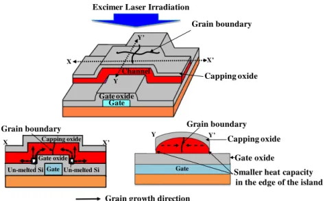
Fig. 6shows the schematic illustration of the mechanism of the
pro-posed crystallization method that causes 2-D location-controlled grain boundary. When the excimer laser irradiates on the prepatterned active layer, the laser energy density is controlled to melt the thin channel region completely. Since the laser energy density is almost uniform in the local region, the thick region of a-Sifilm near the edges of the BG structure will be only partially melted and the X–X′ directional temper-ature gradient is created. Therefore, the grain growths from the solid portions toward the melted region, resulting in one grain boundary per-pendicular to the channel direction in the middle of the channel region [11]. At the same time, the Y–Y′ directional temperature gradient is also produced on the prepatterned active layer, as mentioned above inFig. 5. Therefore, the lateral thermal gradient along the Y–Y′ axis occurs and the cooling rate of the edge region of the channel layer is faster than the central region. The Y–Y′ directional thermal gradient can lead to the grain growths from the edge of the channel toward the center so that a single grain boundary parallel to the channel direction is formed. Consequently, the grain boundary location is well-controlled two-dimensionally owing to the spatial thermal gradient distribution in the channel region.
Typical transfer characteristics of the prepatterned BG and conventional TG TFTs with W = L = 1μm are compared inFig. 7(a). Thefield-effect mobility and subthreshold swing are evaluated from the linear region at Vds= 0.1 V, and the on/off current ratio is defined at Vds= 1 V. It is clearly evident that the prepatterned BG TFTs exhibited obvious improvement in the device characteristics than
(a)
(b)
15.0 kV × 60.0K
500nm15.0 kV × 60.0K
500nmFig. 3. SEM images of excimer laser crystallized poly-Si thinfilms with BG structure after Secco etching, in which the channel length is 1μm, and the laser shot number is (a) 1 shot and (b) 20 shots, respectively.
100nm
Fig. 4. Cross-sectional TEM image and the diffraction pattern of excimer-laser-crystallized poly-Sifilms with BG structure.
the conventional TG ones. The prepatterned BG TFTs show a superior field-effect mobility of 339 cm2/V s, a low subthreshold swing of 0.354 V/dec, and a high on/off current ratio of 9.5 × 10⁷whereas the conventional ones show 102 cm2/V s, 0.722 V/dec and 1.5 × 10⁷ ,re-spectively. It is well known that the grain boundary acts a trapping
center and degrades the device electric characteristics. The better performance of the prepatterned BG TFT is attributed to the presence of only one perpendicular and one parallel grain boundary along the channel direction. To investigate the uniformities of the prepatterned BG and the conventional TG TFTs, twenty TFTs are measured for each.
Fig. 7(b) displays thefield-effect mobility distributions of these two
different TFTs for W = L = 1μm. The prepatterned BG TFTs exhibit a
µm
Y’
Y
Channel
Gate
oxide
Bottom-gate
electrode
(a)
Y’
Y
Channel
Gate
oxide
Bottom-gate
electrode
(b)
Distance (µm)
Distance (
µm)
Surface Roughness (nm)
Surface Roughness (nm)
Y’
Y
S
D
Y
Y’
S
D
Y’
nm
200 -200 0nm
0 0.50 1.00 1.50µm
0 0.50 1.00 1.50 200 -200 0Fig. 5. Cross-sectional surface roughness analysis of AFM images and the inset are the corresponding AFM images of the prepatterned channel layer with BG structure (a) before and (b) after laser irradiation.
Grain growth direction Excimer Laser Irradiation
Gate Channel Capping oxide Grain boundary Gate X’ X Y Y’ Grain boundary Grain boundary
Un-melted Si
Gate oxide
Smaller heat capacity in the edge of the island
X X’
Y Y’
Gate Un-melted Si
Gate oxide Gate oxide
Capping oxide
Capping oxide
Fig. 6. Illustration of the mechanism of the excimer laser crystallization of the prepatterned channel on the BG structure.
-10 -8 -6 -4 -2 0 2 4 6 8 10 10-12 10-11 10-10 10-9 10-8 10-7 10-6 10-5 10-4 W/L = 1 m/1 m Prepatterned BG TFT Conventional TG TFT
Gate Voltage V
gs(V)
Drain Current I
on(A)
0 50 100 150 200 250 300 350 400 450 500 550 600 650 700 750 800 850 900Field-Effect Mobility(cm
2/V-s)
(a)
Vds= 0.1V Vds= 1 V(b)
0 4 0 80 120 160 200 240 280 320 360 400 0 2 4 6 8 10 W/L = 1 m/1 mN
u
mber of
TFTs
Field-Effect Mobility(cm
2/V-s)
Prepatterned BG TFTs Conventional TG TFTsFig. 7. (a) Typical transfer characteristics and (b) measuredfield-effect mobility distributions of the prepatterned BG and conventional TG TFTs for W=L=1μm.
relatively smaller deviation in field-effect mobility (from 302 to 368 cm2/V s) than the conventional TG ones (71 to 213 cm2/V s). The superior device-to-device uniformity of the prepatterned BG TFTs as compared to the conventional TG ones can be ascribed to the much smaller deviation of the grain boundaries inside the channel region owing to the 2-D location-controlled grain boundary structure.
4. Conclusions
The 2-D grain boundary location-controlled method via excimer laser crystallization of the prepatterned channel layer on a BG structure has been proposed to accomplish the channel regions with the cross-shaped grain boundary structure. Consequently, the prepatterned BG TFTs could attain a higher field-effect mobility of 339 cm2/V s as compared with 102 cm2/V s for the conventional TG ones. Uniform device characteristics of the prepatterned BG TFTs were also demon-strated owing to the artificially controlled grain boundaries. It depicts that the proposed method is suitable for the system-on-panel and 3D-IC applications.
Acknowledgments
This work was supported by the National Science Council of the Re-public of China under the grant number NSC 99-2221-E-009-168-MY3,
and in part by the Nano Facility Center of National Chiao Tung University, and the National Nano Device Laboratories (NDL) for providing the process equipment.
References
[1] Y.I. Park, T.J. Ahn, S.K. Kim, J.Y. Park, J.S. Yoo, C.Y. Kim, C.D. Kim, in: SID Tech. Digest, 2003, p. 487.
[2] J.H. Park, P. Krishna, K.C. Saraswat, Hailin Peng, Appl. Phys. Lett. 91 (2006) 143107.
[3] M.H. Lee, S.L. Wu, M.J. Yang, K.J. Chen, G.L. Luo, L.S. Lee, M.J. Kao, IEEE Electron Device Lett. 31 (2010) 824.
[4] Y. Mishima, K. Yoshino, M. Takei, N. Sasaki, IEEE Trans. Electron Devices 48 (2001) 1087.
[5] P.C. Yang, P.S. Kuo, S.C. Lee, IEEE Trans. Electron Devices 55 (2008) 2129. [6] G.K. Giust, T.W. Sigmon, IEEE Electron Device Lett. 18 (1997) 296.
[7] M.A. Crowder, A.T. Voutsas, S.R. Droes, M. Moriguchi, Y. Mitani, IEEE Trans. Electron Devices 51 (2004) 560.
[8] R. Vikas, R. Ishihara, Y. Hiroshima, D. Abe, S. Inoue, T. Shimoda, W. Metsalaar, K. Beenakker, Jpn. J. Appl. Phys. 45 (2006) 4340.
[9] I.H. Song, S.H. Kang, W.J. Nam, M.K. Han, IEEE Electron Device Lett. 24 (2003) 580. [10] R. Ishihara, P.Ch.V.D. Wilt, B.D.V. Dijk, A. Burtsev, J.W. Metselaar, C.I.M. Beenakker,
Thin Solid Films 427 (2003) 77. [11] A. Asano, U.S. Patent 0290200 (2007).
[12] H. Jiroku, M. Miyasaka, H. Tokioka, and T. Ogawa, U.S. Patent 6602765 (2003). [13] C.C. Tsai, Y.J. Lee, J.L. Wang, K.F. Wang, I.C. Lee, C.C. Chen, H.C. Cheng, Solid State