novel way to fabricate poly-Si nanowire (NW)-silicon-oxide-nitride-oxide-silicon (SONOS) devices with various gate configu-rations. Three types of devices having various gate configurations, such as side gated, Ω-shaped gated ΩG, and gate-all-around (GAA), were successfully fabricated and characterized. The ex-perimental results show that, owing to the superior gate controlla-bility over NW channels, much improved transfer characteristics are achieved with the GAA devices, as compared with the other types of devices. Moreover, GAA devices also exhibit the best memory characteristics among all splits, including the fastest programming/erasing efficiency, largest memory window, and best endurance/retention characteristics, highlighting the potential of such scheme for future SONOS applications.
Index Terms—Field-effect transistor (FET), multiple gate
(MG), nanowire (NW), poly-Si, silicon-oxide-nitride-oxide-silicon (SONOS).
I. INTRODUCTION
S
ILICON-OXIDE-nitride-oxide-silicon (SONOS) multi-layer structure has been widely exploited in recent charge-trapping Flash applications in view of its potential to overcome the difficulties presenting in floating-gate Flash [1]–[3]. SONOS devices replace the poly-Si storage layer used in floating-gate devices with a nitride-trapping layer in which the charges are discretely stored in the traps of the nitride. Unlike the case of using floating poly-Si as the storage site, a single defect formed in the tunneling oxide would not cause any catastrophic failure, i.e., all stored charges would not leak out through the single defect; hence, improved data retention characteristics can be obtained. In addition, the SONOS struc-ture has a much-scaled height, as compared with the floating-gate structure, so the SONOS memory exhibits much stronger immunity against coupling interference. This is extremely im-portant in memory device scaling. In addition to main-stream high-density memory applications, currently, many studies have also been devoted to investigating the feasibility of applying SONOS structure to thin-film transistors (TFTs) for the purposeManuscript received April 28, 2010; revised November 13, 2010; accepted November 28, 2010. Date of publication January 24, 2011; date of current version February 24, 2011. This work was supported in part by the National Science Council under Contract NSC 96-2221-E-009-212-MY3. The review of this paper was arranged by Editor J. C. S. Woo.
The authors are with the Department of Electronics Engineering and Institute of Electronics, National Chiao Tung University, Hsinchu 300, Taiwan (e-mail: [email protected]).
Color versions of one or more of the figures in this paper are available online at http://ieeexplore.ieee.org.
Digital Object Identifier 10.1109/TED.2010.2098033
TFT-SONOS array could be vertically stacked to form 3-D configuration, allowing increased device density without ag-gressive scaling of device dimensions and also depressed power consumption.
It is imperative that SONOS-type memory devices possess low programming/erasing (P/E) operation voltage, high P/E speed, and excellent reliability. However, some challenging issues existing in poly-Si TFT-based thin-film memory devices, such as poor subthreshold swing (SS) and large leakage current, cause high P/E operation voltages and raise power dissipation concern. By utilizing nanowire (NW) channel in TFT structure, the SS and leakage current can be suppressed, owing to better gate controllability and much reduced cross-sectional area of leakage path [6]–[11]. Furthermore, since the NW channel is sensitive to its surface condition, a small amount of charge storage could change the threshold voltage VTH of memory device to obtain sufficient memory window [12], [13]. In this regard, the simulation results carried out by Fu et al. [14] have pointed out that, for a SONOS device with a cylindrical NW channel and gate-all-around (GAA) configuration, the electric field at the channel-to-gate dielectric interface can be three times higher than that of planar devices. Hence, P/E time or voltage could be dramatically decreased.
In this paper, we propose and demonstrate a simple and flexible way to fabricate novel poly-Si NW-SONOS devices without resorting to advanced lithographical tools such as e-beam writers. With a slight modification in fabrication pro-cedure of a previous scheme [10], three different types of gate configuration, namely, side gated (SG), Ω-shaped gated ΩG, and GAA, were implemented in the fabricated NW-SONOS devices. Moreover, the impacts of different gate configurations on memory characteristics such as P/E efficiency are compared and discussed. The information should be helpful to clarify how it affects the operation of NW devices and circuits.
II. DEVICESTRUCTURES ANDFABRICATION
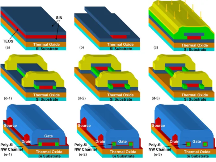
The key steps of device fabrication are illustrated in Fig. 1. First, three dielectric layers consisting of 50-nm bottom ni-tride, 40-nm tetraethyl orthosilicate (TEOS) oxide, and 30-nm dummy nitride were sequentially deposited by low-pressure chemical vapor deposition (LPCVD) on Si substrate capped with a thermal oxide [see Fig. 1(a)]. After the patterning of dummy nitride/TEOS oxide stack by anisotropic plasma etch-ing, further highly selective etching of the TEOS oxide with diluted HF was subsequently carried out to form the encroached
Fig. 1. Process flow for fabrication of the three types of poly-Si NW devices with various gate configurations.
Fig. 2. TEM images of the fabricated devices with (a) SG, (B)ΩG, and (c) GAA configuration.
rectangular-shaped cavities at the two sides of the patterns [see Fig. 1(b)]. Then, an undoped a-Si layer was deposited by LPCVD at 560 ◦C. By taking advantage of the excellent filling capability of LPCVD process, the cavities formed in the last step could be refilled by the deposited a-Si. An annealing step was then performed at 600 ◦C in N2, ambient for 24 h to transform the a-Si into a polycrystalline phase. Afterward, source/drain (S/D) implantation was performed, and then, the photoresist patterns covering the S/D regions were generated by a standard lithographic step. The main splits in this paper were accomplished by the following steps: For the SG devices, only an anisotropic dry etch was performed to remove poly-Si everywhere, except the portions covered by the photoresist or in the cavities that were shielded by the nitride hardmask [see Fig. 1(d-1)]. While forΩG split, additional wet-etch steps were
Fig. 3. Comparisons of the subthreshold characteristics of the fabricated devices.
performed to remove the nitride hardmask and then the dummy TEOS by hot H3PO4 and DHF, respectively [see Fig. 1(d-2)], whereas a portion of the bottom nitride was left intact to sustain the NW channels. Similar treatments were also ap-plied to the gate-all-around (GAA) devices, but the bottom nitride was further removed so that the NW channels are hanging between the S/D regions [see Fig. 1(d-3)]. Then, all splits were combined to receive the deposition of an ONO (4.5/8/10 nm) stack by LPCVD, capped with a 150-nm n+ poly-Si. The process temperature for ONO stack deposition is 700◦C
Fig. 4. (a) Programming and (b) erasing characteristics of the SG devices.
for SiO2and 780◦C for Si3N4. The dopant activation of the S/D implant was performed during the ONO LPCVD process. The poly-Si was sequentially patterned to serve as the gate electrode [see Fig. 1(e-1)–(e-3)]. A standard metallization scheme was then performed to complete the device fabrication. For the purpose of comparison, planar devices with poly-Si channel of 50 nm and same ONO condition were also fabricated.
Fig. 2 shows the cross-sectional transmission electron mi-croscopic (TEM) pictures of the three types of NW-SONOS devices. It should be noted that the cross-sectional dimensions of all NWs are comparable. Owing to the additional etch steps, the shapes of ΩG [see Fig. 2(b)] and GAA [see Fig. 2(c)] look more rounded than the SG split. The channel width of SG devices is about 20 nm for each NW channel, as shown in Fig. 2(a). ForΩG and GAA devices, the channel width is increased to 50 and 60 nm, respectively, due to the fact that extra NW edges are incorporated as the conductive channel.
III. BASICELECTRICALCHARACTERISTICS OF
POLY-Si NW-SONOS DEVICES
Fig. 3 shows typical transfer characteristics of the three types of NW-SONOS devices stated in Section II. In the figure, all measured devices have a channel length of 0.4 µm and equivalent gate-oxide thickness of around 20 nm. It can be noticed that the GAA device depicts the highest on-current and the smallest SS (∼150 mV/dec). The drain-induced-barrier-lowering phenomenon is also negligible for both GAA andΩG devices. These observations are expected since the GAA device has its NW channels surrounded by the gate, ensuring great gate controllability and suppressed effective defect density per-unit-gated area. While the SG device has only one of the NW surfaces under gate modulation, it results in the worst SS and the lowest on-current.
The aforementioned comparison unambiguously demon-strates the benefit of using GAA scheme to improve the device characteristics, although it needs extra etch steps to complete the structure, as mentioned in the previous section. Another issue associated with GAA devices is the failure of device characteristics as the channel is long. Specifically, we found that the drain current of GAA devices becomes too low to be measured as the channel length is longer than 2µm, implying that the NW channels have been broken. Such phenomenon, however, does not occur to the SG and ΩG splits. Consider-ing the difference in process steps and the resulted structure [see Fig. 1(d)], the failure of long-channel GAA devices is
Fig. 5. (a) Programming and (b) erasing characteristics of theΩG devices.
Fig. 6. (a) Programming and (b) erasing characteristics of the GAA devices.
Fig. 7. (Left) Simulated electric field distribution along the paths indicated by the arrows shown in (right) the 2-D simulation profiles of SG and GAA devices.
attributed to the collapse and breaking of the long NWs, which occurred after they were released and become suspended by removing the underlying nitride.
IV. P/E CHARACTERISTICS
Since the existence of potential barriers caused by the de-fects presenting in or near the grain boundaries of the poly-Si NW channel would hinder the acceleration of the electrons from source to drain, the channel-hot-electron-injection method is not appropriate for the programming operation of poly-Si NW-SONOS device. Therefore, in this paper, we employ Fowler–Nordheim (FN) tunneling mechanism [15] for all P/E operations of the fabricated NW devices. The threshold voltage
VTH of the devices is defined as VG@ID= W/L × 5 nA for
simplicity.
Fig. 4 depicts the P/E speed characteristics of SG NW-SONOS device with gate voltage VG ranging from 10 to 13 V. During the P/E operations, the source and the drain
Fig. 8. Simulated electric field along channel-width direction (y-direction) in the oxide at two locations, i.e.,X1 [(solid line) near channel surface] and X2 [(dot line) near gate], for an SG device.
were both grounded. The characteristics of planar TFT-SONOS counterpart with a gate bias of 15 V are also shown in Fig. 4(a). The experimental results clearly show that SG NW-SONOS device exhibits faster programming efficiency than planar coun-terpart. This could be partly attributed to the use of ultrathin NW channel that could significantly reduce the impact of the defects presenting in the channel and promote the programming current (see Fig. 3). Furthermore, due to the much more scaled channel width W = 20 nm), as compared with planar one
W = 5 µm), fringing-field enhancement at the channel edge
is more pronounced in the SG NW device, further benefiting the programming speed [16]. The erasing characteristics are shown in Fig. 4(b) in which the data of planar devices are not included since only negligible shift inVTH was detected even as aVG of −15 V was applied. As shown in the figure, the erasing characteristics show weak dependence on the applied
VGfor the SG devices. Such observation might be related to the
nonuniform trapping events happening in this type of devices and will be addressed later.
Figs. 5 and 6 show the P/E speed characteristics ofΩG and GAA NW-SONOS devices, respectively, with variousVG. As compared with Fig. 4, the P/E efficiency of ΩG and GAA devices is obviously improved. Moreover, the GAA device shows the fastest P/E speed among the three types of devices, indicating that the gate controllability has great impact on NW memory characteristics. The much improved P/E efficiency with GAA andΩG NW structures is believed to be related to the increase in curvature of the NW channels and the mulitple-gated (MG) configuration. Previous works on investigating the performance of metal–oxide–semiconductor field-effect tran-sistors and SONOS with NW channel [14], [17] have shown that the electric field in the gate oxide during operation is position- and curvature-dependent and favors the P/E operation for NW with a round-shaped NW. For example, during the programming operation, the electric field in the tunnel oxide is enhanced when the curvature of the channel surface increases [14]. Such argument is also applied to this paper. Fig. 7 de-picts the simulated electric-field distribution [18] based on the cross-sectional shapes of the fabricated SG and GAA devices extracted from the TEM analysis shown in Fig. 2(a) and (c). In the figure, for simplicity, a SiO2instead of ONO is used as the gate dielectric. The strength of the electric field in the oxide along the paths indicated by the arrows in the inset 2-D profiles
Fig. 9. Fresh, programmed, and erased subthreshold characteristics of the (a) SG, (b)ΩG, and (c) GAA devices.
is shown and compared for the two cases with a programming voltage of 10 V. It can be observed that the magnitude of the electric-field strength near the GAA-NW surface is 60% larger than that near the SG-NW surface due to the geometry of rounded structure. This is consistent with the analysis of a previous work [14] and reasonably in agreement with the faster P/E operations with the GAA configuration.
Another factor affecting device operation is the uniformity of electric-field strength during operation. This is related to
Fig. 10. Endurance characteristics of the (a) SG, (b)ΩG, and (c) GAA devices.
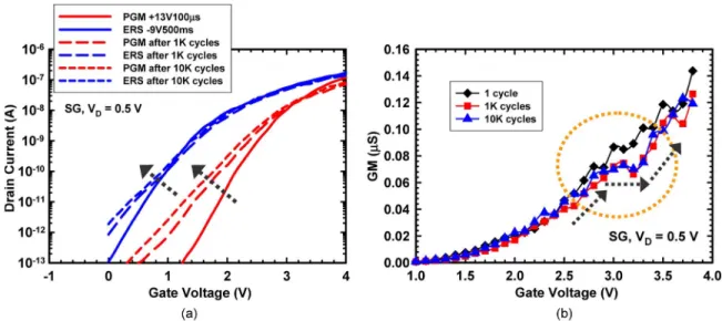
Fig. 11. (a) Subthreshold and (b) transconductance characteristics of an SG device after 1, 1K, and 10K P/E cycles of operation.
the curvature and, thus, the shape of the NW channel. Unlike the single-crystal Si NW, it is hard to form poly-Si NWs with their cross-sectional shape of symmetrical circle. The curvature, and thus the electric field strength, may vary from place to place at the NW surface. The nonuniform electric field may result in nonuniform charge trapping and detrapping during P/E operations [19], [20]. For the SG devices, the appearance of top and bottom corners would further worsen the situation.
The simulated magnitude of electric field strength along the channel-width direction (y-direction) for SG device at two positions in the gate oxide (X = X1 and X2) are shown in Fig. 8. In this case, a gate bias of−10 V is applied. Apparently, the electric field is position-dependent and has maximums at the locations where corner exists. Such electric field distribution may provoke nonuniform gate current density across the chan-nel surface [20] and therefore leads to inefficient P/E operation,
Fig. 12. Subthreshold characteristics of the (a)ΩG and (b) GAA devices after 1, 1K, and 10K P/E cycles of operation.
as shown in Fig. 4. It should be noted that, for simplicity, the simulation analysis shown in Figs. 7 and 8 are done with the assumption that the Si layer is monocrystalline. The existence of grain boundaries in the poly-Si channel may more or less affect practical device operation. However, we expect that the influence should not be significant because of the tiny volume of the poly-Si layer in which very limited amount of defects is contained [6], [11].
In contrast, for the GAA andΩG NW devices, the average curvature at the channel surface is increased, whereas its value is relatively uniform throughout the NW channel, as compared with the SG case. This results in improved P/E efficiency, particularly for the GAA samples. It should be noticed that the erasing speed of GAA device slows down when erasing time is sufficiently long (e.g., 0.1 ms with a gate bias of−12 V), as shown in Fig. 6(b). Moreover, the saturation (absolute) value of VTH shift is the smallest for a gate bias of−12 V among all bias splits. This is due to the preponderant electron injection from the n+ poly-Si gate, leading to a limited saturation level ofVTH. Higher work-function gate material such as p+poly-Si or TaN [21] would be helpful to relieve this problem.
The transfer curves of the three types of NW-SONOS devices at fresh state and specific P/E states are shown in Fig. 9. A memory window of 1.2 V can be achieved for the SG device with the programming gate voltage of VGP= 13 V and the erasing gate voltage ofVGE= −9 V, with duration of 100 µs and 500 ms, respectively [see Fig. 9(a)]. Since theΩG device depicts higher P/E speed, an increased memory window of 2 V can be achieved for theΩG device by applying VGP = 13 V
andVGE= −10 V with smaller duration of 10 µs and 100 ms,
respectively [see Fig. 9(b)]. For GAA device, memory win-dows of 2.3, 3, and 3.6 V can be obtained by applying
VGP = 11, 13, and 15 V with the same duration of 10 ΩG,
respectively [see Fig. 9(c)]. Finally, the duration of eras-ing operation can be reduced to 10 ms with VGE= −10 V for erasing the programmed GAA device back to the fresh
VTHlevel.
Fig. 13. Subthreshold swing as a function of P/E cycles for the three splits of NW devices.
The aforementioned results clearly indicate that the device with GAA configuration has the largest window and the fastest P/E speed among the three types of NW-SONOS devices. Higher average value and better uniformity of the channel-surface are believed to be the major reasons for the superiority of the GAA devices.
V. ENDURANCE ANDRETENTION
Fig. 10(a)–(c) show the endurance characteristics of the SG,ΩG, and GAA NW-SONOS devices, respectively. Again, the GAA device shows the best performance among the test samples in terms of the smallest closure in window size after 10K P/E++ stressing cycles. For the SG device, it is shown that the VTH values for both programmed and erased states slightly decrease after 10K P/E cycles. An opposite trend is observed for theΩG and GAA cases, i.e., the VTH values for both programmed and erased states increase with increasing
Fig. 14. Retention characteristics of the (a) SG, (b)ΩG, and (c) GAA devices at room temperature after 1 and 10K P/E cycles of operation.
cycles. Furthermore, the increasing rate becomes larger as cycle number is larger than 1K.
To gain more insight into these phenomena, the ID–VG characteristics of the SG device for various P/E cycles (1, 1K, and 10K) are shown and compared in Fig. 11(a). It is clearly shown that the SS becomes worse with increasing cycles. The primary reason for the SS degradation in the SG device could be ascribed to the nonuniform field strength during the previously mentioned P/E operations (see Fig. 8), which tends to result in nonuniform stored charges after cycles of operation. This is
Fig. 15. Retention characteristics of the GAA devices at 85◦C after 1 and 10K P/E cycles of operation.
evidenced by the transconductance (GM) versus theVGcurves extracted at erased state in Fig. 11(b). In the figure, we can clearly see a plateau region appearing inVGranging from 2.8 to 3.2 V (the arrows shown in the figure are used to elucidate the trend) after 1K and 10K cycles. This implies that theVTHalong the channel width direction is location dependent and supports the aforementioned inference.
Fig. 12(a) and (b) depict the ID–VG characteristics of the ΩG and GAA devices, respectively, during endurance tests. From the figures, the I–V curve after 1K cycles appears to be parallel to the fresh one, indicating that excessive electron storage is mainly responsible for the VTH shift. In the fig-ures, the I–V curves after 10K cycles show obvious increase in SS, representing one additional factor responsible for the
VTH increase in the programmed states. Such degradation is
mainly attributed to the generation of additional interface states at or near tunnel oxide/channel interface generated by the high-voltage stress during P/E operation. Owing to the much lower P/E voltages used, as compared with the planar devices (see Fig. 4), degradation of the oxide/channel interface is not significant until the cycle number reaches beyond 1K.
Fig. 13 shows and compares the SS versus P/E cycle numbers for the three types of NW-SONOS devices. As previously men-tioned, because of the severe nonuniformity in trapped charge distribution due to the large variation in surface curvature of the channel, the SG split exhibits obvious rising behavior in the beginning. Such circumstance is improved with theΩG and GAA devices, particularly for the latter that shows the least SS degradation. The SS value slightly increases in the first 10K P/E cycles, implying that theΩG and GAA devices may also suffer from the nonuniform charge injection effect, although far less significant as compared with the SG case. The increase in SS becomes more obvious after 10K cycles as additional interface traps appear.
The retention characteristics of the SG, ΩG, and GAA NW-SONOS devices with 1 P/E cycle and 10K P/E cycles at room temperature (25 ◦C) are shown in Fig. 14(a)–(c), respectively. Among the three types of NW devices, the GAA split depicts the largest memory window of about 1.7 and 1 V, respectively, after 10 years for the devices after single and 10K
shift with time than that of the device after 1 cycle of P/E operation. This is attributed to the detrapping of trapped holes in the tunneling oxide near the channel surface resulted during the P/E operations [23].
Fig. 15 shows the retention behaviors of GAA devices at 85◦C. TheVTHdecay rate in the programmed state is observed to be greater than that at room temperature, leading to a reduced memory window from the 10-year projection. This indicates that the emission of trapped electrons from the storage nitride is accelerated by the thermal-activated process [24]. Since the energy level of the hole traps is relatively deep in the nitride and the detrapping of holes contained in the tunneling oxide is mainly via tunneling mechanism [24], theVTHshift rate of the erased state should be insensitive to the temperature for both singly and 10K P/E-stressed devices, as shown in Figs. 14(c) and 15.
VI. CONCLUSION
In this paper, we have investigated the characteristics of poly-Si NW-SONOS with various gate configurations fabri-cated with an ingenious scheme. As compared with the planar counterpart, the NW devices can be operated with a much reduced P/E voltage, which is essential for the demand of green electronics. This is attributed to the enhanced gate con-trollability with MG configuration and the use of ultrathin NW structure with reduced impact of defects in the channel. Among the three types of NW devices, the GAA split exhibits the best performance in terms of the steepest subthreshold characteristics, the highest P/E efficiency, the largest memory window, and the best endurance and retention characteristics. This is attributed to the increase in the electric field strength at the NW/tunneling oxide interface owing to the large curvature and the reduced variation in the curvature value. Hence, the GAA device possesses the most prominent performance among the different types of devices characterized in this paper.
ACKNOWLEDGMENT
The authors would like to thank the National Nano Device Laboratories and the Nano Facility Center of National Chiao Tung University for the assistance in device fabrication.
REFERENCES
[1] M. H. White, D. A. Adams, and J. Bu, “On the go with SONOS,” IEEE
Circuits Devices Mag., vol. 16, no. 4, pp. 22–31, Jul. 2000.
[2] J. Bu and M. H. White, “Design considerations in scaled SONOS non-volatile memory devices,” Solid State Electron., vol. 45, no. 1, pp. 113– 120, Jan. 2001.
[6] M. Im, J.-W. Han, H. Lee, L.-E. Yu, S. Kim, S. C. Jeon, K. H. Kim, G. S. Lee, J. S. Oh, Y. C. Park, H. M. Lee, and Y.-K. Choi, “Multiple-gate CMOS thin-film transistor with polysilicon nanowire,” IEEE Electron
Device Lett., vol. 29, no. 1, pp. 102–105, Jan. 2008.
[7] N. Singh, A. Agarwal, L. K. Bera, T. Y. Liow, R. Yang, S. C. Rustagi, C. H. Tung, R. Kumar, G. Q. Lo, N. Balasubramanian, and D. L. Kwong, “High-performance fully depleted silicon nanowire (diameter≤ 5 nm) gate-all-around CMOS devices,” IEEE Electron Device Lett., vol. 27, no. 5, pp. 383–386, May 2006.
[8] H. C. Lin, M. H. Lee, C. J. Su, T. Y. Huang, C. C. Lee, and Y. S. Yang, “A simple and low-cost method to fabricate TFTs with poly-Si nanowire channel,” IEEE Electron Device Lett., vol. 26, no. 9, pp. 643–645, Sep. 2005.
[9] H. C. Lin, H. H. Hsu, C. J. Su, and T. Y. Huang, “A novel multiple-gate polycrystalline silicon nanowire transistor featuring an inverse-T gate,”
IEEE Electron Device Lett., vol. 29, no. 7, pp. 718–720, Jul. 2008.
[10] H. H. Hsu, T. W. Liu, L. Chan, C. D. Lin, T. Y. Huang, and H. C. Lin, “Fabrication and characterization of multiple-gated poly-Si nanowire thin-film transistors and impacts of multiple-gated structures on device fluctuations,” IEEE Trans. Electron Devices, vol. 55, no. 11, pp. 3063–3069, Nov. 2008.
[11] W. C. Chen, H. C. Lin, Y. C. Chang, C. D. Lin, and T. Y. Huang, “In-situ doped source/drain for performance enhancement of double-gated poly-Si nanowire transistors,” IEEE Trans. Electron Devices, vol. 57, no. 7, pp. 1608–1615, Jul. 2010.
[12] H. Yin, W. Xianyu, A. Tikhonovsky, and Y. S. Park, “Scalable 3-D fin-like poly-Si TFT and its nonvolatile memory application,” IEEE Trans.
Electron Devices, vol. 55, no. 2, pp. 578–584, Feb. 2008.
[13] J. Fu, Y. Jiang, N. Singh, C. X. Zhu, G. Q. Lo, and D. L. Kwong, “Polycrystalline Si nanowire SONOS nonvolatile memory cell fabricated on a gate-all-around (GAA) channel architecture,” IEEE Electron Device
Lett., vol. 30, no. 3, pp. 246–249, Mar. 2009.
[14] J. Fu, N. Singh, K. D. Buddharaju, S. H. G. Teo, C. Shen, Y. Jiang, C. Zhu, M. B. Yu, G. Q. Lo, N. Balasubramanian, D. L. Kwong, E. Gnani, and G. Baccarani, “Si-nanowire based gate-all-around nonvolatile SONOS memory cell,” IEEE Electron Device Lett., vol. 29, no. 5, pp. 518–521, May 2008.
[15] M. Lenzlinger and E. H. Snow, “Fowler-Nordheim tunneling into ther-mally grown SiO2,” J. Appl. Phys., vol. 40, no. 1, pp. 278–283, Jan. 1969.
[16] H. T. Lue, T. H. Hsu, Y. H. Hsiao, S. C. Lai, E.-K. Lai, S. P. Hong, M. T. Wu, F. H. Hsu, N. Z. Lien, C. P. Lu, S. Y. Wang, J. Y. Hsieh, L. W. Yang, T. Yang, K. C. Chen, K. Y. Hsieh, R. Liu, and C. Y. Lu, “Understanding STI edge fringing field effect on the scaling of charge-trapping (CT) NAND flash and modeling of incremental step pulse pro-gramming (ISPP),” in IEDM Tech. Dig., 2009, pp. 839–842.
[17] S. D. Suk, K. H. Yeo, K. H. Cho, M. Li, Y. Y. Yeoh, K. H. Hong, S. H. Kim, Y. H. Koh, S. G. Jung, W. J. Jang, D. W. Kim, D. G. Park, and B. I. Ryu, “Gate-all-around twin silicon nanowire SONOS memory,” in VLSI Symp. Tech. Dig., 2007, pp. 142–143.
[18] ISE TCAD Rel. 10.0 Manual, DESSIS, Zurich, Switzerland, 2004. [19] H. T. Lue, T. H. Hsu, S. Y. Wang, Y. H. Hsiao, E. K. Lai, L. W. Yang,
T. Yang, K. C. Chen, K. Y. Hsieh, R. Liu, and C. Y. Lu, “Study of local trapping and STI edge effects on charge-trapping NAND flash,” in IEDM
Tech. Dig., 2007, pp. 161–164.
[20] T. H. Hsu, H. T. Lue, Y. C. King, Y. H. Hsiao, S. C. Lai, K. Y. Hsieh, R. Liu, and C. Y. Lu, “Physical model of field enhancement and edge effects of FinFET charge-trapping NAND flash devices,” IEEE Trans.
Electron Devices, vol. 56, no. 6, pp. 1235–1242, Jun. 2009.
[21] C. H. Lee, K. I. Choi, M. K. Cho, Y. H. Song, K. C. Park, and K. Kim, “A novel SONOS structure of SiO2/SiN/A12O3with TaN metal gate for multi-giga bit flash memories,” in IEDM Tech. Dig., 2003, pp. 613–616. [22] Y. Wang and M. H. White, “An analytical retention model for SONOS
nonvolatile memory devices in the excess electron state,” Solid State
and the M.S. degree from National Chiao Tung University (NCTU), Hsinchu, Taiwan, in 2008. He is currently working toward the Ph.D. degree at the Institute of Electronics Engineering, NCTU.
His current research interests are the fabrica-tion and characterizafabrica-tion of Si nanowire field-effect transistors and memory devices.
Horng-Chih Lin (S’91–M’95–SM’01) was born in I-Lan, Taiwan, China, on August 1, 1967. He re-ceived the B.S. degree in physics from National Central University, Chung-Li, Taiwan, in 1989 and the Ph.D. degree in electronic engineering from National Chiao Tung University (NCTU), Hsinchu, Taiwan, in 1994.
From 1994 to 2004, he was with the National Nano Device Laboratories, where he has been en-gaged in the research projects of nanoscale device technology development. In 2004, he joined the faculty of NCTU, where he is currently a Professor with the Department of Electronics Engineering and the Institute of Electronics. He has authored or coauthored over 200 technical papers in international journals and confer-ences in the aforementioned areas. His current research interests include thin-film-transistor fabrication and characterization, reliability of complementary metal–oxide–semiconductor devices, and nanowire device technology.
Dr. Lin served on the program committee of the International Reliability Physics Symposium (2001 and 2002) and the International Conference on Solid State Devices and Materials (2005–2008).
Chun-Jung Su was born in Tainan, Taiwan, in 1979. He received the B.S. degree in materials science and engineering and the Ph.D. degree in electronic engineering from National Chiao Tung University, Hsinchu, Taiwan, in 2002 and 2008, respectively.
His research interests include the fabrication and characterization of poly-Si thin-film transistors and Si nanowire devices.
Tiao-Yuan Huang (S’78–M’78–SM’88–F’95) re-ceived his B.S.E.E. and M.S.E.E. degrees from National Cheng Kung University, Tainan, Taiwan, in 1971 and 1973, respectively. After serving two years in the Taiwanese navy as fulfillment of his conscription duty, he left for the U.S. in 1977 and received his Ph.D. degree from the University of New Mexico, Albuquerque, in 1981.
He worked in the U.S. Semiconductor Industry for 14 years, prior to his return to his native country, Taiwan. Since 1995, he has been a Professor with the Department of Electronics Engineering, National Chiao Tung University, Hsinchu, Taiwan.
Prof. Huang was elected as an IEEE Fellow in 1995. He was also the recipient of the Semiconductor International’s Technology Achievement Award for his invention and demonstration of the fully overlapped lightly doped drain metal–oxide–semiconducting transistors.
![Fig. 8. Simulated electric field along channel-width direction ( y-direction) in the oxide at two locations, i.e., X1 [(solid line) near channel surface] and X2 [(dot line) near gate], for an SG device.](https://thumb-ap.123doks.com/thumbv2/9libinfo/7645926.138820/4.891.480.807.107.911/simulated-electric-channel-direction-direction-locations-channel-surface.webp)