The Effect of Film Thickness on the Electrical Properties of LPCVD
Polysilicon Films
N. C. C. Lu
IBM Thomas J. Watson Research Center, Yorktown Heights, New York 10598
C.Y. Lu
The Institute of Electronics, National Chiao-Tung University, Hsin-Chu, T a i w a n , China and Department of Electrical and Computer Engineering, North Carolina State University, Raleigh, North Carolina 27650
M. K. Lee, C. C. Shih, and C. S. Wang
The Institute o f Electronics, National Chiao-Tung University, Hsin-Chu, T a i w a n , China
W. Reuter
IBM Thomas J. Watson Research Center, Yorktown Heights, New York 10598
T. T. Sheng
A T & T Bell Laboratories, Murray Hill, New Jersey 07974 A B S T R A C T
T h e e f f e c t of film t h i c k n e s s on t h e electrical p r o p e r t i e s of b o r o n - d o p e d L P C V D p o l y s i l i c o n films w i t h d o p i n g con- c e n t r a t i o n r a n g i n g f r o m 1 x 10¹⁷ to 1 x 10 TM c m -3 h a s b e e n c h a r a c t e r i z e d f r o m 1.2 ~ m d o w n to 0.1 ~m. T h e r e s i s t i v i t y in- c r e a s e s e x p o n e n t i a l l y as t h e film t h i c k n e s s d e c r e a s e s , r a t h e r t h a n r e m a i n i n g c o n s t a n t , a n d t h e rate of i n c r e a s e is a s t r o n g f u n c t i o n of d o p i n g c o n c e n t r a t i o n . A f t e r a q u a n t i t a t i v e s t u d y on t h e p h y s i c a l m e c h a n i s m s w h i c h c a n affect t h e re- sistivity as film t h i c k n e s s decreases, t h e carrier t r a p p i n g e f f e c t d u e to grain-size v a r i a t i o n at d i f f e r e n t film t h i c k n e s s e s is s h o w n to b e t h e d o m i n a n t factor. A t r a p p i n g m o d e l w i t h o u t a s s u m i n g t h e d e p l e t i o n a p p r o x i m a t i o n can e x p l a i n w e l l t h e e x p e r i m e n t a l d a t a a n d e n h a n c e s u n d e r s t a n d i n g of t h e r e s i s t i v i t y b e h a v i o r as t h e p o l y s i l i c o n film t h i c k n e s s de- creases. P o l y c r y s t a l l i n e - s i l i c o n (polysilicon) m a t e r i a l is c o m - p o s e d of a g g r e g a t e s of single crystal g r a i n s w i t h a g r a i n b o u n d a r y b e t w e e n a d j a c e n t grains. T h e g r a i n b o u n d a r y is a t r a n s i t i o n a l r e g i o n b e t w e e n d i f f e r e n t o r i e n t a t i o n s of n e i g h b o r i n g crystallites. P o l y s i l i c o n films h a v e b e e n w i d e l y u s e d in i n t e g r a t e d circuits s u c h as silicon gates, in- t e r c o n n e c t i o n s , p a s s i v a t i o n or i s o l a t i o n layers, d i f f u s i o n sources, resistors, m o n o l i t h i c d i s t r i b u t e d RC filters, di- odes, a c t i v e d e v i c e s , a n d r e d u n d a n c y p r o g r a m m i n g ele- m e n t s . Its i n c r e a s i n g r a n g e of a p p l i c a t i o n s e n s u r e s t h e i m p o r t a n c e of this m a t e r i a l in t h e c o m i n g era of V L S I . S i n c e t h e d e m a n d for b e t t e r p e r f o r m a n c e a n d h i g h e r p a c k i n g d e n s i t y of V L S I circuits r e q u i r e s t h e d e v i c e size to be s c a l e d n o t o n l y in t h e h o r i z o n t a l b u t also in t h e v e r t i c a l d i r e c t i o n , t h e t h i c k n e s s of p o l y s i l i c o n films u s e d in m o s t i n t e g r a t e d - c i r c u i t a p p l i c a t i o n s h a s b e e n s c a l e d f r o m s e v e r a l m i c r o m e t e r s (1, 2) d o w n to t e n t h of a mi- c r o m e t e r (3). I n a d d i t i o n , t h e film d e p o s i t i o n g e n e r a l l y has c h a n g e d f r o m a t m o s p h e r i c - p r e s s u r e c h e m i c a l v a p o r d e p o s i t i o n ( A P C V D ) (1, 2) to l o w - p r e s s u r e c h e m i c a l v a p o r d e p o s i t i o n ( L P C V D ) (4) for b e t t e r film q u a l i t y a n d h i g h e r t h r o u g h p u t . As a result, u n d e r s t a n d i n g of t h e t h i c k n e s s scaling e f f e c t on t h e electrical p r o p e r t i e s of L P C V D p o l y s i l i c o n films in t h e s u b m i c r o m e t e r r a n g e is i m p o r - t a n t for d e v i c e d e s i g n in V L S I circuits. K a m i n s (1) s t u d i e d t h e t h i c k n e s s d e p e n d e n c e of Hall m o b i l i t y a n d r e s i s t i v i t y in A P C V D p o l y s i l i c o n films, w h i c h h a d t h i c k n e s s r a n g i n g f r o m 3 to 24 ~ m a n d w e r e d o p e d b y d i f f u s i o n w i t h c o n c e n t r a t i o n s r a n g i n g f r o m 10 '8 to 1019 c m -3. R e s i s t i v i t y of t h e s e p o l y s i l i c o n films de- c r e a s e s w i t h i n c r e a s i n g film t h i c k n e s s . K a m i n s s h o w e d t h a t this d e c r e a s e in r e s i s t i v i t y is d u e m a i n l y to t h e in- c r e a s e of m o b i l i t y . B e c a u s e an A P C V D p o l y s i l i c o n film w i t h t h i c k n e s s l a r g e r t h a n s e v e r a l m i c r o m e t e r s is c o m - p o s e d of a f e w layers of grains s t a c k e d in t h e t h i c k n e s s di- rection, t h e m e a s u r e d m o b i l i t y is a c t u a l l y an a v e r a g e mo- bility o v e r t h e film t h i c k n e s s . T h e m o b i l i t y n e a r t h e t o p s u r f a c e is l a r g e r in a t h i c k e r film b e c a u s e t h e g r a i n size b e c o m e s larger. Mei et al. (5) s t u d i e d t h e resistivities of A P C V D p o l y s i l i c o n films w h i c h h a d t h i c k n e s s d o w n to 0.25 ~ m a n d w e r e d o p e d b y p h o s p h o r u s i o n i m p l a n t a t i o n w i t h a c o n c e n t r a t i o n of 1.2 x 10¹⁹ c m -3. T h e r e s i s t i v i t y also d e c r e a s e s w i t h i n c r e a s i n g film t h i c k n e s s . It was rea- s o n e d t h a t this r e s i s t i v i t y i n c r e a s e is d u e m a i n l y to d o p a n t s e g r e g a t i o n to t h e i n t e r f a c e b e t w e e n p o l y s i l i c o n film a n d its u n d e r l y i n g o x i d e layer. R e c e n t l y , C o l i n g e et al. (6) p r o p o s e d a t h e o r e t i c a l e q u a t i o n [Eq. [5] in (6)] for t h e m o b i l i t y in p o l y s i l i c o n films, w h i c h c o n s i d e r s t h e ef- f e c t of film t h i c k n e s s b y including--the p o l y s i l i c o n / o x i d e i n t e r f a c e s c a t t e r i n g m e c h a n i s m . T h e y u s e d 1.95 ~ m as t h e m e a n free p a t h of e l e c t r o n s in silicon, w h i c h i m p l i e s t h a t if a p o l y s i l i c o n film t h i c k n e s s is r e d u c e d to t h e r a n g e of 1.95 ~m, t h e effect d u e to collisions of e l e c t r o n s to t h e p o l y s i l i c o n / o x i d e i n t e r f a c e c a n b e c o m e a d o m i n a n t factor to c a u s e t h e r e s i s t i v i t y increase. T h e a b o v e r e v i e w s h o w s t h a t t h e e f f e c t Of film thick- ness on t h e e l e c t r i c a l p r o p e r t i e s of L P C V D p o l y s i l i c o n films at d i f f e r e n t d o p i n g c o n c e n t r a t i o n s has n o t b e e n fully u n d e r s t o o d a n d that, in fact, d i f f e r e n t v i e w p o i n t s ex- ist on t h e d o m i n a n t m e c h a n i s m for t h e r e s i s t i v i t y c h a n g e s as t h e film t h i c k n e s s decreases. I n t h i s work, t h e r e f o r e , w e first c h a r a c t e r i z e d t h e electrical p r o p e r t i e s o f b o r o n - d o p e d L P C V D p o l y s i l i c o n films w h i c h h a d t h i c k n e s s r a n g i n g f r o m 1.2 d o w n to 0.1 ~ m a n d d o p i n g c o n c e n t r a - t i o n r a n g i n g f r o m 1 • 10 '7 to 1 x 10¹⁹ c m -~. It will b e s h o w n t h a t as t h e film t h i c k n e s s decreases, t h e r e s i s t i v i t y i n c r e a s e s e x p o n e n t i a l l y , r a t h e r t h a n r e m a i n i n g c o n s t a n t as in c o n v e n t i o n a l r e s i s t o r materials, a n d t h e rate of in- c r e a s e is a s t r o n g f u n c t i o n of d o p i n g c o n c e n t r a t i o n . T h e r e are several p o s s i b l e p h y s i c a l m e c h a n i s m s to c a u s e this in- crease, s u c h as p o l y s i l i c o n / o x i d e i n t e r f a c e scattering, d o p a n t s e g r e g a t i o n to t h e g r a i n b o u n d a r i e s , d o p a n t l e a c h i n g or loss, d o p a n t s e g r e g a t i o n to t h e polysili- c o n / o x i d e interface, a n d c h a n g e s of t h e n u m b e r of carri- ers t r a p p e d into grain b o u n d a r i e s b e c a u s e of grain-size variations. A d e t a i l e d q u a n t i t a t i v e analysis will s h o w t h a t t h e d o m i n a n t m e c h a n i s m c a u s i n g t h e r e s i s t i v i t y i n c r e a s e is t h e carrier t r a p p i n g effect d u e to grain-size r e d u c t i o n .
Experimental Results
Sample preparation and m e a s u r e m e n t s . - - U n d o p e d p o l y s i l i c o n films 0.1-1.2 ~tm t h i c k w e r e d e p o s i t e d o n t o 0.80 ~ m t h i c k SiO2 layers t h e r m a l l y g r o w n on silicon wa- fers. T h e d e p o s i t i o n was d o n e in an L P C V D r e a c t o r at 620~C b y H2 a m b i e n t pyrolysis of sflane w i t h a d e p o s i t i o n rate of 80 A/min. T h e i m p l a n t e d b o r o n d o s e s w e r e se- l e c t e d to g i v e c a l c u l a t e d d o p i n g c o n c e n t r a t i o n s at t h r e e d i f f e r e n t levels: 1 x 10¹⁷, 2 • 10 '8, a n d 1 x 10 TM c m -3. T h e c a l c u l a t i o n s a s s u m e d a u n i f o r m d o p a n t profile a n d no d o p a n t loss. T h e i m p l a n t a t i o n e n e r g i e s w e r e s e l e c t e d to yield a m a x i m u m i m p l a n t a t i o n d o s e n e a r t h e c e n t e r of t h e p o l y s i l i c o n films. A f t e r t h e d e v i c e s w e r e p a t t e r n e d b y p l a s m a e t c h i n g , a 0.80 ~tm-thick C V D o x i d e layer w a s de- p o s i t e d at 430~ C o n t a c t w i n d o w s w e r e o p e n e d , a n d t h e wafers w e r e d i v i d e d into t w o groups. O n e g r o u p h a d t h e c o n t a c t w i n d o w s i m p l a n t e d h e a v i l y w i t h b o r o n to give p+ 897
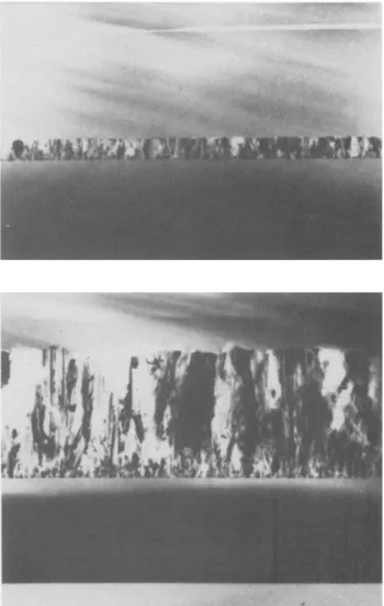
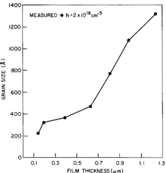
8 9 8 J. Electrochem. Soc.: S O L I D - S T A T E S C I E N C E A N D T E C H N O L O G Y A p r i l 1984 c o n t a c t s ; t h e o t h e r g r o u p d i d n o t h a v e t h i s i m p l a n t a t i o n . All t h e w a f e r s w e r e t h e n a n n e a l e d a t 900~ for 420 r a i n i n N2 to r e m o v e t h e i m p l a n t a t i o n d a m a g e a n d to e n s u r e u n i - f o r m d o p a n t d i s t r i b u t i o n . A 1 . 0 / ~ m - t h i c k a l u m i n u m l a y e r w a s d e p o s i t e d a n d d e f i n e d o v e r t h e c o n t a c t areas. T h e c o n t a c t s w e r e a l l o y e d at 450~ for 20 m i n i n N2. T h e de- v i c e s i n c l u d e d d i f f e r e n t s h a p e s o f r e s i s t o r s , v a n d e r P a u w s t r u c t u r e s (8), a n d c r o s s - b r i d g e s t r u c t u r e s (8). T h e t h i c k n e s s o f p o l y s i l i c o n film w a s m e a s u r e d b y a n a - s t e p profiler. T h e g r a i n s t r u c t u r e a n d g r a i n size w e r e s t u d i e d u s i n g t r a n s m i s s i o n e l e c t r o n m i c r o s c o p y (TEM) t e c h n i q u e s . F i g u r e 1 s h o w s t h e t y p i c a l c r o s s - s e c t i o n a l T E M m i c r o g r a p h s . I t w a s f o u n d t h a t all t h e g r a i n s t r u c - t u r e s o f u n d o p e d a n d d o p e d s a m p l e s w e r e c o n i c a l , a n d n o s i g n i f i c a n t r e c r y s t a l l i z a t i o n w a s o b s e r v e d , i n c o n t r a s t to t h e r e p o r t e d g r a i n g r o w t h i n p h o s p h o r u s - d o p e d s a m p l e s i n Ref. (9). F r o m t h i n to t h i c k p o l y s i l i c o n films, t h e sur- face r o u g h n e s s b e c o m e s w o r s e , a n d t h e g r a i n size a t t h e t o p o f t h e s u r f a c e , w h i c h c o r r e s p o n d s a p p r o x i m a t e l y to t h e d i s t a n c e b e t w e e n t h e h i l l o c k s (9), i n c r e a s e s . A q u a n t i - t a t i v e m e a s u r e m e n t of t h e grain, size w a s p e r f o r m e d u s i n g t o p - v i e w e d T E M m i c r o g r a p h s s h o w n i n Fig. 2. T w o m e t h - o d s w e r e u s e d , a n d t h e r e s u l t s a g r e e d well. O n e m e t h o d w a s to m e a s u r e t h e a r e a of a c e r t a i n r e g i o n a n d to c o u n t t h e n u m b e r o f g r a i n s w i t h i n t h a t area. T h e a v e r a g e g r a i n size L is c a l c u l a t e d f r o m t h e f o l l o w i n g e q u a t i o n L = ( a r e a / n u m b e r o f grains)~ [1] w h e r e m is t h e m i c r o g r a p h m a g n i f i c a t i o n factor. T h e o t h e r m e t h o d (10) w a s to d r a w a l i n e a n d to c o u n t t h e n u m b e r o f g r a i n s a c r o s s t h e line. T h e a v e r a g e g r a i n size is L --. (line l e n g t h / n u m b e r of g r a i n s ) / m [2] T h e m e a s u r e d g r a i n size d e c r e a s e s as t h e film t h i c k n e s s d e c r e a s e s (Fig. 3). B y u s i n g t h e s e c o n d a r y i o n m a s s s p e c t r o s c o p y ( S I M S ) t e c h n i q u e (11), d o p a n t p r o f i l e s w e r e p r o v e n u n i f o r m , a n d n o s i g n i f i c a n t d o p a n t loss w a s o b s e r v e d . T h e S I M S a n a l - y s i s w a s d o n e w i t h a 12 k e V 02 + b e a m r a s t e r s c a n n e d a n d g a t e d to a c c e p t 20% of t h e c e n t r a l p o r t i o n . C h a r g i n g p r o b - l e m s w e r e m i n i m i z e d b y u s i n g t h e e l e c t r o n flood g u n a n d i n t e g r a t i o n of t h e s e c o n d a r y i o n e n e r g y d i s t r i b u t i o n . We u s e d a 50 k e V b o r o n i m p l a n t a t i o n w i t h d o s e of 5 x 10¹⁴ c m -2 as a s t a n d a r d . T h e m e a s u r e d d o p i n g c o n c e n t r a - t i o n s w e r e w i t h i n 20% o f t h e p r o j e c t e d v a l u e s . F i g u r e 4 s h o w s t y p i c a l S I M S p r o f i l e s o f s a m p l e s w h i c h h a v e pro- j e c t e d d o p i n g l e v e l s o f 2 • 10 TM c m -3 ' a n d t h i c k n e s s o f ei- t h e r 0.2 or 1.0 ~ m . E l e c t r i c a l m e a s u r e m e n t s i n c l u d e d t h e I-V c h a r a c t e r i s - tics, r e s i s t i v i t y , a n d H a l l v o l t a g e s . R e s i s t i v i t y w a s a l w a y s m e a s u r e d o v e r t h e l i n e a r I-V r a n g e w i t h s m a l l a p p l i e d bias. S h e e t r e s i s t a n c e s for s o m e h i g h - v a l u e r e s i s t o r s w e r e d i f f i c u l t to o b t a i n f r o m t h e H a l l s e t u p a n d w e r e c a l c u l a - ted, t h e r e f o r e , f r o m m e a s u r e d r e s i s t a n c e a n d d e v i c e g e o m e t r y . Results.--The m e a s u r e d s h e e t r e s i s t a n c e vs. film t h i c k - n e s s at r o o m t e m p e r a t u r e is s h o w n i n Fig. 5a for a d o p i n g
Fig. 1. Cross-sectional TEM micrographs. A, top: t = 1950A, N = 1 • 1017 cm -3. B, bottom: t = 9 8 0 0 A , N = 2 x 10 '8 cm -~. t - film thickness, N = doping concentration.
c o n c e n t r a t i o n o f 1 • 1017 c m -~, a n d i n Fig. 5b for 2 x 10¹⁸ c m -3. T h e c o n t a c t s b e t w e e n a l u m i n u m a n d p o l y s i l i c o n i n s a m p l e s w i t h o u t p+ c o n t a c t d o p a n t s a r e o h m i c at s m a l l a p p l i e d v o l t a g e . I n c l u s i o n o f t h e p+ c o n t a c t d o p a n t s d o e s n o t s i g n i f i c a n t l y a f f e c t t h e s h e e t r e s i s t a n c e . F i g u r e 5a a n d 5b s h o w s t h a t w h e n t h e film t h i c k n e s s d e c r e a s e s , t h e s h e e t r e s i s t a n c e i n c r e a s e s e x p o n e n t i a l l y . T h e t h i c k n e s s d e p e n d a n c e o f t h e r e s i s t a n c e is c o n s i d e r a b l y l a r g e r a t a d o p i n g c o n c e n t r a t i o n o f 2 x 10 TM c m -3 t h a n a t 1 x 10 '7 c m -3. T h e r e s i s t i v i t y , w h i c h c a n b e c a l c u l a t e d b y m u l t i - p l y i n g t h e s h e e t r e s i s t a n c e b y t h e film t h i c k n e s s , is also
I-ig. 2. Top view TEM micrographs of the samples in Fig. 1
) unless CC License in place (see abstract).
ecsdl.org/site/terms_use
address. Redistribution subject to ECS terms of use (see
140.113.38.11
1400
LPCVD POLYSILICON FILMS
899
1200 1000J
,,, 800 N 09 Z ~< 600 ( . 9 400 M 200Vol. 131, No. 4
0 I I I I I I 0.1 0.3 0.5 0.7 0.9 I.I FILM THICKNESS (p.m)Fig. 3. Measured average grain size v s . film thickness
1.3 s h o w n in Fig. 5a a n d 5b as a f u n c t i o n of film t h i c k n e s s . A r a p i d i n c r e a s e of t h e resistivity w i t h d e c r e a s i n g film t h i c k n e s s occurs, e s p e c i a l l y at t h i c k n e s s less t h a n 0.8/~m. T h i s b e h a v i o r is d i f f e r e n t f r o m o h m i c r e s i s t o r s o f o t h e r materials, t h e r e s i s t i v i t y of w h i c h is g e n e r a l l y i n d e p e n - d e n t of t h i c k n e s s . T h e o r e t i c a l I n t e r p r e t a t i o n T w o t h e o r i e s h a v e b e e n p r o p o s e d to m o d e l t h e trans- p o r t p r o p e r t i e s of d o p e d - p o l y s i l i c o n films. T h e first is a d o p a n t - s e g r e g a t i o n m o d e l , w h e r e t h e g r a i n b o u n d a r y s e r v e s as a s i n k to cause p r e f e r e n t i a l s e g r e g a t i o n of z F- Z bJ Z 0 o co z 0 c3
,o,,
I
I I, ', ~ i : : ~ ' ,~;', ', ' , . . . . - -,o"
tpoly
0 2 F r o \ / | 1017 Jr I 1016 p o l y - Si i S i 0 2 t 0.8 0.4 0 F I L M T H I C K N E S S (/~m) Fig. 4. Measured dopant profiles vs. film thicknessd o p a n t a t o m s t h a t b e c o m e i n a c t i v e at t h e b o u n d a r y (12, 13). T h i s m o d e l , h o w e v e r , c a n n o t e x p l a i n t h e m o b i l i t y m i n i m u m at a critical d o p i n g c o n c e n t r a t i o n , t h e t e m p e r a - t u r e d e p e n d e n c e of t h e resistivity, a n d t h e h y p e r b o l i c - sine I-V b e h a v i o r of p o l y s i l i c o n resistors at h i g h electric field. T h e s e c o n d t h e o r y is a carrier t r a p p i n g m o d e l (1, 2, 7, 14-16), w h e r e t h e t r a p p i n g states i n s i d e t h e g r a i n b o u n d a r y , d u e to defects a n d i n c o m p l e t e a t o m i c b o n d - ings, can trap free carriers f r o m t h e i o n i z e d dopants. T h i s p r o c e s s n o t o n l y r e d u c e s t h e n u m b e r of free carriers, b u t also c r e a t e s a p o t e n t i a l barrier s u r r o u n d i n g t h e grain b o u n d a r y , w h i c h i m p e d e s t h e m o t i o n of carriers f r o m o n e crystallite to another. T h i s m o d e l b e t t e r e x p l a i n s t h e sharp c h a n g e s of r e s i s t i v i t y w i t h d o p i n g c o n c e n t r a t i o n , t h e m o b i l i t y m i n i m u m , t h e t e m p e r a t u r e d e p e n d e n c e of resistivity, a n d t h e h y p e r b o l i c - s i n e I-V b e h a v i o r at h i g h
~
10 I0 o z w ~ IO 9 U.l .,r I0 II 10 7 I I I I I I I N : I x l O 17cm "3\z~ WITH CONTACT: Z~(G/o), o(D-cm) WITHOUT CONTACT: &(,O,/u), 9 (D,-cm)
\
o 108 I I I I I I I i 0 4 0.1 0 3 0.5 0.7 0.9 I.I 1.3 FIEM THICKNESS (p.m) io 6 o M ) -F.-
> 1--I05 ~
Fig. 5. Measured sheet resistance and resistivity v s . film thickness
at room temperature. A, above: N = ] • 1017 cm -3. B, right: N = 2 • 10 TM cm ~. 108
io 7
LU o z oo 106 hi E LU LU "T" (/) 10 5 10 4~ \ \
o = I I I I 1 I - 103 N = 2 x l O 18cm -3WITH CONTACT: Z~(D,/o), o(D,-cm) WITHOUT CONTACT: & (,O,/u), 9 (~-cm)
102 I0 I
- - - ~ - _ _ ~ _ _
I0 oI
t i " ~ - , a
IO-I 0.7 0.9 I.I 1.3 I I I 0.1 0.5 0.5 A E o i v ).. I- > I-- u) IJJ n- FILM THICKNESS (/J.m)900 J. Electrochem. Soc.: S O L I D - S T A T E
electric field. Even if the dopants do segregate, the trapping m o d e l can still be applied, based on an active dopant concentration that can be obtained by sub- tracting the inactive dopant concentration from the actual doping concentration (15, 17).
For thin-film polysilicon resistors, several physical m e c h a n i s m s may cause the observed resistivity increase when film thickness decreases. The effect of these mech- anisms will be considered individually below.
Scatterings at horizontal grain boundaries and poly-
silicon/oxide interface.--TEM results on L P C V D films
show that the grain structures in all samples having dif- ferent film thicknesses are conical. In such conical struc- tures, grain boundaries rarely occur in t h e direction paral- lel to the polysilicon/oxide interface, in contrast t o the randomly stacked grain structures usually observed in APCVD polysilicon films. If the structure had m a n y stacked layers of such horizontal grain boundaries, the re- sistances of the samples with p+ contact dopants could not be the same as those without the contact dopants be- cause the grain boundary is a high resistance region. However, it is found that the resistances of samples with p+ contact dopants are approximately equal to those with- out p+ contact dopants. This demonstrates that, even though horizontal grain boundaries may exist occasion- ally, they do not seriously disturb the current flow, and the possibility of carriers colliding with the horizontal grain boundaries is low. Since the m e a n free path of carri- ers in the intrinsic silicon is approximately 200A, 1 w h i c h is m u c h smaller than the thinnest film thickness in our samples, the carriers should have had several collisions before scattering at the polysilicon/oxide interface. As a result, the scattering effects due to both polysilicon/oxide interface and horizontal grain-boundaries should not be the d o m i n a n t factor responsible for the resistivity in- crease (18) in L P C V D polysilicon films with thickness down to 0.1 ~m. Another piece of indirect evidence to support the conclusion is that w h e n the oxide layer above polysilicon film is removed, the m e a s u r e d resistance does not change too m u c h from the resistance of samples with the top oxide layer present, and the rate of resistivity increase as the films b e c o m e thinner is almost the same. In addition, that different rates of the resistivity increase at different doping concentrations is difficult to explain based on scattering effect.
Dopant segregation to grain boundaries.--Although the
a m o u n t of dopant segregation to grain boundaries can be a function of film thickness, Mandurah et al. (19) showed that no significant segregation effect occurs in boron- doped polysilicon films. In our boron-doped samples, the grain-boundary segregation should not be the d o m i n a n t factor for the resistivity increase.
Dopant leaching or loss.--After inplantation and before
annealing, the samples were coated with a thin layer of low t e m p e r a t u r e deposited oxide to protect their surfaces from furnace ambient and to prevent loss of dopants dur- ing the high t e m p e r a t u r e process. The SIMS results (Fig. 4) p r o v e d that the actual doping concentration in the polysilicon film is close to the projected value within 20% variation, and no significant loss was found even in the thinnest samples.
Segregation to polysilicon/oxide interface.--From the
SIMS results as shown in Fig. 4, no significant pileup of the dopants was found at the polysilicon/oxide interface in t h e s a m p l e s w i t h d o p i n g c o n c e n t r a t i o n u p to 2 x I0 ~8 c m -3. It s h o u l d b e n o t e d t h a t a n e l e c t r o n f l o o d g u n for c h a r g e c o m p e n s a t i o n w a s e m p l o y e d . W h i l e n o t s h o w n in Fig. 4, t h e silicon s i g n a l r e m a i n e d c o n s t a n t w h e n s p u t - t e r i n g t h r o u g h t h e S i / S i O 2 interface. It h a s b e e n s h o w n (20) t h a t at n o r m a l i n c i d e n c e 0 2 + b o m b a r d m e n t , silicon is c o m p l e t e l y o x i d i z e d to SiO2. A t a d o p i n g level o f 1 • 1019 c m -~, a s m a l l p i l e u p o f t h e d o p a n t s h a s b e e n o b s e r v e d ; h o w e v e r , its a m o u n t is n o t s o significant a s to affect t h e a b s o l u t e d o p i n g level in t h e film. T h i s effect c a n b e c o m e i m p o r t a n t at h i g h e r d o p i n g c o n c e n t r a t i o n .
T h e m e a n free p a t h k is Vth(m*~t/q), w h e r e vth is t h e r m a l veloc- ity of the carriers, vth = ( 3 k T / m * ) ~ a n d ~ is mobility. In intrinsic silicon, X ~ 2 3 7 A for holes a n d ~ 2 0 4 A for electrons at r o o m t e m - perature. In a d o p e d silicon crystallite, k is e v e n smaller. F o r ex-
2 O 3
a m p l e , k ~ 1 3 0 A at a d o p i n g concentration of a r o u n d i0 c m - .
S C I E N C E A N D T E C H N O L O G Y A p r i l 1984
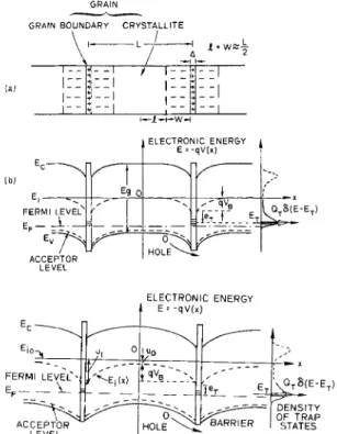
Carrier trapping.--Before a q u a n t i t a t i v e calculation of the carrier t r a p p i n g effect on the resistivity c h a n g e due to r e d u c t i o n of film thickness, general features of the carrier t r a p p i n g m o d e l are briefly r e v i e w e d here. Several a s s u m p t i o n s were m a d e in the p r e v i o u s t r a p p i n g m o d e l s (2, 15) to simplify the calculation. The polysilicon film is a s s u m e d to be c o m p o s e d of identical crystallites h a v i n g a grain size L, and the grain b o u n d a r y is a s s u m e d to contain Qv c m -~ of traps located at an en- ergy level of eT with respect to the intrinsic F e r m i level at the grain b o u n d a r y (Fig. 6). The traps are a s s u m e d to Re initially neutral and b e c o m e charged by t r a p p i n g car- hers. When d o p a n t s are a d d e d into polysilicon films, s o m e of the m o b i l e carriers a r o u n d t h e grain b o u n d a r y are t r a p p e d by the t r a p p i n g states in the grain boundary, resulting in a d e p l e t i o n region. U s i n g t h e s e assump- tions, an a b r u p t d e p l e t i o n a p p r o x i m a t i o n was used to calculate the e n e r g y band in the crystallites. F o r a g i v e n grain size, since the effective t r a p p i n g states in the grain b o u n d a r y are finite, t h e r e exist two possible conditions, d e p e n d i n g on the doping level. If the d o p i n g concentra- tion is high, t h e crystallite can only be partially d e p l e t e d and a neutral region r e m a i n s (Fig. 6b). If the d o p i n g level is d e c r e a s e d to a critical d o p i n g c o n c e n t r a t i o n N*, the crystallite is totally d e p l e t e d (Fig. 6c). Because the crystallite b e c o m e s totally depleted, the n u m b e r of free carriers r e m a i n i n g in the crystallite drastically de- creases, thus causing a sharp resistivity increase. As the doping level further decreases, the crystallites r e m a i n in the c o n d i t i o n of total depletion, and resistivity increases at a rather gradual rate. This explains w h y the resistivity vs. doping c o n c e n t r a t i o n c u r v e of polysilicon films has a sharp change in slope near the critical d o p i n g level N*. Similarly, at a g i v e n doping concentration, t h e r e exists a critical grain size L* b e l o w w h i c h the grains are totally depleted. F o r a grain size around the v a l u e of L*, as the grain goes f r o m partial to total depletion, t h e resistivity change due to grain size variation is drastic.
As m e n t i o n e d above, TEM results s h o w e d that w h e n polysilicon film t h i c k n e s s is reduced, the grain size de- creases. T h e effect of such grain-size c h a n g e on the re- sistivity of polysilicon films will be e x a m i n e d based on the carrier t r a p p i n g m o d e l below.
The p r e v i o u s t r a p p i n g m o d e l s (2, 14, 15) using the de- pletion a p p r o x i m a t i o n can clearly describe the t r a n s p o r t
(a> GRAIN GRAIN BOUNDARY I . . . . I IZZ - - I Ii- - - - I I CRYSTALLITE I : = --
I
E,-- _ !1 E : O FERM, I ACCEPTOR LEVEL ELECTRONIC ENERGY i s : -qV(x)" " ~e~ -q-V-e E OTS(E'ET)
FE R M/LE ~1-" "l ~ E : ( : ) - E F ~ ~ LEVEL ELECTRONIC ENERGY , E = -qV(x) ~ ~ ~ T y E ' E T ) ' ' " "" - [ O ~" / OF TRAP
Fig. 6. The polysilicon trapping model, a: One-dimensional grain structure, b: Energy-band diagram of partially depleted grains for p-type dopants, c: Energy-band diagram of totally depleted grains for p-type dopants.
) unless CC License in place (see abstract).
ecsdl.org/site/terms_use
address. Redistribution subject to ECS terms of use (see
140.113.38.11
V o l . 131, N o . 4 L P C V D P O L Y S I L I C O N F I L M S 901 p r o p e r t i e s o f p o l y s i l i c o n films. H o w e v e r , t h e d e p l e t i o n a p p r o x i m a t i o n c a u s e s a b r u p t c h a n g e s i n t h e r e s i s t i v i t y w i t h r e s p e c t to g r a i n - s i z e v a r i a t i o n s n e a r t h e t r a n s i t i o n b e t w e e n t h e p a r t i a l d e p l e t i o n a n d t h e t o t a l d e p l e t i o n c o n d i t i o n (21). ~ T h e s e a b r u p t c h a n g e s c a n b e s m o o t h e d b y u s i n g a m o r e a c c u r a t e s o l u t i o n o f P o i s s o n ' s e q u a t i o n w i t h o u t a s s u m i n g t h e d e p l e t i o n a p p r o x i m a t i o n (21). Re- c e n t l y , a n e x a c t s o l u t i o n for p o l y s i l i c o n r e s i s t i v i t y w a s d e r i v e d , w h i c h c a n a v o i d s u c h a b r u p t c h a n g e s a n d is v a l i d o v e r a w i d e r a n g e o f d o p i n g c o n c e n t r a t i o n s , t e m - p e r a t u r e s , a n d g r a i n sizes (22). I n t h i s w o r k , b e c a u s e s a m p l e s a r e n o t v e r y h e a v i l y d o p e d a n d d a t a w e r e m e a - s u r e d a t r o o m t e m p e r a t u r e , t h e e x a c t F e r m i - D i r a c s t a t i s - t i c s o f f r e e - c a r r i e r d i s t r i b u t i o n c a n b e a p p r o x i m a t e d b y B o l t z m a n n s t a t i s t i c s , t h u s r e l a x i n g o u r e x a c t a n a l y s i s (22) t o s i m i l a r e q u a t i o n s d e r i v e d b y B o a r d a n d D a r w i s h (21), e x c e p t t h a t a m o r e p r e c i s e f o r m u l a t i o s o f t h e F e r m i l e v e l s h o u l d b e u s e d . B y d e f i n i n g t h e i n t r i n s i c F e r m i l e v e l i n t h e b u l k s i l i c o n Elo as z e r o e n e r g y a n d a s s u m i n g t h e e l e c t r o n ( h o l e ) e n e r g y p o s i t i v e ( n e g a t i v e ) f o r u p w a r d a n d n e g a t i v e ( p o s i t i v e ) f o r d o w n w a r d d i r e c t i o n (Fig. 6), t h e F e r m i l e v e l is E ~ = k T l n { ~ e x p ( E A / k T ) [ k / l + 8(NA/ni) e x p ( - E A / k T ) - 1]} [3] w h e r e NA is t h e d o p i n g c o n c e n t r a t i o n , ni is t h e i n t r i n s i c c a r r i e r c o n c e n t r a t i o n , a n d i m p u r i t y l e v e l EA, is (15) E A = ( ~ E g - 0 . 0 8 + 4 . 3 • I O - S N A ' I 3 ) + E i ( O ) [ 4 ] B y s o l v i n g P o i s s o n ' s e q u a t i o n a n d u s i n g s u i t a b l e b o u n d - a r y c o n d i t i o n s (21), t h e r e l a t i o n s h i p o f i n t r i n s i c F e r m i l e v e l a t g r a i n b o u n d a r y Ei(L/2) w i t h r e s p e c t to t h e i n t r i n - sic F e r m i l e v e l a t t h e c e n t e r o f g r a i n Ei(0) c a n b e c a l c u l a - t e d f r o m
2--LDqNA" = ( u , --Uo) + / 3 ( e " ' - e "o) + (e . . . . e -"~ [5] w h e r e LD = (2kTe/q~NA) ~ fl = kT/q, u, a n d u0 a r e d e f i n e d as Ei(L/2)/kT a n d E~(O)/kT, r e s p e c t i v e l y , a n d t h e i o n i z e d t r a p d e n s i t y i n t h e g r a i n b o u n d a r y QT + is r e l a t e d t o t h e n u m b e r o f m e t a l l u r g i c a l t r a p s QT as f o l l o w s (2, 15) Q~ QT + = [6]
1 + 2 e x p [u~ + (eT - Er)/kT]
w h e r e ev is t h e t r a p p i n g - s t a t e e n e r g y l e v e l w i t h r e s p e c t t o t h e i n t r i n s i c F e r m i l e v e l a t t h e g r a i n b o u n d a r y . T h e c o r r e s p o n d i n g g r a i n size L is g i v e n b y
L = LD [(u -- u0) + fl (e" - e "~ + (e-" - e-"~ -~/= du
0 [7] B y v a r y i n g u0, t h e r e f o r e , t h e c o r r e s p b n d i n g u, a n d L c a n b e c a l c u l a t e d u s i n g Eq. [5] a n d [7]2 T h e r e s i s t i v i t y is t h e n o b t a i n e d f r o m (15) (2rrm*kT) 'l~ e x p (qVB/kT) [8] p - Lq2p(O)
w h e r e qVB = k T (u, - uo) a n d p(0) = NA e x p (-u0). F o r s i m p l i c i t y , c r y s t a l l i t e b u l k r e s i s t i v i t y is n o t i n c l u d e d . To c o m p a r e t h e o r y to t h e e x p e r i m e n t a l r e s u l t s , it is n e c e s s a r y to d e t e r m i n e m*, p e r m i t t i v i t y e, n~, Eg, L, QT, a n d eT. T h e v a l u e s o f s i n g l e - c r y s t a l s i l i c o n w e r e u s e d for t h e first five p a r a m e t e r s (15) a n d L w a s m e a s u r e d f r o m T E M m i c r o g r a p h s (Fig. 3). QT a n d e~ w e r e o b t a i n e d ex- p e r i m e n t a l l y f r o m t h e p vs. 1/kT c u r v e s o f p o l y s i l i c o n re- s i s t o r s b y u s i n g s i m i l a r p r o c e d u r e s d e s c r i b e d i n Ref. (15). T h e m e t h o d is v a l i d b e c a u s e t h e s a m p l e s u s e d for p a r a m e t e r e x t r a c t i o n h a v e d o p i n g c o n c e n t r a t i o n s a w a y f r o m N*, a n d t h u s t h e d e p l e t i o n a p p r o x i m a t i o n is v a l i d . This can be interpreted in terms of film thickness as follows: at a given doping concentration, w h e n film thickness changes such t h a t its grain size is close to L*, the abrupt depletion ap- proximation becomes invalid.
3 The contents of Eq. [5], [6], and [7] are different from their corresponding expressions in Ref. (21) by including the neces- sary corrections. IO s
Io5
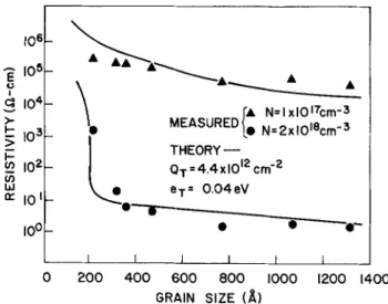
u I c~ 10 4 >- I-.- _~ I 0 3 - l02 W ~ I0 i0 C - A 9 9 N=I xlOITcm-3 MEASURED N=2x 1018cm_ 3 L 9 THEORY - -QT=4.4xlOI2 cm -2 eT= 0.04 eV I I I I I I 0 2 0 0 4 0 0 6 0 0 8 0 0 I000 1200 1400 GRAIN SIZE (~)Fig. 7. Measured and theoretical resistivity v s . average grain size of
different thickness films.
Also, s i n c e Q r c o u l d b e p r e c i s e l y d e t e r m i n e d , t h e v a l u e o f eT w a s a d j u s t e d w i t h i n a r e a s o n a b l e d e g r e e t o p r o d u c e t h e b e s t r e s u l t s o f t h e p vs. L c u r v e s . F i g u r e 7 s h o w s t h e m e a s u r e d r e s i s t i v i t i e s o f d i f f e r e n t t h i c k n e s s f i l m s vs. t h e m e a s u r e d a v e r a g e g r a i n sizes. T h e t h e o r e t i c a l c u r v e s a g r e e w e l l w i t h t h e e x p e r i m e n t a l d a t a a n d e x p l a i n t h e drastic increase of resistivity w i t h d e c r e a s i n g film thickness. B e c a u s e d e c r e a s e of film t h i c k n e s s c a u s e s re- d u c t i o n of grain size, w h e n the grain size r e a c h e s a r o u n d 2 1 0 A at d o p i n g c o n c e n t r a t i o n of 2 • i0 is c m -3, m o s t of the grains go f r o m partial depletion into total depletion, a n d the n u m b e r of free carriers available for c o n d u c t i o n drastically decreases, t h u s c a u s i n g a s h a r p increase of r e s i s t i v i t y . I n c o n t r a s t , a t d o p i n g c o n c e n t r a t i o n o f 2 • 101~ c m 3 for t h e r a n g e o f film t h i c k n e s s s t u d i e d i n t h i s w o r k , m o s t of t h e g r a i n s h a v e b e e n t o t a l l y d e p l e t e d , a n d t h e r e f o r e , t h e c h a n g e s o f r e s i s t i v i t y a r e n o t so d r a s t i c as i n t h o s e s a m p l e s w i t h d o p i n g c o n c e n t r a t i o n o f 2 • 10 TM c m 3. A s a r e s u l t , t h e c a r r i e r t r a p p i n g e f f e c t d u e t o g r a i n - size v a r i a t i o n a t d i f f e r e n t film t h i c k n e s s e s is a d o m i n a n t f a c t o r f o r t h e r e s i s t i v i t y i n c r e a s e i n b o r o n - d o p e d L P C V D p o l y s i l i c o n f i l m s as t h e film t h i c k n e s s de- c r e a s e s (>-1000A). Conclusions T h e e f f e c t o f film t h i c k n e s s o n t h e e l e c t r i c a l p r o p e r t i e s o f b o r o n - d o p e d L P C V D p o l y s i l i c o n f i l m s h a s b e e n s t u d - i e d d o w n to film t h i c k n e s s o f 0.1 /zm. I t h a s b e e n f o u n d t h a t t h e r e s i s t i v i t y i n c r e a s e s e x p o n e n t i a l l y as t h e film t h i c k n e s s d e c r e a s e s , r a t h e r t h a n r e m a i n i n g c o n s t a n t , a n d t h e i n c r e a s i n g r a t e is a s t r o n g f u n c t i o n o f d o p i n g c o n c e n - t r a t i o n . A f t e r a q u a n t i t a t i v e s t u d y of t h e p h y s i c a l m e c h a - n i s m s w h i c h m a y a f f e c t t h e r e s i s t i v i t y as film t h i c k n e s s d e c r e a s e s , t h e c a r r i e r t r a p p i n g e f f e c t d u e to g r a i n - s i z e var- i a t i o n a t d i f f e r e n t film t h i c k n e s s e s w a s s h o w n to b e t h e d o m i n a n t factor. A t r a p p i n g m o d e l w i t h o u t a s s u m i n g t h e d e p l e t i o n a p p r o x i m a t i o n c a n e x p l a i n t h e e x p e r i m e n t a l o b s e r v a t i o n s w e l l a n d e n h a n c e s u n d e r s t a n d i n g o f t h e re- s i s t i v i t y b e h a v i o r as p o l y s i l i c o n film t h i c k n e s s d e c r e a s e s . I t also s h o w s t h a t w h e n t h e p o l y s i l i c o n films are e m - p l o y e d i n V L S I c i r c u i t s , t h e s e n s i t i v i t y o f t h e r e s i s t i v i t y to t h e film t h i c k n e s s m u s t b e c o n s i d e r e d i n t h e d e v i c e de- s i g n (23). Acknowledgments T h e a u t h o r s w i s h to t h a n k t h e g r o u p o f P r o f e s s o r L. J. C h e n o f N a t i o n a l T s i n g - H w a U n i v e r s i t y for h e l p i n g t h e t o p - v i e w T E M s t u d i e s a n d Dr. L . M . T e r m a n of I B M for h e l p f u l c o m m e n t s . T h i s w o r k w a s p a r t i a l l y s u p p o r t e d b y t h e N a t i o n a l S c i e n c e C o u n c i l o f t h e R e p u b l i c o f C h i n a . M a n u s c r i p t s u b m i t t e d Aug. 26, 1983; r e v i s e d m a n u - s c r i p t r e c e i v e d Nov. 28, 1983. T h i s w a s P a p e r 234 pre- s e n t e d at t h e D e t r o i t , M i c h i g a n , M e e t i n g of t h e S o c i e t y , Oct. 17-21, 1982.
I B M T . J . Watson Research Center assisted in m e e t i n g the p u b l i c a t i o n costs of this article.
902 J. Electrochem. Soc.: S O L I D - S T A T E S C I E N C E A N D T E C H N O L O G Y A p r i l 1984 R E F E R E N C E S 1. T. I. K a m i n s , J. Appl, Phys., 42, 4357 (1971). 2. J. Y. W. Seto, ibid., 46, 5247 (1975). 3. T. I. K a m i n s , M. M. M a n d u r a h , a n d K. C. Saraswat, This Journal, 125, 927 (1978).
4. R. D. Rosler. Solid State Technol., 2(), 63 (1977). 5. L. Mei a n d R. W. Dutton, IEEE Trans. Electron. De-
vices, ed-29, 1726 (1982).
6. J. P. Colinge, E. D e m o u l i n , F. D e l a n n a y , M. L o b e t , and J. M. T e m e r s o n , This Journal. 128, 2009 (1981). 7. N. C. C. Lu, L. G e r z b e r g , C. Y. Lu, a n d J. D. Meindl,
IEEE Trans. Electron. Devices, ed-30. 137 (1983). 8. M. G. B u e h l e r , W. R. T h u r b e r , a n d S. D. Grant, This
Journal, 125, 645~ 650 (1978).
9. R. F a l c k e n b e r g , E. Doering, a n d H. Oppolzer, Ab- stract 570, p. 1429, T h e E l e c t r o c h e m i c a l S o c i e t y Ex- t e n d e d Abstracts, L o s A n g e l e s , California, Oct. 14-19, 1979.
10. Y. Wada a n d S. N i s h i m a t s u , This Journal, 125, 1499 (1978).
11. M. A. Frisch, W. Reuter, a n d K. W i t t m a a c k , Rev. Sci. Instrum., 51, 695 (1980).
12. M. E. C o w h e r a n d T. O. S e d g w i c k , This Journal, 119, 1565 (1972).
13. A. L. Fripp, J. Appl. Phys., 46, 1240 (1975).
14. G. B a c c a r a n i , B. Ricco, a n d G. S p a d i n i , J. Appl. Phys., 49, 5565 (1978).
15. N. C. C. Lu, L. Gerzberg, C. Y. Lu, a n d J. D. Meindl, IEEE Trans. Electron. Devices. ed-28, 818 (1981). 16. N. C. C. Lu, L. G e r z b e r g , C. Y. Lu, a n d J. D. Meindl,
I EEE Electron. Devices Lett., edl-2, 95 (1981). 17. M. M. M a n d u r a h , S. C. Saraswat, a n d T. I. K a m i n s ,
IEEE Trans. Electron. Devices, ed-28, 1163 (1981). 18. S. S o l m i , M. Severi, R. A n g e l u c c i , L. Baldi, a n d R.
Bilenchi, This Journal, 129, 1811 (1982).
19. M. M. M a n d u r a h , S. C. Saraswat, C. R. H e l m s , a n d T. I. K a m i n s , J. Appl. Phys., 51, 5755 (1980).
20. W. R e u t e r a n d K. Wittmaack, Appl. Surf. Sci., 5, 221 (1980).
21. K. B o a r d a n d M. Darwish, J. Appl. Phys., 51, 4546 (1980); ibid., 52, 4351 (1981).
22. C. Y. L u a n d N. C. C. Lu, Solid-State Electron., 26, 549 (1983).
23. N. C. C. Lu, L. Gerzberg, a n d J. D. Meindl, IEEE J. Solid-State Circuits, sc-17, 312 (1982).
Polycrystalline Silicon Recrystallization by Combined CW Laser
and Furnace Heating
J. Shappir* and R. Adar
School of Applied Science and Technology, The Hebrew University of Jerusalem, Jerusalem, Israel
A B S T R A C T
A m o d i f i e d CW a r g o n l a s e r - i n d u c e d lateral r e c r y s t a l l i z a t i o n of p o l y c r y s t a l l i n e silicon is d e s c r i b e d . H o l d i n g t h e s a m p l e in a f u r n a c e at e l e v a t e d t e m p e r a t u r e of a b o u t 1000~ r e s u l t e d in significantly r e d u c e d t h e r m a l g r a d i e n t s and stresses. A w i d e r r a n g e of p o w e r is a l l o w e d for p r o p e r r e c r y s t a l l i z a t i o n b o t h on o x i d e a n d s u b s t r a t e areas simulta- neously. P r e f e r r e d t h e r m a l profiles e n a b l e d l a r g e r lateral e p i t a x y of - 5 0 ~ m p e r single scan. T h e h i g h e r s u b s t r a t e t e m - p e r a t u r e r e s u l t e d also in w i d e r m e l t e d areas a n d h i g h s c a n rates of 80 cm/s e n a b l i n g m u c h s h o r t e r p r o c e s s i n g time.
I n r e c e n t years~ i n t e n s i v e effort has b e e n m a d e in differ- e n t t e c h n i q u e s to o b t a i n large area silicon on i n s u l a t o r (SOI) as an a l t e r n a t i v e s u b s t r a t e for i n t e g r a t e d circuits. B e s i d e s t h e o b v i o u s a d v a n t a g e s of r e d u c e d j u n c t i o n ca- p a c i t a n c e , no d e v i c e c o u p l i n g , a n d no c o n t a c t spiking, it can e v e n t u a l l y l e a d to t h r e e - d i m e n s i o n a l i n t e g r a t i o n of e l e c t r o n i c d e v i c e s (1, 2). G a t et al. o b s e r v e d (3) t h a t t h e r e c r y s t a l l i z a t i o n of po]ysilicon layers on an i n s u l a t i n g s u b s t r a t e by a CW laser b e a m r e s u l t s in grains h a v i n g di- m e n s i o n s up to 2 • 25 tLm 2.
I n o r d e r to f a b r i c a t e larger-area S O I s t r u c t u r e s w i t h o u t grain b o u n d a r i e s a n d w i t h c o m p l e t e c o n t r o l of t h e crys- t a l l o g r a p h i c orientation, s e e d e d lateral e p i t a x y t e c h n i q u e has r e c e n t l y b e e n s t u d i e d (4, 5). In this t e c h n i q u e , a re- gion w h e r e t h e p o l y s i l i c o n is in d i r e c t c o n t a c t w i t h t h e sil- i c o n s u b s t r a t e s e r v e s as a s e e d for lateral crystal g r o w t h to t h e a r e a w h e r e t h e p o l y s i l i c o n is o v e r an i n s u l a t i n g layer.
With s t a n d a r d i s o p l a n a r t e c h n o l o g y , lateral e p i t a x y of 20-30 t~m was o b t a i n e d . Modified c o p l a n a r s t r u c t u r e w i t h no step b e t w e e n t h e p o l y s i l i c o n on silicon (PS) a n d poly- silicon on o x i d e (PO) or t h e utilization of t h i n u n d e r l y i n g i n s u l a t o r s (< 1500A) r e s u l t e d in f u r t h e r i n c r e a s e of t h e lat- eral e p i t a x y to 70-80 t~m (5, 6).
I n t h e s t a n d a r d laser r e c r y s t a l l i z a t i o n configurations, t h e silicon w a f e r is a t t a c h e d to a m e t a l c h u c k t h a t can be h e a t e d u p to 700~ (6) and t h e laser b e a m raises t h e layer t e m p e r a t u r e to a b o v e its m e l t i n g p o i n t of 1415~ S u c h an a r r a n g e m e n t suffers f r o m t w o m a j o r d r a w b a c k s : (i) It is difficult to find o p t i m a l recrystallization c o n d i t i o n s for b o t h t h e P S a n d P O areas d u e to t h e d i f f e r e n c e in t h e ver- tical h e a t c o n d u c t i o n in t h e t w o regions, a n d (ii) t h e h i g h lateral t h e r m a l g r a d i e n t s are b o u n d to r e d u c e t h e crystal- line q u a l i t y of t h e r e c r y s t a l l i z e d layer.
*Electrochemical Society Active Member.
Key words: laser annealing, recrystallization, silicon on insula- tor.
To o v e r c o m e t h e s e t w o p r o b l e m s , t h e a p p r o a c h of this w o r k was to raise t h e s u b s t r a t e t e m p e r a t u r e to a b o u t 1000~ b y p l a c i n g it in a d i f f u s i o n f u r n a c e a n d u s e l o w e r laser p o w e r to raise locally t h e p o l y s i l i c o n t e m p e r a t u r e to its m e l t i n g point. In this setup, t h e w a f e r loses m o s t h e a t by b l a c k b o d y r a d i a t i o n r a t h e r t h a n b y t h e r m a l c o n d u c t - a n c e to t h e m e t a l c h u c k .
I n t h e following, certain results of this c o m b i n e d laser a n d f u r n a c e recrystallization t e c h n i q u e are r e p o r t e d .
Experimental
T h e e x p e r i m e n t a l s e t u p c o n s i s t e d of t h e laser, t h e op- tics, t h e s c a n n e r s , a n d t h e furnace, w h e r e t h e w a f e r w a s h e l d d u r i n g t h e r e c r y s t a l l i z a t i o n process. T h e laser was a C o h e r e n t 18W A r i o n laser, o p e r a t e d in t h e m u l t i l i n e m o d e w i t h w a v e l e n g t h s n e a r 0.5 tLm. T h e optical s y s t e m c o n s i s t e d of t w o l e n s e s in a b e a m e x p a n d i n g s t r u c t u r e t h a t s e r v e d b o t h as b e a m e x p a n d e r a n d f o c u s i n g e l e m e n t to o b t a i n an 80 t~m d i a m s p o t size, at a focal d i s t a n c e of 700 ram. T h e b e a m was s c a n n e d across t h e w a f e r b y m e a n s of t w o g a l v a n o m e t e r - d r i v e n mirrors. T h e silicon w a f e r w a s v a c u u m h e l d b y an a d j u s t a b l e q u a r t z t u b e w h i c h e n t e r e d t h e f u r n a c e f r o m its b a c k side. T h e s y s t e m also i n c l u d e d a c o n v e n t i o n a l m e t a l v a c u u m c h u c k for c o m p a r i s o n p u r p o s e s . T h e e x p e r i m e n t a l s e t u p is illus- t r a t e d s c h e m a t i c a l l y in Fig. 1.
T h e 0.5 tLm-thick p o l y c r y s t a l l i n e silicon l a y e r was de- p o s i t e d on a s t a n d a r d i s o p l a n a r structure, o b t a i n e d by lo- cal o x i d a t i o n of t h e p - t y p e <100> silicon s u b s t r a t e to 0.7 a n d 1.1 tLm o x i d e t h i c k n e s s e s . As a stabilizing c a p p i n g layer, u s e was m a d e of C V D - d e p o s i t e d Si3N4 or t h e r m a l l y g r o w n SiO~ layers of v a r i o u s t h i c k n e s s e s . A f t e r t h e recrys- tallization step, t h e c a p p i n g layers w e r e r e m o v e d a n d S e c c o e t c h (7) was u s e d to r e v e a l t h e g r a i n b o u n d a r i e s .
Results
Effects of recrystallization at elevated substrate temperatures.--The m a i n a d v a n t a g e o f t h e recrystalliza-
) unless CC License in place (see abstract).
ecsdl.org/site/terms_use
address. Redistribution subject to ECS terms of use (see
140.113.38.11