使用量子點雷射減慢光訊息行進速度
85
0
0
全文
(2) 使用量子點雷射減慢光訊息行進速度 Slowing Light Using Quantum-Dot Laser Amplifiers 研 究 生:劉瑞農. Student:Jui-Nung Liu. 指導教授:郭浩中. Advisor:Hao-Chung Kuo. 盧廷昌. Tien-Chang Lu. 國 立 交 通 大 學 光 電 工 程 研 究 所 碩 士 論 文. A Thesis Submitted to Institute of Electro-Optical Engineering College of Electrical Engineering and Computer Science National Chiao Tung University in partial Fulfillment of the Requirements for the Degree of Master in Electro-Optical Engineering August 2007 Hsinchu, Taiwan, Republic of China. 中 華 民 國 九 十 六 年 八 月.
(3) 使用量子點雷射減慢光訊息行進速度. 研究生:劉瑞農. 指導教授:郭浩中 教授、盧廷昌 教授. 國立交通大學 光電工程研究所. 摘 要. 本論文旨在探索半導體雷射於作為慢光元件之新穎用途。針對之前 實驗所觀察量子點面射型雷射的慢光現象進行探討,並使用雷射放大器 模型進行理論模擬。模擬結果解釋了光訊息速度隨著雷射增益加大而減 慢,以及隨者調變頻率增高而加快等實驗上觀察到的現象。此外,針對 實驗尚未研究的部份,模擬結果預測了 1 至 5 GHz 的光訊息在該雷射元 件之行進速度。在另一方面,本論文從實驗的角度探索了使用半導體雷 射外部注入光之技術來減慢光資訊速度之可能。利用網路分析儀所量測 到的相位響應顯示有可能達成接近 360 度的 RF 訊號延遲。光譜資料顯 示了這樣的 RF 延遲與光訊息被不對稱的放大有關。. i.
(4) Slowing Light Using Quantum-Dot Laser Amplifiers. Student:Jui-Nung Liu. Advisors:Dr. Hao-Chung Kuo Dr. Tien-Chang Lu. Institute of Electro-Optical Engineering National Chiao Tung University. ABSTRACT. This thesis explores the novel use of semiconductor lasers as optical delay lines.. Slowing light using vertical-cavity surface-emitting lasers (VCSELs). is explained and simulated using the VCSEL amplifier model.. Simulated. results and experimental result are qualitatively in a good agreement.. With. the aid of the filter phase analysis, the simulations explain that group delay increases with increased modal gain and decreases with increased modulation frequency.. Besides, the simulations predict the VCSEL’s. capability of delaying single-tone sinusoidal signal of 1 to 5 GHz.. On the. other hand, RF delay or optical delay using injection-locking of VCSELs is studied experimentally in the thesis.. Optical spectra show that the VCSEL. is not in the stable-locking range.. The VCSEL acts as a regenerative. amplifier, making one of the signal side band much larger than the other.. ii.
(5) ACKNOWLEDGEMENT. 時光飛逝,轉眼間要畢業了。碩士論文能夠順利完成,首先要感謝 郭浩中老師的賞識,賦予我這個挑戰性高、需要量子電子學理論與通訊 實驗技術兩者兼備的研究題目。另外,王興宗老師對於學問研究的熱忱 與毅力,深深地影響我做學問的態度。感謝彭朋群博士在光通訊實驗的 指導與全力協助。感謝盧老師的指導。感謝林俊廷博士與文凱在實驗上 的幫忙。感謝工研院奈米光電中心祁錦雲博士、林國瑞博士與楊泓彬博 士在量子點雷射元件的提供,使我得以一窺奈米技術在光電領域的運 用。此外,感謝李建平老師對我在量子與固態物理學的啟蒙,使我堅信 憑著這股興趣可以讓自己在人生的路上走得更遠,並對社會產生更大的 貢獻。感謝莊順連教授的鼓勵,使我有了靈感與不眠不休的衝勁,因而 得以完成這份論文的主要模擬部份。 感謝實驗室師兄姐:鴻儒、小朱、小強、芳儀、宗鼎、剛帆、志堯、 柏傑、清華、明華、俊榮、士偉、貽安、宗憲與姚忻宏的幫忙與指點。 感謝同學:碩均、金門、孟儒、潤琪、家璞、卓奕與秉寬的扶持。感謝 401 實驗室的學弟妹:晁恩、柏源、伯駿、家銘、昀恬、尚樺的陪伴, 祝你們將來都順順利利的。 最後,要感謝我的家人,你們在背後的支持提供了我克服困難的動 力。. 劉瑞農 新竹交通大學 2007 年秋. iii.
(6) TABLE OF CONTENTS. ABSTRACT (IN CHINESE). i. ABSTRACT (IN ENGLISH). ii. ACKNOWLEDGMENT. iii. LIST OF FIGURES. vii. CHAPTER 1. 1. INTRODUCTION. 2. SEMICONDUCTOR LASERS AND LOW-DIMENSIONAL GAIN MATERIALS. 5. 2.1. Introduction. 5. 2.2. Kane’s k ⋅ p Theory for Semiconductor Band Structure. 5. 2.2.1 2.3. Kane’s k ⋅ p Model with the Spin-Orbit Interaction. 8. Semiconductor Heterostructures and the Effective Mass Theory. 11. 2.4. Quantum Wells, Wires, and Dots. 13. 2.5. Interband Optical Transition and Gain. 17. 2.6. Semiconductor Lasers. 19. 2.7. High-Speed Direct Modulation of Semiconductor Lasers. 27. 2.8. Semiconductor Lasers with Low-Dimensional Gain. 2.9. Materials. 32. Summary. 35. iv.
(7) 3. SLOWING LIGHT USING QUANTUM-DOT LASER AMPLIFIERS. 36. 3.1. Introduction. 36. 3.1.1. Slowing Light with Material Dispersion. 38. 3.1.2. Slowing Light with Waveguide Dispersion and Optical. 3.1.3 3.2. 3.3. 3.4. 4. 5. Resonators. 39. Applicability and Design Issues of Slow-Light Devices. 40. Review of the Previous Experimental Work. 41. 3.2.1. QD-Laser Device Structure. 41. 3.2.2. Experimental Setup. 42. 3.2.3. Measurements of the Group Delay. 44. Theoretical Analysis and Simulation. 46. 3.3.1. Introduction. 46. 3.3.2. Explanation and Simulation. 46 54. Summary. SLOWING LIGHT USING INJECTION-LOCKING OF VCSELS. 55. 4.1. Introduction. 55. 4.2. Introduction to Injection-Locking of Semiconductor Lasers – Rate Equations and Steady-State Analysis. 55. 4.3. Experimental Setup. 57. 4.4. Experimental Results and Discussion. 60. 4.5. Summary. 64. 65. CONCLUSION v.
(8) BIBLIOGRAPHY. 67. APPENDIX Reflection of a Single-Tone Optical Signal from a Photonic Device 72. or a System. vi.
(9) LIST OF FIGURES. CHAPTER 2 Figure 2.1. crystal. Figure 2.2.. Schematic of the periodic potential in a one-dimensional 6 A single-band in the k ⋅ p method.. 7. Figure.2.3. Schematic of the direct gap semiconductor band structure using Kane’s model. The heavy-hole effective mass is corrected in this figure.. 10. Figure 2.4.. 11. Possible three types of semiconductor heterojunctions.. Figure 2.5 Schematic diagrams of the double heterostructure (DH) and the quantum-well heterostructure.. 12. Figure 2.6.. 14. Schematic of the quantum well structure.. Figure 2.7. Schematic of a quantum well having two energy eigenstates, and the energy spectra in the k-space.. 14. Figure 2.8.. 15. Schematic of (a) quantum wire and (b) quantum dot.. Figure 2.9. Schematics of the density of states for bulk materials, quantum wells, quantum wires, and quantum dots.. 17. Figure 2.10. material.. 17. Optical interband transition in a direct gap semiconductor. Figure 2.11. Schematics of a Fabry-Perot resonator with mirror reflectivity R1 and R2. Figure 2.12.. Schematic of an asymmetric Fabry-Perot resonator with a vii. 20.
(10) gain material.. 21. Figure 2.13. (a) A double heterostructure (DH) semiconductor laser and (b) its band structure profile.. 23. Figure 2.14. Schematic of the light power–injection current curve (L-I curve) of a semiconductor laser.. 24. Figure 2.15. Device structure of VCSEL.. 25. Figure 2.16. Cavity mode spectra for (a) edge-emitting laser and (b) VCSEL, and optical gain spectra against frequency.. 25. Figure 2.17.. Calculated reflectivity spectra of the Al 0.9 Ga 0.1 As / GaAs. DBR ( λ Bragg = 1300 nm ) with different number of quarter-wave pairs.. 26. Figure 2.18. Schematic diagram of the direct modulation of semiconductor lasers.. 29. Figure 2.19. Schematic of the modulation spectra of a semiconductor laser at different injection currents.. 31 72. Schematic optical spectra of a single-frequency Figure 2.20. semiconductor laser and a direct modulated single-frequency laser.. 32. Figure 2.21. lasers.. Schematic gain spectra of ideal (a) QW laser and (b) QD 33. CHAPTER 3 Figure 3.1. Schematic drawing of a general photonic transmission system. The box can be an atomic medium, a semiconductor quantum-dot nanostructure, an optoelectronic device, and so on. Figure 3.2.. Schematic diagram of the QD-VCSEL. viii. 36. 42.
(11) Figure 3.3. Light power-injection current curve of the QD-VCSEL [12]. Figure 3.4.. Experimental setup used for group delay measurement.. 42 43. Figure 3.5. Group delay of the 10-GHz sinusoidal signal for injection current I=0.6, 0.7, 0.9, and 1 mA [12].. 45. Figure 3.6. Group delay of sinusoidal signals for 5, 6, 7, 8, 9, and 10 GHz at 1 mA [12].. 45. Figure 3.7. Schematic optical spectrum of the reflection from a VCSEL used to explain the group delay.. 47. Figure 3.8. simulations.. VCSEL amplifier model used to carry out theoretical 48. Figure 3.9. Simulated amplitude response of the VCSEL amplifier for three different modal gain values of 0.7 g th , 0.9 g th , and 0.99 g th .. 50. Figure 3.10. Corresponding simulated phase response of the VCSEL amplifier for the same three different modal gain values.. 50. Figure 3.11. Simulated group delay as a function of modulation frequency for different modal gains. Experimental data is also shown in this figure. 51. Figure 3.12. Simulated group delay as a function of modal gain for different modulation frequencies. 52. CHAPTER 4 Figure 4.1. Experimental setup used for RF delay or optical delay measurement.. 59. Figure 4.2. Light-current curve of the quantum-dot VCSEL used in this study. The threshold current is about 0.8 mA.. 60. ix.
(12) Figure 4.3. Measured relative amplitude response of an injection-locked VCSEL for various wavelength detuning values. The input signal power before entering the VCSEL is -14 dBm throughout the study.. 61. Figure 4.4. Measured corresponding RF phase change response of an injection-locked VCSEL for various wavelength detuning values.. 62. Figure 4.5. Optical spectrum at wavelength detuning of 0.1122nm. Modulation frequency is 14 GHz, corresponding to RF phase change of 200 degree for the wavelength detuning.. 63. Figure 4.6. Modulation. Optical spectrum at wavelength detuning of 0.1386nm. 63. x.
(13) Chapter 1. INTRODUCTION. Semiconductor optoelectronics deals with the interaction between electrons and photons in the semiconductor materials and devices [1, 2].. Form an applied. physicist’s point of view, semiconductor optoelectronics is an exciting application of quantum mechanics. In order to describe how electrons interact with photons, semi classical treatment which treats photons as a perturbation field [3], or all quantum-mechanically approach which sees photons as quanta [2], is needed. Besides, to design semiconductor materials and devices, quantum mechanics is necessary to understand the crystal band structure, quantized electronic quantum states in a low-dimensional nanostructure, and the working principle of the devices. We have witnessed the great impact of the semiconductor optoelectronics on both our everyday lives and scientific interests.. One successful example is the. quantum-well semiconductor laser. Thanks modern heteroepitaxy techniques such as molecular beam epitaxy (MBE) and metal-organic chemical vapor deposition (MOCVD), high-quality quantum-well lasers can be made.. Today, the quantum-well. semiconductor laser is found in virtually every home as part of the compact-disc (CD). 1.
(14) player [4]. On the other hand, the success in the growth of quantum-well structure makes a study of the introductory quantum physics realizable in these artificial semiconductor structures [3].. Semiconductor heterostructures and especially low-dimensional. nanostructures such as quantum wells (QW), quantum wires, and quantum dots (QD), currently comprise the object of investigation of two thirds of all research groups in the physics of semiconductors [4].. Among them, a QD mimics the basic properties. of an atom providing a geometrical size allowing the practical application of atomic physics to the field of semiconductor devices [5].. In the optoelectronics applications,. quantum-dot lasers are expected to show a broader modulation bandwidth, higher temperature stability and lower power consumption than quantum-well counterparts, primarily due to the discrete energy states of electrons and holes under three-dimensional quantum confinement by quantum dots [6].. At the beginning of. the 1990s it was realized that universal self-organization on surfaces in lattice mismatched heteroepitaxial growth can be used to form high densities of homogenous QDs [7]. Recently, owing to the developments of high-density and high-quality InAs-based self-assembled quantum dots, semiconductor lasers using semiconductor quantum dots in the wavelength range of 1.3–1.6µm have improved in their performances remarkably [6].. Therefore, QD lasers are very promising for new. generations of edge-emitting lasers (EEL) and vertical-cavity surface-emitting lasers (VCSEL) in communication.. 2.
(15) In addition to the development of the semiconductor lasers with low-dimensional gain materials, one of the remaining grand challenges in optoelectronic technology is the ability to store an optical signal in optical format [8].. Slow light, i.e. optical. signal propagating at a velocity much slower than the speed of light in the vacuum, has attracted unprecedented attentions in the past few years [9].. Various. mechanisms have been used to obtain a large material dispersion for achieving slow light on semiconductor platform [8, 9]. Among these methods, slowing light using quantum-well Fabry-Perot laser [10], quantum-well VCSEL [11], and quantum-dot VCSEL [12] creates new application of semiconductor lasers in communication in addition to serving as optical transmitters.. Especially, large delay-bandwidth. product (DBP) using surface-emitting lasers are experimentally demonstrated [11, 12], but few theoretical explanation and analysis are given. The outline of this thesis is as follows. y. Chapter 2 gives an introduction to semiconductor optoelectronics and semiconductor lasers. y. Chapter 3 first reviews the previous experimental work in [12] and subsequently utilizes VCSEL amplifier model to explain this novel slow-light phenomenon with VCSEL.. y. Chapter 4 studies RF delay or optical delay using injection-locking technique of semiconductor lasers.. y. The last chapter concludes the research study, and presents some future. 3.
(16) work.. 4.
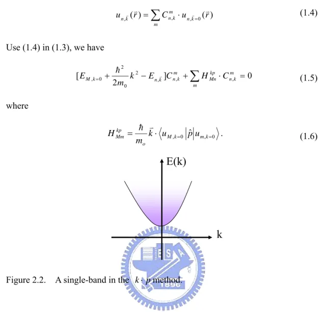
(17) Chapter 2. SEMICONDUCTOR LASERS AND LOW-DIMENSIONAL GAIN MATERIALS. 2.1 INTRODUCTION In this chapter, the basic theory of the semiconductor band structure using Kane’s. k⋅p. model. and low-dimensional nanostructures will be reviewed first.. Subsequently, electron-photon interaction in semiconductors and its low-dimensional structures will be described using semi-classical approach. Then we will review one of the most important device applications of semiconductor optoelectronics – semiconductor lasers, and vertical-cavity surface-emitting lasers (VCSELs) will then be addressed.. Afterward, semiconductor lasers with low-dimensional gain materials. will be discussed.. 2.2 KANE’S k ⋅ p THEORY FOR SEMICONDUCTOR BAND STRUCTURE [3, 13, 14] A semiconductor crystal has a periodic arrangement of the atoms, and then has a v v v v periodic electronic potential V (r ) = V (r + T) , where T is the translational vector of 5.
(18) the crystal lattice.. Fig. 2.1 shows schematic plot of the periodic potential in a. one-dimensional crystal.. V(x) T=ma,. m=±1, ±2, ±3,…. +. +. +. +. x. Cryatal ions. a. Figure 2.1. Schematic periodic potential in a one-dimensional crystal.. To describe the behavior of an electron in the semiconductor crystal, we must solve the eigenstates of the time-independent Schrödinger equation: 2 ˆ ψ ( rv ) v = [ − h ∇ 2 + V ( rv )]ψ v = E v ⋅ψ v ( rv ) . H n,k n ,k n,k n,k 2m 0. (1.1). Besides, for an electron in a periodic potential, Bloch theorem requires that. v. v. vv. ψ n ,kv (r ) = u n ,kv (r ) ⋅ e ik ⋅r .. (1.2). Therefore, the Schrödinger equation can be rewritten as [−. h2 h v v h 2k 2 v v ∇ 2 + V (r ) + k ⋅ p ]u n ,kv = ( E n , kv − ) ⋅ u n ,kv ( r ) 2m 0 m0 2m0. At the zone center (k=0), we can solve the energy eigenstates.. (1.3). Because the. Hamiltonian operator is hermitian, the eigenstates not in the zone center can be presented as the linear combination of the eigenstates at the zone center. Using the eigenstates at the zone center as the basis, we can get. 6.
(19) v v u n ,kv ( r ) = ∑ C nm,k ⋅ u n ,kv = 0 ( r ). (1.4). m. Use (1.4) in (1.3), we have [ E M ,k =0 +. h2 2 kp k − E n ,kv ]C nm,k + ∑ H Mn ⋅ C nm,k = 0 2m0 m. (1.5). where kp H Mm =. h v k ⋅ u M ,k =0 pˆ u m ,k =0 . mo. (1.6). E(k). k. Figure 2.2. A single-band in the k ⋅ p method.. For a single band, such as the band edge of conduction band (Fig. 2.2), using (1.3) and the time-independent perturbation theory to the second order, we can get. v 2 k ⋅ un,k =0 pˆ un',k =0 v hk h h − = En,k =0 + k ⋅ un,k =0 pˆ un,k =0 + 2 ⋅ ∑ 2m0 m0 m0 n'≠n En,kv=0 − En',kv=0 2 2. En,k. 2. (1.7) Therefore, we can have. E n ,kv − E n ,kv =0 = D αβ =. D αβ ⋅ kα ⋅ k β ∑ α β , = x, y, z. h2 1 h2 h2 δ α ,β + ( )α ,β = 2 2 m* 2m0 2m0 7. Pnnα ' ⋅ Pnnβ ' + Pnnβ ' Pnnα ' ∑ E v −E v n '≠ n n ,k =0 n ', k = 0. (1.8). (1.9).
(20) where Pnn ' is the momentum matrix element. According to (1.8), the eigen-energy near the band edge is in the quadratic form.. 2.2.1 Kane’s k • p Model with the Spin-Orbit Interaction. If the spin-orbit interaction is taken into account, we add a spin-orbit interaction term in the Hamiltonian.. Because spin-orbit interaction perturbation is proportional to. L ⋅ S , where L and S are the orbit angular momentum and the spin angular momentum,. respectively. Thus, we have the total Hamiltonian H=−. h2 2 h2 2 v ∇ + V (r ) + λ ( J − L2 − S 2 ) . 2m0 2. (1.10). Use this total Hamiltonian and the Bloch theorem, the Schrödinger equation becomes [−. h2 2 h 2k 2 h2 h v v v v ∇ 2 + V (r ) + k ⋅ p+λ ( J − L2 − S 2 )]u n , kv = ( E n ,kv − ) ⋅ u n , kv ( r ) . 2m 0 m0 2 2m0. (1.11) At the zone center, [−. h2 h2 2 v v ∇ 2 + V (r ) + λ ( J − L2 − S 2 )]u n ,kv = 0 = E n , kv = 0 ⋅ u n , kv = 0 ( r ) . 2m 0 2. (1.12). The solutions of the above equation form a complete set, so we can expand the eigenstate not in the zone center as the linear combination of the complete set at zone center. Because the total angular momentum J, the orbit angular momentum L, the spin angular momentum S, and L ⋅ S coupling term commute with each other, they can have common complete set of eigenfunctions. Since s=1/2 for electron, we can denote the eigenstates of these operators as 8. j, m j , l. in Dirac notation, where the.
(21) items in the “ket” are the quantum numbers corresponding their physical operators. ˆ S =E S Assume H 0 s. ˆ j = 1, m = E j = 1, m , and choose the basis and H 0 j p j. functions. iS ↑ , iS ↓ , Z ↑ , Z ↓ , X − iY 2. ↑ ,−. X − iY. ↓ ,−. 2. X + iY 2. ↑ ,. X + iY 2. ↓. .. (1.13). Then we can have an 8x8 interaction matrix ⎡. [H] = ⎢ H ⎣⎢ 0. 0⎤ ⎥ H ⎦⎥. (1.14). v where, assuming k = kzˆ is in the z-direction, the 4x4 matrix H is 0 ⎡Es ⎢ ∆ ⎢ 0 Ep − 3 ⎢ H=⎢ 2∆ ⎢kP 3 ⎢ ⎢0 0 ⎣. kP 2∆ 3 Ep 0. ⎤ ⎥ 0 ⎥ ⎥ ⎥ 0 ⎥ ∆⎥ Ep + ⎥ 3⎦. 0. (1.15). where P = −i. is the Kane’s parameter, and ∆ = 3. λh 2 2. h S Pˆz Z m0. (1.16). .. Solving the eigenvalue problem. [H] - E'⋅I = 0 , we can obtain the energy eigenvalues near the zone center:. 9. (1.17).
(22) Ec = Eg + E hh =. 2 ∆) h 2k 2 3 (Conduction band, C) = Eg + E g ( E g + ∆) 2mc *. k 2 P 2 (Eg +. h2k 2 (Heavy - hole band, HH) 2 m0. E lh = −. (1.18). .. 2k 2 P 2 h2k 2 (Light - hole band) =3E g 2mlh *. (1.19) (1.20). k 2P2 h 2k 2 E so = − (Split - off band) = −∆ − 3( E g + ∆ ) 2m so. (1.21). Note that the conduction band effective mass increase with increased band gap of a semiconductor material. The Kane’s model indicates positive effective mass for heavy-hole band, and this is corrected in the Luttinger-Kuhn model [3, 14, 15].. E(k) Conduction band. Eg k Heavy-holes band Light-holes band. Spin-orbit band. Figure.2.3. Schematic band structure of the direct gap semiconductor using Kane’s model. The heavy-hole effective mass is corrected in this figure.. The Kane’s model is summarized in Fig. 2.3. The heavy-hole effective mass is corrected in the figure.. 10.
(23) 2.3. SEMICONDUCTOR. HETEROSTRUCTURES. AND. THE. EFFECTIVE MASS THEORY In the previous section, we assumed the semiconductor crystal is infinite. Practically, useful semiconductor optoelectronic devices usually have small size, and are the combination of several semiconductor materials of different band structures (semiconductor heterostructures).. When two semiconductors of different band. structures are joint, a heterojunction will then forms. heterojunctions possible (Fig. 2.4).. There are three types of. Furthermore, semiconductor heterostructures. important to optoelectronics such as the double heterostructure (DH) and the quantum well are shown in the Fig. 2.5. DH is used in the early semiconductor lasers before quantum-well lasers are invented.. Ec. Ev. Type 1. Type 2. Figure 2.4. Possible three types of semiconductor heterojunctions.. 11. Type 3.
(24) Ec. Ev. . Figure 2.5.. Quantum well. Double heterostructure. Schematic diagrams of the double heterostructure (DH) and the. quantum-well heterostructure.. Now, we then need a general theory to describe how an electron behaves in these optoelectronic materials. For the single-band case, the variation of the band stucture with the position can be treated as a perturbation on the Hamiltonian.. If this. perturbation is slowly varying, then the behavior of an electron in semiconductors can be described as the effective mass theory (EMT) or envelop function approximation (EFA) [3, 14, 15] [−. h2 1 v v v ∇ ∇ + U (r )]F (r ) = ( E − E n ,kv =0 ) F (r ) . 2 m*. (1.22). where m* is the electron effective mass, U is the perturbation energy function seen by an electron, E n ,k =0 is the band-edge energy.. v v v where ψ (r ) = F (r ) ⋅ u n ,k =0 (r ) .. v F (r ) is the envelope function,. Note that (1.22) is very similar to the standard. time-independent Schrödinger equation. For DH, the thickness of the small-band gap region is much larger than the electron’s deBroglie wavelength, so the quantum effect is negligible.. Classical. semiconductor device physics can then be used to analyze the band structure of DH. 12.
(25) [3]. For quantum well, the small-band gap region width is comparable to the electron’s deBroglie wavelength, and obvious quantum effect will then occur. Theory of the quantum wells will be addressed in the next section.. 2.4. QUANTUM WELLS, WIRES, AND DOTS. Low-dimensional structure is an artificial structure that provides one-dimensional to three-dimensional quantum effect.. Therefore, the width of the low-dimensional. structure and the electron deBroglie wavelength must be in the same order. Because the conduction band effective mass in direct gap semiconductor materials such as InAs and GaAs is usually much smaller than the vacuum electron mass, low-dimensional semiconductor quantum structures have scale in several tens to hundreds of nanometers, rather than the smaller size of a natural atom. We use effective mass theory to accurately describe the behavior of an electron in a low-dimensional semiconductor structures, or semiconductor nanostructures, termed because the electron deBroglie wavelength in a semiconductor is nanoscale.. 13.
(26) y. Barrier. x. Well Barrier. z. Lz. 0. Figure 2.6. Schematic diagram of the quantum well structure.. Energy. Energy U(z) 2. 1. 0. Lz. 0. z. K. Figure 2.7. Schematic diagram of a quantum well having two energy eigenstates, and the energy spectra in the k-space.. For an electron in an one-dimensional (1D) semiconductor nanostructure, or a quantum well (QW) (Fig. 2.6), the envelope function can be expressed as the product of three components v v v Fwell (r ) = e iK ⋅R ⋅ F ( z ). (1.23). v v v v where K = k x xˆ + k y yˆ , and R = x + y . After substitution and assuming the effective. 14.
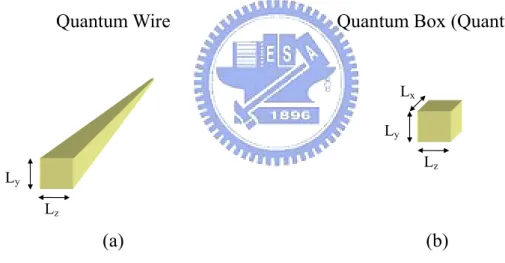
(27) mass is the same in the different materials, the energy eigenvalues of this standard quantum-mechanics problem are En =. v h2K 2 * 2mwell. 2. + εn. (1.24). where the eigenenergy ε n satisfies [-. 1 ∂ h2 ∂ + U(z)] Fn (z) = ε n ⋅ Fn (z) . 2 ∂z m * (z) ∂z. (1.25). The equation can be solved easily by use of graphical solution method, similar to the rectangular slab waveguide problems. Fig. 2.7 shows schematic of a quantum well having two energy eigenstates, and the energy spectra in the k-space.. Quantum Wire. Quantum Box (Quantum Dot). Lx Ly Lz. Ly Lz. (a). (b). Figure 2.8. Schematic diagrams of (a) quantum wire and (b) quantum dot.. Likewise, quantum wires (Fig. 2.8a) and quantum boxes (or quantum dots, QD) (Fig. 2.8b)are two-dimensional (2D) and three-dimensional (3D) nanostructures, respectively.. The effective mass equation can be easily solved using separable. variable method.. 15.
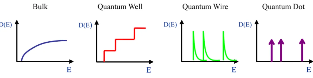
(28) For quantum wires, v Fwire (r ) = e ik x x ⋅ F ( y ) ⋅ F ( z ). (1.26). v U wire ( r ) = U(y) + U(z). (1.27). En = [-. [-. h2kx. 2. * 2m well. 2. + εn + εm. 1 ∂ h2 ∂ + U(z)] Fn (z) = ε n ⋅ Fn (z) 2 ∂z m * (z) ∂z. h2 ∂ 1 ∂ + U(y)] Fm (y) = ε m ⋅ Fm (y) . 2 ∂y m * (y) ∂y. (1.28) (1.29). (1.30). For quantum boxes,. [-. v Fbox (r ) = F ( x) ⋅ F ( y ) ⋅ F ( z ). (1.31). v U box ( r ) = U ( x) + U(y) + U(z). (1.32). En = ε l + ε n + ε m. (1.33). h2 ∂ 1 ∂ + U(z)] Fn (z) = ε n ⋅ Fn (z) 2 ∂z m * (z) ∂z. (1.34). h2 ∂ 1 ∂ [+ U(y)] Fm (y) = ε m ⋅ Fm (y) 2 ∂y m * (y) ∂y. (1.35). h2 ∂ 1 ∂ [+ U(x)] Fl (x) = ε l ⋅ Fl (x) . 2 ∂x m * (x) ∂x. (1.36). With the knowledge of the quantum states, it is useful to calculate density of state (D.O.S) D(E), which is defined as the number of quantum states per unit volume between E and E+dE. Schematic diagrams of the density of states of bulk materials, quantum wells, quantum wires, and quantum dots are plotted in Fig. 2.9.. 16.
(29) Bulk. Quantum Well. Quantum Wire. D(E). D(E). Quantum Dot. D(E). E. D(E). E. E. E. Figure 2.9. Schematic diagrams of the density of states for bulk materials, quantum wells, quantum wires, and quantum dots.. 2.5 INTERBAND OPTICAL TRANSITION AND GAIN [2, 3] We now have a brief review the optical transition in bulk and low-dimensional nanostructures. If the electron-hole system is subjected to a sinusoidal steady-state electromagnetic perturbation (Fig. 2.10), then the optical transition will be possible. E(k) Conduction band. hν Eg k. Valence band. Figure 2.10. Optical interband transition in a direct gap semiconductor material.. In quantum mechanics, time-dependent perturbation theory and the Fermi’s golden rule tell us in order to have an optical transition between a state in the conduction. 17.
(30) band and a state in the valence band, the transition energy difference must equal to the photon energy (∆E=hν) and the k-selection rule must be obeyed (kc≈kv).. The. transition probability, or transition rate, is proportional to the optical matrix element v v H'ba = b − er ⋅ E a. (1.37). where a and b denote the wave function of the two states. Using slowly-varying approximation and the Bloch theorem, we can have v eA v v b − er ⋅ E a ≅ − 0 eˆ ⋅ Pcv ⋅ δ kc ,kv 2m0. (1.38). where Pcv is the interband momentum matrix element, eˆ is the unit directional vector of the electric field and A0 is the amplitude of the vector potential. The gain coefficient g is defined as the fraction of photons increased per unit distance:. g=. 1 dS ( z ) 1 dI ( z ) = S dz I dz. (1.39). where S is the photon density and I is the light intensity. For a bulk semiconductor, assuming the conduction band is completely empty, and the valence band is completely full, then gain coefficient of the bulk semiconductor is v 2 πe 2 ˆ g bulk (hν ) = ⋅ e ⋅ P cv ⋅ Dr (hv − E g ) ⋅ ( f c − f v ) 2 n r cε 0 m 0 ω. (1.40). where fc and fv are the Fermi-Dirac distribution for the electronic state and hole state, respectively. Dr is the density of state using the reduced effective mass 1 1 1 = + . m r me * m h *. (1.41). Note that the gain coefficient is positive if fc>fv (population inversion). At this time, 18.
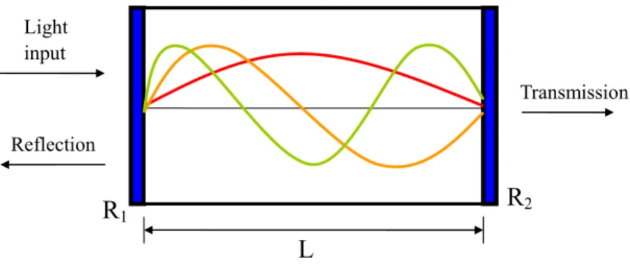
(31) the light in the material will be amplified. For a low-dimensional semiconductor nanostructure, and assuming the valence band-mixing effect is negligible, and there is only one quantized state in each of the conduction and valence band, the gain coefficient is g low -dimensional (hν ) =. v 2 2 πe 2 en ⋅ I eh eˆ ⋅ Pcv ⋅ Drl (hv − E g ) ⋅ H (hv − E hm ) ⋅ ( fc − fv ) 2 n r cε 0 m 0 ω (1.42). where E he = E g + E e − E h. is the interband transition energy.. (1.43). Because the density of states spectra of the. low-dimensional nanostructures is sharper and higher than that of the bulk semiconductors, the max gain achievable where lasing behavior usually occur is higher in low-dimensional nanostructures than in bulk materials. This characteristic opens the applications of the low-dimensional nanostructures in optoelectronics, termed “nano-photonics”.. 2.6 SEMICONDUCTOR LASERS [1, 2] Semiconductor lasers are important optoelectronic devices.. Applications of the. semiconductor lasers include optical storage, optical communication, medical use etc. Before we discuss how semiconductor lasers can be used to slow down optical information velocity, it is beneficial to have a brief review on the basic properties of the Fabry-Perot resonators. 19.
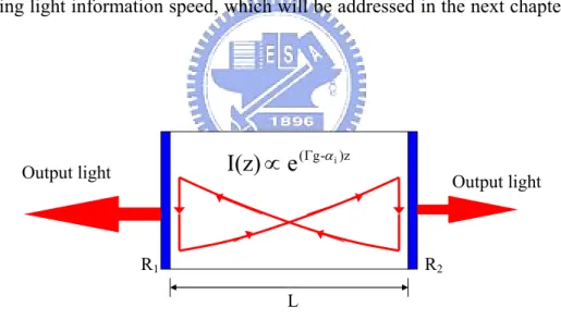
(32) Light input Transmission Reflection. R2. R1 L Figure 2.11.. Schematic illustration of a Fabry-Perot resonator with mirror. reflectivity R1 and R2.. A Fabry-Perot resonator (Fig. 2.11) consists of two planar mirrors of reflectivity R1 and R2.. Assuming lossless mirrors and no mirror phase shift, the electric field. transmission coefficient t and the electric field reflection coefficient r of the Fabry-Perot resonator are as follow [1]: t1 ⋅ t 2 '⋅ exp[−i. 2πnL. ]. λ0 t= 4πnL 1 − r1 '⋅r2 '⋅ exp[−i ] λ0 r1 + r2 '⋅ exp[−i. 2πnL. (1.44). ]. λ0 r= 4πnL 1 − r1 '⋅r2 '⋅ exp[−i ] λ0. (1.45). where r1, r1’, r2, r2’, t1, t1’, t2, t2’ are reflection and transmission coefficients of the mirrors.. The intensity transmission coefficient T and the intensity reflection. coefficient R of the Fabry-Perot resonator are defined as the square of the absolute value of t and r, respectively.. 20.
(33) From (1.44), the t is unity if 2L = m ⋅. λ0. (1.46). n. where m is any integer. On the other hand, r is zero also whenever 2L = m ⋅. λ0 n. .. (1.47). Optical wavelengths fulfilling this resonant condition are called Fabry-Perot cavity modes.. It is worthwhile noting that the condition t=1 and r=0 is the resonant. transportation of the photon, which has its counterpart in the electronic device examples. Furthermore, the phase of the t and r has its profound significance for use in slowing light information speed, which will be addressed in the next chapter of the thesis.. I(z) ∝ e ( Γg-α i )z. Output light. Output light. R2. R1 L. Figure 2.12.. Schematic diagram of an asymmetric Fabry-Perot resonator with a gain. material.. If the resonator includes a gain material (An active resonator), then the story will be more interesting. Fig. 2.12 shows schematic of an asymmetric Fabry-Perot resonator with a gain material. The electric field transmission coefficient becomes 21.
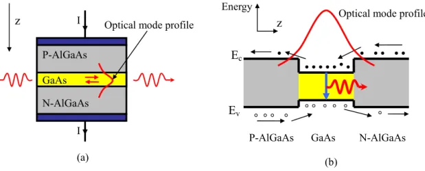
(34) t1 ⋅ t 2 '⋅ exp[−i. t=. 2πnL. ] ⋅ exp[. ( Γg − α i ) L] 2. λ0 4πnL 1 − r1 '⋅r2 '⋅ exp[−i ] ⋅ exp[(Γg − α i ) L] λ0. (1.48). According to (1.48), t will be infinite if Γg th = α i + α m = α i +. 1 ⎛ 1 ln⎜ 2 L ⎜⎝ R1 R2. ⎞ ⎟⎟ ⎠. Gain condition. (1.49). and 2L = m ⋅. λ0 n. Phase condition. (1.50). where Γ is the optical confinement factor. (1.49) is the threshold condition of the lasers.. When above threshold, the gain coefficient of the gain material will clamp at. the threshold value because of the mechanism of gain saturation [1, 2].. Extra. carriers will rapidly recombine and produce photons in the lasing cavity mode. In a semiconductor laser, electrons in conduction band and holes in valence band can recombine and produce photon emission.. In order to control flow of the carriers,. a forward biased p-n junction is generally used in a semiconductor laser. Besides, optical waveguides are needed in order to provide optical confinement and hence can reduce optical loss. In a double heterostructure (DH) semiconductor laser (Fig. 2.13), the central GaAs region provides both the carrier confinement and optical confinement because of the conduction and valence-band profiles and the refraction index profile [3].. 22.
(35) Energy. z. I. Optical mode profile. z. Optical mode profile. Ec. P-AlGaAs GaAs N-AlGaAs. Ev. I. P-AlGaAs. (a). GaAs. N-AlGaAs. (b). Figure 2.13. (a) A double heterostructure (DH) semiconductor laser and (b) its band structure profile.. Light output power of semiconductor lasers when above its lasing threshold can be shown as Pout =. hv α m ⋅ηi ⋅ ( I − I th ) e αi + α m. (1.51a). where ηi is the internal quantum efficient, defined as the percentage of the injected carriers that contribute to the radiative recombination.. The external quantum. efficiency η e is defined as dPout 1 1 ln( ) . η e = dI = η i L R hv 1 1 α i + ln( ) e L R. (1.51b). Fig. 2.14 shows schematic diagram of the light power–injection current curve (L-I curve) of a semiconductor laser.. 23.
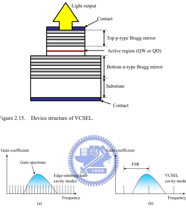
(36) Light power. 0. Figure 2.14.. Ith. Current. Schematic diagram of the light power–injection current curve (L-I. curve) of a semiconductor laser.. Free spectrum range (FSR) of the Fabry-Perot resonator is defined as the separation between neighboring cavity modes in the frequency spectrum, or. FSR = v m +1 − v m =. c . 2nL. (1.52). In order to have a single-frequency laser, FSR need to be large enough compared with gain spectrum.. According to (1.52), to have large FSR, the cavity length L must be. small. Compared with the long cavity length of a edge-emitting semiconductor laser such as the double heterostructure semiconductor lasers and the quantum-well Fabry-Perot lasers, vertical-cavity surface-emitting lasers (VCSELs) (Fig. 2.15) have cavity length of several optical wavelength. Thus, VCSEL is an ideal candidate for the single frequency semiconductor lasers. Fig. 2.16 shows the cavity mode spectra for edge-emitting laser (EEL) and VCSEL, and optical gain spectra against frequency.. 24.
(37) Light output Contact. Top p-type Bragg mirror Active region (QW or QD) Bottom n-type Bragg mirror. Substrate. Contact. Figure 2.15. Device structure of VCSEL.. Gain coefficient. Gain coefficient Gain spectrum. FSR VCSEL cavity modes. Edge-emitting laser cavity modes. Frequency. Frequency (a). (b). Figure 2.16. Cavity mode spectra for (a) edge-emitting laser and (b) VCSEL, and optical gain spectra against frequency.. However, because short cavity length induces large mirror loss, making high-reflectivity laser mirrors and then decreasing mirror loss becomes a critical issue of VCSEL. Distributed Bragg reflectors (DBRs) consist of alternating layers of dielectric or semiconductor materials.. The difference in the index of refraction. 25.
(38) between adjacent layers give rise to a high reflectivity (>99%) at the vicinity of the Bragg frequency [1]. The thickness of each layer is λ0 /(4n) , where n is the index of refraction of the layer [1]. At the Bragg wavelength, the reflectivity of the DBR is given by [16]:. R max DBR. ⎛ ⎛n ⎜1− ⎜ L ⎜ ⎜n =⎜ ⎝ H ⎜ ⎛ nL ⎜ 1 + ⎜⎜ ⎝ ⎝ nH. ⎞ ⎟⎟ ⎠. 2p. ⎞ ⎟⎟ ⎠. 2p. where p is the number of the quarter-wave pairs.. ⎞ ⎟ ⎟ ⎟ ⎟ ⎟ ⎠. 2. (1.53). nH is the larger refraction index,. while nL stands for the smaller one. The reflectivity spectra of the DBRs can be calculated using transfer matrix method. Fig. 2.17 shows the calculated reflectivity spectra of the DBRs with different number of quarter-wave pairs.. DBR Reflectivity 1.0. 25 pairs. 0.8. 0.6. 0.4. 0.2. 1. µ 10-6. 1.1 µ 10-6. 1.2 µ 10-6. 1.3 µ 10-6. 26. 1.4 µ 10-6. 1.5 µ 10-6. l H mL 1.6 µ 10-6.
(39) DBR Reflectivity 1.0. 15 pairs. 0.8. 0.6. 0.4. 0.2. 1. µ 10-6. 1.1 µ 10-6. 1.2 µ 10-6. 1.3 µ 10-6. 1.4 µ 10-6. 1.5 µ 10-6. l H mL 1.6 µ 10-6. DBR Reflectivity 1.0. 10 pairs. 0.8. 0.6. 0.4. 0.2. 1. µ 10-6. Figure 2.17.. 1.1 µ 10-6. 1.2 µ 10-6. 1.3 µ 10-6. 1.4 µ 10-6. 1.5 µ 10-6. l H mL 1.6 µ 10-6. Calculated reflectivity spectra of the Al 0.9 Ga 0.1 As / GaAs DBR. ( λ Bragg = 1300 nm ) with different number of quarter-wave pairs.. 2.7 HIGH-SPEED DIRECT MODULATION OF SEMICONDUCTOR LASERS [1-3] Optical communication is one of the most important applications of the semiconductor lasers. A unique feature of semiconductor lasers is that, unlike other lasers that are modulated externally, the semiconductor laser can be modulated 27.
(40) directly by modulating the injection current [1]. This is especially important in view of the possibility of monolithic integration of the two principle actors of the modern information era—the transistor and the laser—in integrated semiconductor optoelectronic circuits [1]. Light output power of the Semiconductor lasers is proportional to (I-Ith). Therefore, if the injection current has a dc component and a small signal sinusoidal modulation: I(t) = I 0 + i (t ) = I 0 + im (ω )e jωt J(t) = J 0 + j (t ) = J 0 + jm (ω )e jωt N(t) = N 0 + n(t ) = N 0 + nm (ω )e jωt. (Current) (Current density) (Carrier density). (1.54) (1.55) (1.56). then we would expect that the light output power will correspondingly be with a dc component and a small signal sinusoidal modulation terms .. P(t) = P0 + p(t ) = P0 + pm (ω )e jωt. (Light output power). S(t) = S0 + s (t ) = S0 + sm (ω )e jωt. (Photon density).. (1.57) (1.58). Then we can transform electrical signal into optical format (Fig. 2.18)by use of semiconductor lasers, and then transmit information optically.. 28.
(41) Power Optical signal output. time. I. 0. Electrical signal input. time. Figure 2.18. Schematic diagram of the direct modulation of semiconductor lasers.. To have a review on the basic theory of the direct modulation of semiconductor lasers, let us start from the carrier density (N) and photon density (S) rate equation: N dN J = − v ⋅ g (N ) ⋅ S − τ dt ed. (1.59). dS S = Γ ⋅ v ⋅ g (n ) ⋅ S − + β sp Rsp dt τp. (1.60). Where β sp is the spontaneous emission factor, τ is the carrier lifetime, and Rsp is the spontaneous emission rate per unit volume.. ⎛c = ⎜⎜ τ p ⎝ nr 1. τ p is the photon lifetime. ⎞ ⎡ 1 ⎛ 1 ⎞⎤ ⎟⎟⎥ . ⎟⎟ ⋅ ⎢α i + ln⎜⎜ 2 L R R ⎝ 1 2 ⎠⎦ ⎠ ⎣. (1.61). Assuming there is only one lasing mode, and using linear gain approximation. g (N ) = g 0 + g ' (N − N 0 ) Where g' is the differential gain at I=I 0 , in addition to small Signal approximation:. J 0 >> J m 29. (1.62).
(42) N 0 >> nm. (1.63). S 0 >> s m , then it can be shown that. ⎡ ⎤ ⎢ ⎥ ⎛ j m (ω ) ⎞ Γτ p ω r2 s m (ω ) = ⎢ ⎟ ⎥ ⋅⎜ 1 ed 2 2 ⎝ ⎠ ⎢ − jω ( + S 0 ⋅ v ⋅ g ' ) − ω + ω r ⎥ ⎢⎣ ⎥ τ ⎦. (1.64). where. ⎛ S0 ⎞ ⎟. ⎟ τ p ⎝ ⎠. ω r2 = vg ' ⎜⎜. (1.65). And. fr =. ωr 1 ⎛ ∂g ⎞ v ⋅⎜ = ⎟ 2π 2π ⎝ ∂N ⎠ N. is the relaxation frequency. Modulation. M (ω ) =. s m (ω ) = jm (ω ). 0. ⎛S ⋅⎜ 0 ⎜τ ⎝ p. frequency. Γτ p ω r2 ed. 1 jω ( + S 0 ⋅ v ⋅ g ' ) − ω 2 + ω r2. τ. =. Γτ p. ⎞ ⎟ ⎟ ⎠. response. (1.66) M (ω ). is:. ω r2. 1/2 ed ⎡ 2 1 2 2 2 2⎤ ⎢ω (τ + S 0 ⋅ v ⋅ g ' ) − (ω - ω r ) ⎥ ⎦ ⎣ (1.67). which peaks at ω = ω r . Given that the photon lifetime in a typical semiconductor laser is about several pico-seconds, differential gain is of the order of 10 -6 cm 2 , photon density is about 1015 photons / cm 3 , the modulation frequency or modulation bandwidth is about. 30.
(43) several GHz.. The high-speed modulation ability and the compact volume make. semiconductor lasers an ideal candidate for signal transmitter in optical electronics. Increasing injection current increases the light output, and then increases the relaxation frequency.. Fig. 2.19 shows schematic plot of modulation spectra at different injection. currents.. Modulation response I = I1 I = I2 > I1. Modulation frequency Figure 2.19.. Schematic plot of the modulation spectra of a semiconductor laser at. different injection currents.. A very important concept, but people are usually ignorant, is that the optical spectrum of a modulated single-frequency semiconductor laser is not longer single-frequency.. When subjected to a sinusoidal direct modulation, the photon. number in the laser cavity and the light output power is modulated. Hence, the amplitude of the electric field of the laser light is also modulated. amplitude modulation (AM) scheme.. This is the. The electric field under AM can be easily. shown [17]:. 31.
(44) E(t) = E 0 (1 + m sin[ω m t ]) sin[ω c t ] = E 0 sin[ω c t ] +. m m E 0 cos[(ω c − ω m )t ] − E 0 cos[(ω c + ω m )t ] 2 2. (1.68). Where m is the modulation index, ω c is the carrier frequency, and ω m is the modulation frequency.. Schematic optical spectra of the direct modulated. single-frequency laser are shown in the Fig. 2.20. Optical spectrum. Optical spectrum Carrier LSB USB. fc. Frequency. Frequency. fm fm. Figure 2.20. Schematic optical spectra of a single-frequency semiconductor laser and a direct modulated single-frequency laser. (LSB: Lower side band. USB: upper side band, fm: modulation frequency, fc: carrier frequency). 2.8 SEMICONDUCTOR LASERS WITH LOW-DIMENSIONAL GAIN MATERIALS A semiconductor laser with low-dimensional gain materials is superior to its counterpart with bulk gain materials, or double-heterostructure (DH) lasers. Because of the discrete energy eigenstates, gain spectra of the low-dimensional nanostructures are narrower than bulk materials. As a result, injected carriers can. 32.
(45) effectively increase the population inversion within a narrower spectra width. This characteristic makes lasers with low-dimensional gain material can have larger differential gain and smaller threshold current densities than conventional DH semiconductor lasers. Thus, lasers with low-dimensional gain material can have larger modulation relaxation frequency and larger available modulation bandwidth as compared with DH lasers. Compared with QW gain materials, ideal QD have very sharp density of states. The gain spectrum of an ideal QD material is narrowly centered on its transition energy. Therefore, based on the laser theory, it is easier and quicker to reach threshold gain in an ideal QD laser than in an ideal QW laser. Besides, the lasing wavelength of the lasers with low-dimensional gain material is less sensitive to the injection current, because of the narrower gain spectra. Fig. 2.21 shows schematic plots of the gain spectra of the ideal QW and QD lasers. Ideal QW gain spectrum. Gain coefficient. Gain coefficient Ideal QD Gain spectrum. Cavity modes. E. e1 h1. = E e1 + E g − E h1. Energy. (a). Energy (b). Figure 2.21. Schematic gain spectra of ideal (a) QW laser and (b) QD lasers.. Modern crystal growth techniques such as the molecular beam epitaxy (MBE) and the metal-organic chemical vapor deposition (MOCVD), has demonstrated that it is 33.
(46) possible to grow semiconductors of different atomic compositions on top of another semiconductor substrate with monolayer precision [3].. Therefore, high-quality. quantum-well gain materials can be made by utilizing these epitaxy techniques. Since the mid-1990s, there has been considerable work on the direct synthesis of semiconductor nanostructures by applying the phenomenon of island formation during strained-layer heteroepitaxy, a process called the Stranski-Krastanow growth mode [16].. During the heteroepitaxial growth, the semiconductor atoms tend to form. islands spontaneously on a planar wetting layer because the strain energy can be relaxed and is energetically favorable there. If these islands are small enough to have quantum effect, they are called self-assembled quantum dots. Due to the much higher number of available states in the 2-D wetting layer and barrier states at high temperatures, compared to that in the dots, injected carriers preferably occupy the wetting layer and barrier states [18]. This makes the carrier dynamics of the real quantum dots dependent not only on the QD discrete levels, but also on the wetting layer and barrier states. Besides, the QD size non-uniformity during the spontaneous self-organized process can causes the ground-state (GS) optical transition energies of the quantum dots vary from one QD to another and hence broaden the gain spectrum, so the real GS optical gain spectrum of QD is not an ideal delta function. These difficulties limit the performances of today’s QD lasers. In the thesis, we will study the slow-light phenomenon in a self-organized QD laser, whose QD active region is fabricated by use of MBE technique.. 34.
(47) 2.9 SUMMARY In this chapter, the basic theory of the semiconductor band structures using Kane’s. k ⋅ p model and the low-dimensional nanostructures is reviewed. Subsequently, electron-photon interaction in semiconductors and its low-dimensional structures is described using semi-classical approach. semiconductor lasers.. Then we review the basics of. Finally, semiconductor lasers with low-dimensional gain. materials and their challenges are discussed.. 35.
(48) Chapter 3. SLOWING LIGHT USING QUANTUM-DOT LASER AMPLIFIERS. 3-1 INTRODUCTION [1, 8-11, 19-34] The reduction in light group velocity, termed “slow light”, has been a fast-moving topic. recently,. with. communications [19].. potential. applications. from. quantum. computing. to. Before the study of the slow-light using semiconductor. lasers, a brief review of the important definitions and terms would be helpful. Referring to Fig. 3.1, we consider the transmission of an input light signal x(t) through a general photonic system, and the output light signal is y(t).. Photonic material,. x(t). device, or system. y(t). H(ω). Figure 3.1. Schematic drawing of a general photonic transmission system.. The. box can be an atomic medium, a semiconductor quantum-dot nanostructure, an optoelectronic device, and so on.. 36.
(49) If the photonic “box” is a linear time-invariant system, in the frequency domain, the output Fourier transform Y(t) is the product of the input Fourier transform X(t) and the frequency response of the photonic “box”, and this relationship can be written Y (ω ) = H (ω ) ⋅ X (ω ). (3.1). Typically H(ω) is complex, which we will write as H (ω ) = H (ω ) ⋅ e − iφ (ω ) , where H (ω ) is the amplitude response and φ (ω ) is the phase response.. If the amplitude. response is uniform over the optical regime of the input light signal and the higher-order terms in phase response can be neglected, the output signal remains identical to that of the input signal, with a time delay of (dφ / dω ) . Thus the propagation time delay, referred to as the group delay, due to propagation through the photonic box plotted in Fig. 3.1 is given by. τ=. dφ dω. (3.2). which is, in general, a function of frequency. If the physical length of the photonic box is L, then the group velocity in the box can be defined L. vg =. τ. .. (3.3). Besides, the slowdown factor S is S=. c vg. which is equivalent to the definition of the group index n g .. 37. (3.4).
(50) 3.1.1 Slowing Light with Material Dispersion. When the photonic box is an optical material, we have. φ (ω ) =. ω c. n(ω ) ⋅ L .. (3.5). Here, n(ω) is the frequency-dependent refraction index of the material, and L is the length of the material. Applying (3.2), we find that. τ= where group index n g = n(ω ) + ω. L c / ng. (3.6). dn in this case. So the group velocity of the light dω. signal in the photonic material can be written vg =. L. τ. =. c. (3.7). dn n(ω ) + ω dω. To obtain a very slow light group velocity, we can increase the material index n(ω) and/or the material dispersion. dn . However, it is hard to change the material index, dω. because it is related to the inherent absorption/gain spectra by the famous Kramer-Kronig relation.. Though producing a sharp dip in the gain/absorption. spectra, the material dispersion can be very large, based on Kramer-Kronig relation. Various mechanisms have been used to obtain a large material dispersion for achieving slow light [8, 9, 21]. These include electromagnetically induced transparency (EIT) [22, 23], coherent population oscillations (CPOs) or four-wave mixing (FWM) in atomic crystals [24] and semiconductor optical amplifiers [25-29], etc. 38.
(51) While having a very large slowdown factor, EIT needs a long dephasing time, so that the quantum coherent interference between the quantum energy levels is not destroyed.. This makes EIT impossible to be achieved at room temperature.. Compared with EIT, CPO is less sensitive to the dephasing effect, so it may be used as the basis of the room-temperature slow-light devices. To increase the bandwidth in a CPO medium, semiconductor-based materials has been proposed because of its longer carrier lifetime (~1 ns) than atomic crystals (~ms).. With the discrete energy. levels and the stronger carrier confinement, recent experiments have been successful using CPO or FWM in QW and QD devices from low to room temperatures [27-29].. 3.1.2 Slowing Light with Waveguide Dispersion and Optical Resonators. In addition to material dispersion, slow-light can also be achieved by utilizing structurally dispersive resonators. Recently, group delay of 110-140 ps of a 200 MHz sinusoidal signal in a coupled ring optical waveguide (CROW) has been experimentally demonstrated [30].. However, the delay in a passive CROW or a. passive resonator is not tunable. Chuang et al varied the group delay by changing the injection current of a quantum-well Fabry-Perot laser amplifier [10] and a semiconductor DFB-phase-shifted coupled cavity [31, 32].. Besides, slowing light. using photonic crystal defect cavities has also been experimentally demonstrated [33]. In addition the experiment, designing of a resonator slow light device is an interesting issue.. Designing coupled-resonator optical waveguide delay line has. 39.
(52) been proposed using transfer matrix, tight-binding, and time domain formalisms, and these points of view are consistent with one another [34]. Among these theoretical analysis tool, transfer matrix approach is particularly enabling because it can deal with any arbitrary sequence of resonator [34].. On the other hand, Chuang et al uses. transfer matrix method to analyze the phase response of the coupled cavity under various current injection [31, 32].. With this information, they can predict group. delay of a sinusoidal signal, and then reshape the waveform of the delayed pulse train. These successful designing tools largely increase the practicability of the slow light devices with dispersive resonators.. 3.1.3 Applicability and Design Issues of Slow-Light Devices [11, 31, 32]. While both material and structurally dispersive method offer unique features, it is important to evaluate them in terms of their applicability to delay line. For a practical tunable optical delay line, one would require [31, 32] 1.. Continuously tunable group delay via an external control mechanism, which may be electrical, optical, or even mechanical.. 2.. Minimal power variation accompanying change in delay. 3.. Of useful bandwidth. This is the key towards implementations of compact optical delay line because broadband signals in the GHz-range are required in most communications applications [11].. 4.. Compactness and suitability to integration into optoelectronic platforms.. 40.
(53) 5.. Room-temperature operation.. 3.2 REVIEW OF THE PREVIOUS EXPERIMENTAL WORK [12] 3.2.1 QD-Laser Device Structure [12, 35]. The device used in this study is a quantum-dot vertical-cavity surface-emitting laser (QD-VCSEL) and is depicted in Fig. 3.2. The device structures were fabricated using molecular beam epitaxy (MBE) by NL Nanosemiconductor GmbH (Germany), grown on (100) plane of the GaAs substrates. The top mirror is a 22-pair carbon-doped p+-Al0.9Ga0.1As/p+-GaAs distributed Bragg reflector. (DBR),. and. the. bottom. mirror. is. a. 33.5-pair. Si-doped. n+-Al0.9Ga0.1As/n+-GaAs DBR. In order to increase the electrical conductivity of DBRs, Carbon and Silicon of relatively high concentration about 2-3×1018 cm-3 is used as the p-type dopant in the top DBR and n-type dopant in the bottom DBR respectively, which can result in absorption in the DBRs and hence limit the maximum achievable mirror reflectivity. The length of the undoped graded-index separate confinement heterostructure (GRINSCH) optical cavity was 3λ, without taking DBR penetration depths into account. The active region is composed of five quantum-dot groups. Each group has three layers of quantum dots, and is located within the locations of the intracavity intensity distribution maximum, inset between two linear-graded AlxGa1-xAs (x = 0 to 0.9 and x. 41.
(54) = 0.9 to 0) confinement layers. The light-current curve of the QD-VCSEL is shown in Fig. 2.3. The details of the device structure were described in [35]. Light output Contact. P-type Al0.9 Ga0.1 As / GaAs DBR (22 pairs) InAs QD active region N-type Al0.9 Ga0.1 As / GaAs DBR (33 pairs). GaAs substrate Contact. Figure 3.2. Schematic diagram of the QD-VCSEL.. 10000. Power (nW). 8000 6000 4000 2000 0 0.0. 0.2. 0.4. 0.6. 0.8. 1.0. Injection Current (mA). Figure 3.3. Light power-injection current curve of the QD-VCSEL [12].. 3.2.2 Experimental Setup. Our experimental setup for optical delay measurement is shown in Fig. 3.4. 42.
(55) CW. TLD. M-Z. Mod.. VA. PC. OC DUT. RF. Coupler RF Source. Splitter. OSA. Signal. PD. RFA. High-Speed Scope Trigger. Optical path Electrical path. Figure 3.4. Experimental setup used for group delay measurement. (TLD: tunable laser diode; VA: variable attenuator; PC: polarization controller; OC: optical circulator; OSA: optical spectrum analyzer; PD: photodetector; RFA: RF amplifier; DUT: device under test, which is the QD-VCSEL in this study).. The 1300-nm tunable laser diode produces the continuous-wave (CW) probe light. A sinusoidal light signal is then generated after the CW probe light is sent through a Mach-Zehnder interferometric waveguide electro-optical modulator [1-3], which is driven by an RF source. A variable optical attenuator is used to control the power of the light signal, which is fixed to -14 dBm (~40 µW ) in this study. A polarization controller (PC) is used to adjust the polarization of the input light signal. The carrier frequency of the input light signal is adjusted to the QD-VCSEL resonance frequency. The resonance wavelength of the QD-VCSEL is determined by observing directly on 43.
(56) the optical spectrum analyzer (OSA).. We measure the signal group delays by. estimating the scope traces directly. The group delay reference was taken for an input light signal well away from the QD-VCSEL resonance, which is logical because the reflective phase response is flat.. 3.2.3 Measurements of the Group Delay. Measurements at several QD-VCSEL injection current are studied. The amplified spontaneous emission (ASE) center frequency below threshold and the lasing frequency of the QD-VCSEL above threshold are recorded first on the spectrum analyzer. Signal group delay increases when we increase the injection current. Group delay of the 10-GHz sinusoidal signal for various injection currents are shown in Fig. 3.5. For a 10-GHz sinusoid, the maximum group delay of 41 ps at 1 mA is observed. When injection current is 1mA, delay of sinusoidal signals for 5, 6, 7, 8, 9, and 10-GHz are plotted in Fig. 3.6.. 44.
(57) 50. Group delay (ps). 45. 10-GHz. 40 35 30 25 20 15 10 0.5. 0.6. 0.7. 0.8. 0.9. 1.0. 1.1. Current (mA) Figure 3.5. Group delay of the 10-GHz sinusoidal signal for injection current I=0.6, 0.7, 0.9, and 1 mA [12].. Group Delay (ps). 80 1 mA. 70 60 50 40 30. 5. 6. 7. 8. 9. 10. Modulation Frequency (GHz) Figure 3.6. Group delay of sinusoidal signals for 5, 6, 7, 8, 9, and 10 GHz at 1 mA [12].. 45.
(58) 3.3 THEORETICAL ANALYSIS AND SIMULATION 3.3.1 Introduction. Slow-light using quantum-well Fabry-Perot laser [10], quantum-well VCSEL [11], and the quantum-dot VCSEL [12] have been experimentally demonstrated. In [12], the tunable delay of sinusoidally modulated light signal up to 10 GHz is achieved. However, clear physical mechanism and explanation why there is such a high-bandwidth delay in vertical-cavity laser, is rarely provided. On the other hand, delay of 1 GHz sinusoidally modulated signal in a vertical-cavity semiconductor optical amplifier (VCSOA) is studied [36], and a Fabry-Perot model is used to explain the experiment result.. Since the filter phase response changes very fast in the. vicinity of the cavity resonance frequency, the group delay theory in [36] is suitable only for use in the low modulated frequency (<1 GHz) signal, rather than the possible several GHz range bandwidth use of the semiconductor slow-light optoelectronic devices. Chuang et al [31, 32] used transfer matrix formalism to analyze delay of signal of several GHz in a semiconductor active waveguide, and can reshape square waves of 5-GHz bandwidth. In this study, we adopt the approach similar to [31, 32] to analyze slow-light in active vertical-cavity optoelectronic devices.. 3.3.2. Explanation and Simulation. The experimental results with stress on the group delay, injection current, and modulation frequency can be explained by use of VCSEL amplifier model [37].. 46.
(59) Schematic optical spectrum of the reflection from a VCSEL used to explain the group delay is shown in Fig. 3.7. The input signal power in the experiment is -14 dBm or 40 µW , which is much larger than the laser emission power of 8.5 µW of the QD VCSEL biased at 1 mA. The strong input light increases the photon number inside the laser cavity, and then expedites stimulated emission rate of the laser medium, thus depleting the carrier density to a level that is below its lasing threshold [37]. Therefore the VCSEL acts like an amplifier at this time [37]. To explain why group delay increases with the injection current and its trend as a function of modulation frequency, the VCSEL amplifier model is used to carry out some simulations using equivalent Fabry-Perot etalon method [15]. The VCSEL amplifier model used to carry out theoretical simulations is depicted in Fig. 3.8. Optical Power. Carrier wave. Lower side band. Upper side band Reflection from a VCSEL amplifier. Frequency. Figure 3.7. Schematic optical spectrum of the reflection from a VCSEL used to explain the group delay.. 47.
(60) Optical spectrum. λ. λ. Input signal. Output signal. Top DBR Active region Bottom DBR. Substrate. Figure 3.8. VCSEL amplifier model used to carry out theoretical simulations.. The maximum achievable reflectivity of top and bottom DBRs is about 99.65% and 99.66% respectively [16], due to a relatively high doping ( N a , N d = 2 ~ 3 × 1018 cm -3 ) and then considerable absorption optical losses. An input light signal is incident on an active VCSEL resonator below its lasing threshold. The filter phase and the intensity response are the quantities of interests.. Because phase shift of the. distributed Bragg mirror is zero at the Bragg frequency and a slowly-changing linear function in the vicinity of Bragg frequency [1], the mirror phase shift can be neglected. The thickness of the center region Lc is 3 λ, where λ is the laser wavelength in the cavity. The top and bottom DBR penetration depths are calculated and are 1.5 λ respectively. The effective cavity length Lceff is thus 6 λ in the QD VCSEL. The internal loss in the device of 10 cm -1 is assumed in the simulations.. 48. The reflection.
(61) coefficient of the asymmetric Fabry-Perot etalon is [3]: − i 2 kL. ceff r + r2 ⋅ e r = 1 − i 2 kL ceff 1 − r1 ⋅ r2 ⋅ e. (3.8). where r1 and r2 are the real reflection coefficient of the effective top and bottom mirror respectively, k = 2πνne / c + i ( g − α i ) / 2 is the complex propagation constant, where c is the light speed in the air, ne is the effective index of the graded-index separate confinement heterostructure (GRINSCH) active region, g is the modal gain, and α i is the intrinsic internal loss. The reflection intensity response and the phase shift of the resonator are r (ν ). 2. and φ (ν ) = Arg[r ]] , respectively. Fig. 3.9 and Fig. 3.10 show the simulated intensity response and the corresponding phase response of the VCSEL amplifier for three different modal gain values. When g = 0.7 g th , the amplitude response is flat, behaving as an all-pass filter [10]. Note that phase response changes slowly when 0.7 g th increases to 0.8 g th , and then becomes steeper swiftly when modal gain is close to threshold.. 49.
(62) Intensity Response. 100 0.7 gth 0.9 gth 0.99 gth. 10. 1 -40. -20. 0. 20. 40. Frequency Detuning (GHz). Figure 3.9. Simulated amplitude response of the VCSEL amplifier for three different modal gain values of 0.7 g th , 0.9 g th , and 0.99 g th .. Filter Phase (rad.). 10. 0.7 gth 0.9 gth 0.99 gth. 8 6 4 2 -40. -20. 0. 20. 40. Frequency Detuning (GHz). Figure 3.10. Corresponding simulated phase response of the VCSEL amplifier for the same three different modal gain values. 50.
(63) The group delay of an optical sinusoidal signal, given by τ fm = [φ(ν0 + fm ) −φ(ν0 − fm )]/(4π fm ) , can be deduced from the slope of the phase response [32], where f m is sinusoidal modulation frequency of the input light signal. The proof of the formula is in the appendix. Simulated delay as a function of modulation frequency between 1 and 10 GHz for different modal gains is plotted in Fig. 3.11. To have a comparison between simulation results and experimental results, experimental results for injection current 1 mA is also shown in Fig. 3.11. Fig. 3.12 shows the simulated delay as a function of modal gain for different modulation frequencies.. 400. Group Delay (ps). 300. 0.7 gth 0.9 gth 0.95 gth 0.99 gth Experimental data. 200. 100 90 80 70 60 50 40 30. 1. 2. 3. 4. 5. 6. 7. 8. 9. 10. Modulation Frequency (GHz) Figure 3.11.. Simulated group delay as a function of modulation frequency for. different modal gains. Experimental data is also shown in this figure. 51.
(64) 400. Group Delay (ps). 300. Modulation Frequency 1 GHz 2 GHz 3 GHz 5 GHz 10 GHz. 200. 100 90 80 70 60 50 40 30. 18. 19. 20. 21. 22. 23. 24. -1. Modal Gain (cm ). Figure 3.12.. Simulated group delay as a function of modal gain for different. modulation frequencies. The simulation results agree well with the experimental results. The group delay decreases with the increased modulation frequency. This is because phase response changes fast in the vicinity of etalon resonance frequency (phase slope is large), and phase slope is small when the modulation frequency is large. On the other hand, group delay increases with the increased modal gain, because the phase response becomes steeper. Note that the calculated delay of the single-tone 1-GHz signal can be high up to 240 ps, corresponding to a delay-bandwidth product (DBP) [8] of 0.24. Larger simulated DBP of 0.37 can be for the single-tone 10-GHz signal, which is slightly smaller than the experimental value of 0.41.. 52.
(65) If the -14 dBm strong input light signal makes the slave laser below its lasing threshold, spectrum hole burning effect will appear, making index and gain coefficient dependent on wavelength. Our simulation does not take this wavelength-dependent gain into consideration as in [38]. Moreover, because gain value and refraction index of the laser medium are coupled to each other through famous Kramer-Kronig relation, this decrease in gain value can shifts the cavity resonance frequency to a longer wavelength (red-shift).[2, 40].. It can be shown that the amount of this. red-shift frequency change is directly proportional to the linewidth enhancement factor of the laser gain medium [40, 41]: ∆f =. αe 2. vg ⋅ (g s − g 0 ). (3.9). where α e is the linewidth enhancement factor or α-parameter, v g is the group velocity of light in the laser cavity, g s is the suppressed modal gain of the VCSEL, and g 0 is the small-signal modal gain of the VCSEL. It has been predicted that quantum-dot (QD) lasers, in principle, should exhibit a near-zero α-parameter, due to the discrete density of states and symmetric gain spectrum [18]. Our simulation assumes that the carrier frequency is exactly in the VCSEL cavity mode, and should be in best agreement with the experiment when the input signal power is not large enough to change the resonance frequency. On the other hand, we think that four wave mixing (FWM) effect is not obvious in the experiment. Because the large DBR mirror reflectivity, the short cavity length in the VCSEL and the fact that the carrier wave and the signal sidebands cannot be in the 53.
(66) VCSEL cavity mode concurrently, the superposition of the multiple reflected waves can be destructive interference if it is not in the cavity mode.. Consequently,. nonlinear coherent interaction between light of different wavelength such as FWM or coherent population oscillation (CPO) can be negligible in the study. The simulation shown here is done assuming the carrier frequency is in the cavity mode exactly and strong input light signal causes the slave laser below its lasing threshold. Red-shift resonance and the influence of the spectrum hole burning effect need to be included to fully realize the physical mechanism. These are beyond the scope of this master degree thesis and complete investigation is underway.. 3.4 SUMMARY In this chapter, slowing light using vertical-cavity surface-emitting lasers (VCSELs) is explained and simulated using VCSEL amplifier model. Simulated results and result are qualitatively in a good agreement. With the aid of the filter phase analysis, the simulation explains that group delay increases with increased modal gain. Besides, the simulations predict the slow-light capability of delaying single-tone sinusoidal signal of 1 to 5 GHz. Further, the principle should not be suitable for use in VCSELs only. It can be generalized to the general kinds of semiconductor lasers.. 54.
(67) Chapter 4. SLOWING LIGHT USING INJECTION-LOCKING OF VCSELS. 4.1 INTRODUCTION In this chapter, we will study RF delay or optical delay in a semiconductor laser far above its lasing threshold.. This is a standard laser injection-locking problem.. Before any experimental study is described, it is worthwhile reviewing the basic theory of the injection-locking of the semiconductor lasers first.. 4.2 INTRODUCTION TO INJECTION-LOCKING OF SEMICONDUCTOR LASERS – RATE EQUATIONS AND STEADY-STATE ANALYSIS [39-42] When an external laser light (master laser) enter into the resonator of a following laser (slave laser), the behavior of the photon and the carrier in the semiconductor lasers can be described by use of the rate equation formalism below:. 55.
(68) photon :. d 1 1 E SL = { jω + [ g ⋅ v g − ]} ⋅ E SL (t ) + η ⋅ f d ⋅ E ML (t ) τp dt 2. d N (t ) carrier : N=J− − g ⋅ v g ⋅ E 0 (t ) 2 τsp dt. (4-1) . (4-2). In these equations, ESL, EML, and N are the slave laser electric field, the master laser electric field, and the carrier density in the slave laser’s active region, respectively. g is the differential gain. τp and τsp are the photon and carrier lifetimes, respectively. Fd is the longitudinal mode spacing, and η is the coupling coefficient. To solve these united differential equations, we can set: E SL (t ) = E 0 (t ) ⋅ e i (ω0t +φ0 (t )). η ⋅ E ML (t ) = E1 ⋅ e i (ω t ). (4-3). 1. After substitution into the rate equation, we can get. ω - ω0 =. 1 ⋅ α ⋅ v g ⋅ ( g s − g th ) 2. (4-4). (4-5). where α is the linewidth enhancement factor (α-parameter). Because gain coefficient and refraction index of the gain materials are coupled to each other, changing in gain can lead to shift of the cavity resonance. Using (4-3) ~ (4-5), the photon rate equation can then be converted to the amplitude-phase format 1 d E 0 (t ) = v g g ( N − N th ) ⋅ E 0 (t ) + f d ⋅ E1 ⋅ cos[∆ω ⋅ t − φ 0 (t )] 2 dt E 1 d φ 0 (t ) = v g g ( N − N th ) + f d ⋅ 1 sin[∆ω ⋅ t − φ0 (t )] 2 E 0 (t ) dt. (4-6) (4-7). where ∆ω = ω1 − ω 0 is the angular frequency detuning between the free-running lasers. After some algebra derivations, and assuming the steady locking state, the. 56.
(69) depleted carrier density can be shown f E ~ ∆N i = −2 d ⋅ ~1 ⋅ cos(φ L ) v g ⋅ g E0. (4-8). ~ where φ L is the phase of the slave laser with respect to the master laser, and E 0 is. the constant slave laser electric field amplitude.. The light intensity within the. resonator can easily be shown. ~ ( E0 ) 2 =. τ ~ ~ (E 0s ) 2 − p ⋅ ∆N i τs ~ 1 + τ s ⋅ τ p ⋅ ∆N i. (4-9). The stable locking range, where the slave laser and the master laser operate in the same wavelength, can be shown [1985 JQE Henry & Dutta] E E − f d ⋅ ~1 1 + α 2 < ω1 − ω 0 < f d ⋅ ~1 E0 E0. (4-10). From this equation, the stable locking range is wide when the intensity of the master laser is much larger than the slave laser. Besides, the appearance of the α-parameter make the stable locking range not symmetric with respect to the free-running slave laser frequency. Outside the stable locking range, complex nonlinear phenomena such as chaos, four wave mixing, and nonlinear dynamics etc will appear, which are above the scope of this thesis.. 4.3 EXPERIMENTAL SETUP In this study we explore a slow light scheme using an injection-locked semiconductor laser. We demonstrate that the RF delay or optical delay can largely increase due to. 57.
(70) the amplified signal sideband. Fig. 4.1 shows the experimental setup. The 1.3-µm tunable laser diode produces the continuous-wave (CW) probe light. A sinusoidal light signal is then generated after the CW probe light is sent through a Mach-Zehnder interferometric waveguide electro-optical modulator, which is driven by a vector network analyzer (HP 8270ES). variable optical attenuator is used to control the power of the light signal, which is fixed to -14 dBm (~40 µW ) in this study. A polarization controller (PC) is used to adjust the polarization of the input light signal. The input light signal enters the slave semiconductor laser through an optical circulator (OC). A small part of the output light signal enter an optical spectrum analyzer (OSA), and the greater part of the output light signal goes into the photodetector and transforms into electrical RF signal. The RF signal is amplified by a RF amplifier and then goes into the network analyzer. The RF amplitude frequency response and phase frequency response of the output signal are directly observed by measuring the amplitude and the phase response of the S21 port of the network analyzer, calibrated with the responses when the input light signal is away from the free-running slave semiconductor laser wavelength.. Amplitude response and phase response are measured at various. wavelength detuning values (∆λ = λcarrier wave of input – λfree-running slave).. 58.
(71) TLD. CW. M-Z. Mod.. VA. PC. OC DUT. RF. Network Analyzer. RFA. PD. Signal. Coupler. OSA. Optical path Electrical path. Figure 4.1. Experimental setup used for RF delay or optical delay measurement. (TLD: tunable laser diode; VA: variable attenuator; PC: polarization controller; OC: optical circulator; OSA: optical spectrum analyzer; PD: photodetector; RFA: RF amplifier; DUT: device under test, which is the quantum-dot VCSEL in this study).. The slave semiconductor laser used in this study is a monolithically single-mode quantum-dot (QD) vertical-cavity surface-emitting laser (VCSEL) [35].. Fig. 4.2. shows the light-current curve of the slave quantum-dot VCSEL used in this study. In the study, the injection current of the slave VCSEL is 1.7 mA, which is well above its lasing threshold.. 59.
數據


+7

相關文件
(a) A special school for children with hearing impairment may appoint 1 additional non-graduate resource teacher in its primary section to provide remedial teaching support to
volume suppressed mass: (TeV) 2 /M P ∼ 10 −4 eV → mm range can be experimentally tested for any number of extra dimensions - Light U(1) gauge bosons: no derivative couplings. =>
(a) The magnitude of the gravitational force exerted by the planet on an object of mass m at its surface is given by F = GmM / R 2 , where M is the mass of the planet and R is
We explicitly saw the dimensional reason for the occurrence of the magnetic catalysis on the basis of the scaling argument. However, the precise form of gap depends
Let T ⇤ be the temperature at which the GWs are produced from the cosmological phase transition. Without significant reheating, this temperature can be approximated by the
incapable to extract any quantities from QCD, nor to tackle the most interesting physics, namely, the spontaneously chiral symmetry breaking and the color confinement..
• Formation of massive primordial stars as origin of objects in the early universe. • Supernova explosions might be visible to the most
Given a connected graph G together with a coloring f from the edge set of G to a set of colors, where adjacent edges may be colored the same, a u-v path P in G is said to be a
