三族氮化物微結構之成長與光電特性量測
100
0
0
全文
(2) 三族氮化物微結構之成長與光電 特性量測 The Growth and Characterization of Group III-nitride Microstructures 研 究 生:李 寧. Student:Ling Lee. 指導教授:陳衛國博士. Advisor:Prof. Wei-Kuo Chen. 國 立 交 通 大 學 電子物理研究所 博 士 論 文 A Thesis Submitted to Institute of Electrophysics College of Science National Chiao Tung University in partial Fulfillment of the Requirements for the Degree of Doctor of Philosophy in Electrophysics July 2008 Hsinchu, Taiwan, Republic of China. 中華民國九十七年七月.
(3) 三族氮化物微結構之成長與光電特性量測 研究生:李寧. 指導教授:陳衛國博士. 國立交通大學電子物理研究所. 中文摘要 本論文初期我們利用巨觀及微觀角度的電性量測設備探討對於氮化鎵表 面微結構對於薄膜電性的影響。首先利用矽原子調制摻雜技術,我們已能將氮化 鎵表面延伸錯位(threading dislocation)密度降低至 108 cm-2 的水準,在低錯位密度 情況下顯示室溫電子遷移率可以從 57cm-2/V-s 提升至 322 cm2/V-s。藉由分析變溫 霍爾量測所顯示電子遷移率隨溫度變化的趨勢,我們發現高錯位密度情況電子遷 移率主要受限於帶電的延伸錯位。而當錯位密度降低時,電子遷移則主要受限於 點缺陷所形成的短距散射中心(shirt-range scattering center)。除此之外,利用導電 原子力顯微鏡(C-AFM)分析氮化銦表面之 V 型缺陷(V-defect)及平坦處的電流分 布,我們發現 V 型缺陷側壁的電流強度遠較平坦處高約三個數量級以上,電流電壓關係顯示在平坦處的電子傳導機制主要受限於表面氧化層阻擋電流,而在 V 型缺陷側壁由於表面氧化層較薄,電子傳導則是遵照蕭特基(Schottky)傳導機制。. 本論文另外提出「流量調制磊晶法」(FME)及「成長中斷模式」(growth interruptions)用以成長氮化銦奈米結構。在 600℃利用 FME 模式成長氮化銦時, 三族和五族交替通入反應腔,而當通入 TMIn 反應氣體時加入 250sccm 的 NH3 背景流量。實驗顯示當五族通入階段的 NH3 流量大於 1500sccm 後,PL 發光峰 值位於 0.75eV 而譜峰寬度約 75 meV。除此之外,隨著增加五三比由 10000 增加 至 60000 氮化銦等效厚度固定於大約 25 奈米,有別於於傳統磊晶模式當五三比 超過 30000 時成長速度下降至原先的 1/4。我們認為利用 FME 成長模式在高流量 I.
(4) 的 NH3 環境下可以抑制氮原子形成錯位(stacking fault),因此不但不會抑制氮化 銦成長速度,發光強度亦不受 NH3 流量增加而降低。. 最後,我們利用重複次數的「成長中斷模式」(growth interruptions)在 700℃ 成長出無金屬銦顆粒(In droplet)的氮化銦微結構。可以成功地解決氮化銦難以在 高溫成長的困難。實驗結果顯示,當每次截斷 TMIn 供應而保持 NH3 通入的時間 超過 15 秒,重複 45 次之後表面不但沒有金屬銦顆粒存在,PL 發光譜峰也由 0.75eV 降低至 0.7 eV。這個結果據我們所知已不遜於世界級的水準。利用時間解 析光譜量測所顯示低溫載子侷限能量大約 12meV,超過一般量測約 5 至 10 meV 的侷限能量,同時我們亦觀測到有少量金屬銦(In clusters)被包覆於於氮化銦微結 構內。進而推測利用成長中斷模式於高溫製備氮化銦可能在被包覆的銦周圍形成 的受體銦空缺(In vacancy),此能階極有可能主導 0.70eV 的發光行為。. II.
(5) The Growth and Characterization of Group III-nitride microstructures Student:Ling Lee. Advisor:Prof. Wei-Kuo Chen. Institute of Electrophysics National Chiao Tung University. Abstract This thesis elucidates the macroscopic and microscopic electrical properties of the GaN epilayer. First, Si-modulation doping layers (Si-MDLs)are used to reduce the dislocation density to less than 108 cm-2 and improve electron mobility to 322 cm2/V-s Analysis of temperature-dependent mobilities indicates in the high dislocation regime, the electron transport is limited by charged threading dislocations. In the low-dislocation regime, electrons more easily collide with point defects as short-range scattering centers. The consistency between the estimated density and that determined by deep level transient spectroscopy (DLTS) reveals that the short-range scattering centers may be nitrogen interstitial with an energy level at EC-1.01±0.09 eV. On the other hand, conductive atomic force microscopy reveals the spatially resolved current distribution around a V-defect. The current intensity in the V-defect is three orders of magnitude higher than in the surrounding regions. Further static current-voltage measurement suggests that the current flow is governed by Schottky emission and Fowler-Nordheim tunneling in the V-defect region and in the surrounding area, III.
(6) respectively.. Flow-rate modulation epitaxy (FME) is utilized herein to fabricate InN nanostructures. At 600℃ with low background NH3 flows of 250 sccm during the In step with an NH3 flow rate that exceeds 1500 sccm in the N-step prevents the generation of droplets and optimize quality. The FME growth mode has the advantage that the growth efficiency is not suppressed, even for an effective V/III of 60000, unlike the situation in the conventional mode, in which the growth rate is reduced by 75% when V/III exceeds 30000. Together with the sustained photoluminescence efficiency, which peaks at 0.75 eV, this result reveals that FME suppresses the formation of stacking faults of nitrogen atoms in the high-V/III-ratio regime.. Finally, a series of InN dots was fabricated at 700℃ by metalorganic chemical vapor deposition (MOCVD) with repetitive interruptions of group-III precursor. Interruption time of each cycle exceeds 15s under NH3 ambient result in a successful removal of indium droplets at elevated growth temperature and is probably explained by a converting into InN. As for droplet-free InN samples, photoluminescence (PL) spectra revealed ~0.70 eV emissions with linewidth of ~60 meV. Based on the time-resolved PL measurements (TRPL), the 0.70 eV emissions are probably correlated with holes localized at deep level states near valance band, in which is in coincident with In vacancies nearby embedded indium clusters.. IV.
(7) 謝 誌 (Acknowledgements) 在交通大學的十二年求學生涯,隨著博士論文的完成,終於告一段落了。 在這不算短的日子裡,有太多太多熟悉的景物,還有太多太多訴說不盡的感激。 首先,我要感謝我的指導教授陳衛國博士,從我修習專題研究起便開始帶 領我進入氮化物半導體物理的研究領域,不但提供充足的研究資源,更不厭其煩 地指導我在研究上不足之處,啟發我深入探討各種問題的可能性。尤其是在參與 有機金屬氣相磊晶系統之後,更能感受到陳教授對於研究上的敏銳度以及周延的 邏輯推理,也讓我體認到一個領導者所具備的風範。此外,這篇論文的完成特別 要感謝光電半導體研究群的李明知教授、周武清教授和張文豪教授,在研究上給 予的指導,尤其是在光學分析上提供了諸多寶貴意見。另外也感謝李威儀教授、 果尚志教授和陳乃權教授在口試時所提供的指教,使我的論文更加完善。 感謝學長鍾浩銘博士在我剛進入研究群時於電性量測領域的啟蒙,學長柯 文政博士在百忙中大力協助我架設 Aixtron 系統並且提供氮化物磊晶的許多知 識,以及和黃懷瑩博士、古慶順博士、張富欽博士等學長們的切磋鼓勵,才能有 如今逐漸成熟的我。謝謝實驗室夥伴陳京玉、蔡伩哲、林萱、廖昱安、傅少甫, 和你們互相討論中使我們能夠共同成長。以及所有共事過的學弟妹們在實驗上的 幫忙,尤其是何志偉、包家禎、楊子德和陳膺中的辛勞和配合,因為聚集了大家 的努力,才使這篇論文得以更加完整。除此之外、亦感謝中山科學研究院五所固 元組、國家同步輻射研究中心、鎧柏科技有限公司、晶元光電股份有限公司、中 貿金屬實業股份有限公司等等單位,不但提供必要的實驗設備、也大力協助儀器 架設和維護。感謝舍弟李致身在異國仍然不時傳來的鼓勵以及英文寫作的討論。 謝謝每位曾經幫助過我的人,因為你們的協助使得我能一步步地克服各種困難。 要感謝北少林長拳門姜長根老師於中學時給予我的體能鍛鍊,以及加入建 中合唱團後培養的愛樂之心,讓我能夠面對漫長歲月裡出現的逆境和壓力。還有 亞瑟溫格先生所帶領的阿森納足球俱樂部,讓我在博士修業的同時,見證了全賽 季不敗的輝煌燦爛。 誠摯地將不捨獻給我最親愛的家人,謝謝你們的支持和包容,是因為你們 搭起最堅強的後盾,讓我能無後顧之憂地在求知的道路上持續前行。並將喜悅獻 給素宜,由於妳的包容和體諒給我最大力量,由於我們的承諾,讓我能夠堅定地 越過一切的障礙。 最後,謹以這篇論文迴向給外婆,謝謝您。 李寧 筆於交大『碧草如茵』舊址. V.
(8) Contents Abstract (Chinese). I. Abstract (English). III. Acknowledgements. V. Contents. VI. Lists of Table. VIII. Lists of Figure Chapter 1 1.1. IX 1. Introductions Electrical. properties. of group. III-nitrides. epilayer. and. 1. microstructures 1.2. Current status of fundamental optical properties for InN. 4. 1.3. Important issues in growth of InN by MOCVD. 7. Theoretical background. 10. 2.1. Brief overview of metalorganic chemical vapor deposition. 10. 2.2. Localization of photoluminescence. 13. Carrier scattering in GaN films with low dislocation density. 17. 3.1. Experimental details. 18. 3.2. Temperature-dependent scattering of electron in GaN. 19. 3.3. Deep level in undoped GaN epilayer. 23. 3.4. Summary. 24. Current properties of GaN V-defect. 30. 4.1. Experimental details. 32. 4.2. Current mapping. 33. 4.3. Static current-voltage characterizations. 35. 4.4. Summary. 38. Flow-rate modulation epitaxy of InN nanodots. 43. 5.1. Experimental details. 45. 5.2. Effect of NH3 flow rate on optical and structural properties. 47. 5.3. Advantage of FME mode under high NH3 flow. 51. Chapter 2. Chapter 3. Chapter 4. Chapter 5. VI.
(9) 5.4. Summary. 53. Growth interruption effects at high temperature. 61. 6.1. Experimental details. 63. 6.2. Morphology and structural evolution. 64. 6.3. Optical properties. 66. 6.4. Summary. 70. Conclusions. 79. Chapter 6. Chapter 7 References. 81. Publication lists. 86. VII.
(10) List of Tables. Tab. 2.1. Equilibrium constants for group-III nitride reactions. 11. Tab. 3.1. The experimental results of etching pits density, room-temperature. 22. Hall measurement, and deep level transient spectroscopy. NDis and Nshort are estimated values from temperature-dependent mobility. Tab. 5.1. Average values of important quantities of InN dots and In droplets. VIII. 49.
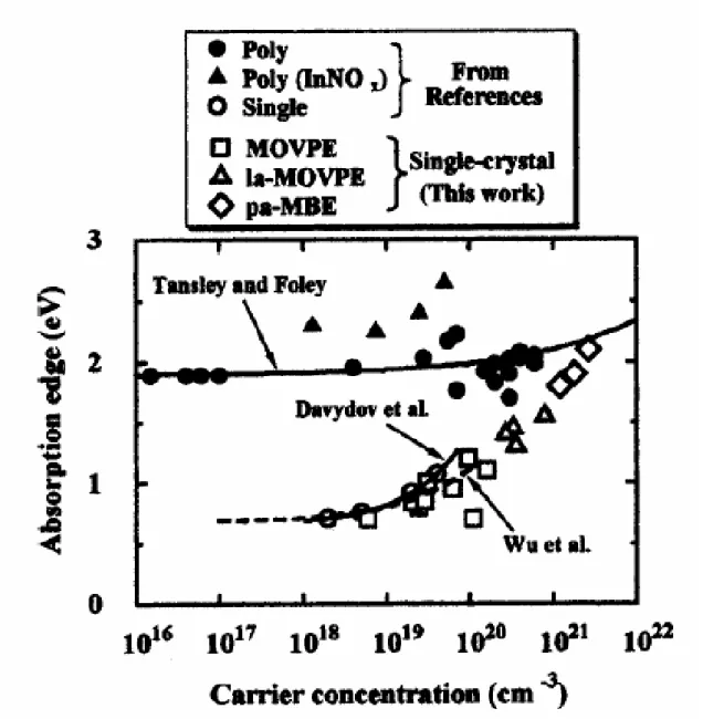
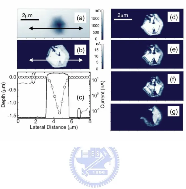
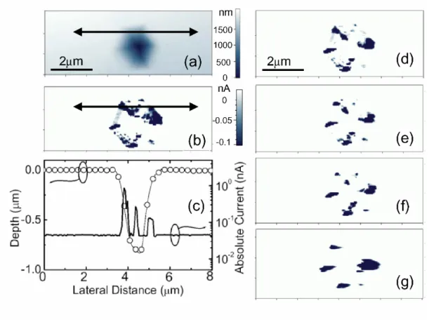
(11) List of Figures. Fig. 1-1. Absorption edge values for InN epilayers grown by different. 9. technology as a function of background carrier concentration. (Ref. 8) Fig. 2-1. A schematic periodic potential (a) and the resulting density of states. 15. (b), a disordered potential (c) and density of states with extended and localized states (d) and with localized states only (e). (Ref. 3) Fig. 2-2. Schematic diagram of densty of states for the extended and localized. 16. states in semiconductor Fig. 3-1. SEM images for (a) sample A without Si-MDLs, (b) sample B with 10. 25. cycles of Si-MDLs, and (c) sample C with 40 cycles of Si-MDLs after H3PO4 etching. Fig. 3-2. Temperature-dependent electron mobility for sample A, B, and C. Dot. 26. and solid curves represent simulation without and with considering short-range potentials. Fig. 3-3. Experimental and simulation (without considering short-range. 27. component) of temperature-dependent mobility for sample A, B, and C. Fig. 3-4. Experimental and simulation considering short-range component of. 28. temperature-dependent mobility for sample C while assume dislocation density at 1×108 cm-3. Fig. 3-5. DLTS spectra for sample A, B, and C. 29. Fig. 4-1. Simultaneous (a) topographic, (b) forward current mapping at +3 V. 39. and 0.2 Hz scan rate. (c) Dual cross-section profile of relative morphologic depth in µm (circle) and local current in nA (line) of GaN V-defect. Current mapping results (d)(e)(f)(g) at scan rates of 1.0, 2.5, 5.0 and 10.0 Hz, respectively. Fig. 4-2. Simultaneous (a) topographic, (b) forward current mapping at -4 V and 0.2 Hz scan rate. (c) Dual cross-section profile of relative morphologic depth in µm (circle) and local absolute value of current in nA (line) of GaN V-defect. Current mapping results (d)(e)(f)(g) at scan rates of 1.0, 2.5, 5.0 and 10.0 Hz, respectively.. IX. 40.
(12) Fig. 4-3. Current-voltage curves (a) and F-N plot (b) at flat region (■),. 41. perimeters (●), off-axis sidewalls (▼), and crest lines (.) of V-defect. (c) Corresponding energy band diagram at equilibrium (dash) and beyond turn-on voltage (solid) of Pt/GaxOy/GaN junction Fig. 4-4. The O(KL1) depth profile of Auger spectra at flat region (solid. 42. square) and inside V-defect (open circle). Inset figure shows the energy survey spectra before ion etching. Fig. 5-1. The gas flow sequences of the FME mode by varying background. 54. NH3 flows Fig. 5-2. The gas flow sequences of the FME mode by varying NH3 flows in. 55. N-step Fig. 5-3. Photoluminescence spectra at 13K and corresponding peak energies,. 56. linewidth, and integrated intensity for InN dots grown by varying background NH3 flow rate. Fig. 5-4. Morphology images for InN dots grown at NH3 flow during N-step of. 57. (a) 0, (b) 500, (c) 1000, (d) 1500, (e) 2000, (f) 3500, (g) 5000, (h) 7000, and (i) 9000 sccm. Inset figures at (a) and (g) represent the magnified images of droplet and InN dots. Fig. 5-5. X-ray diffraction spectra for InN dots grown by various NH3 flow rate. 58. during N-step. Fig. 5-6. Photoluminescence spectra at 13K for InN dots grown by varying. 59. NH3 flow rate at N-step. Inset firgues shows the corresponding peak energies, linewidth, and integrated intensity of PL spectra. Fig. 5-7. Equivalent thickness and amount for In droplets and InN dots,. 60. respectively as a function of NH3 flow rate during N-step. Fig. 6-1. The gas flow sequences of the growth interruptions mode.. 71. Fig. 6-2. Images of SEM for interruptions time at (a) 0, (b) 5, (c) 10, (d) 15, (e). 72. 20, and (f) 40 seconds per cycle. Fig. 6-3. SEM images of the (a) In droplet, (b) small InN dot for 0 second. 73. interruptions, and (c) large InN dot for 15 seconds interruptions. Fig. 6-4. The total amount and separated values of In for droplet, small and large dots as a function of interruption times. The inset figure shows the intensity ratio of x-ray diffraction at (101)-In over (0002)-InN. X. 74.
(13) Fig. 6-5. 13K photoluminescence spectra for InN grown at various interruption. 75. times. The inset schematically shows recombination mechanism of degenerate electrons to the bandtail and deep level state. Fig. 6-6. SEM images for the 0s-sample before (upper) and .after (down) HCl. 76. etching. Fig. 6-7. X-ray diffraction spectra before and after HCl etching (symbol in. 77. solid and dotted curves, respectively) for InN samples with various interruption-step time. Fig. 6-8. Time-resolved PL spectra at various energies for interruption-step time of (a) 10 and (b) 15s. (c) and (d) reveal the corresponding decay time as a function of energy and time-integrated PL intensity spectra in dash lines. Solid lines indicate the fitting curve for the equation Eq. (2.5).. XI. 78.
(14) Chapter 1 Introductions 1.1 Electrical properties of group III-nitrides epilayer and microstructures Group III-nitrides materials, such as AlN, GaN, InN and its alloys have recently become fundamentally important for optoelectronics, including in bright light emission diodes (LED), laser diodes (LD) and photodetectors, because of the direct bandgap feature and the coverage of the ultraviolet to the infrared regions. However, the development of group III-nitrides will continue to be negatively affected by the lack of lattice-matched substrates. As for the most commonly used (0001)-Al2O3 substrate, point defects and structural defects, such as threading dislocations, inversion domains (IDs), V-shaped defects (V-defects) and hillocks, are normally observed in the nitride epilayers. Native point defects typically act as nonradiative recombination centers which reduce luminance efficiency and increase leakage current, affecting device performance. Threading dislocations with a density of 109 to 1011 cm-2 are separated into three groups: edge, mixed and screw. These native defects can degrade both electrical and optical properties, such as by reducing electron mobility via scattering from charged edge-type threading dislocations1) or reducing photoluminescence intensity via non-radiative recombination2).. Deep-level transient spectroscopy (DLTS) and photoluminescence (PL) used to be effective tools for probing the density and corresponding energy levels inside the. 1.
(15) forbidden gap associated with point defects. Nevertheless, within the limits of spatial resolution, typically around several hundreds of micrometers, fundamental knowledge of sub-micrometer single structural defects is still lacking.. Peculiar electrical and optical properties around these defects, especially V-defects and hillocks, have recently been elucidate based on such microscopic characterization. techniques,. as. cathodoluminescence. (CL),. microscopic. photoluminescence (μ-PL), scanning tunneling microscopy (STM), and near-field scanning optical microscopy (NSOM). The early literature showed that V-defects in InGaN/GaN multiple quantum wells may be connected to threading dislocations, stacking faults or inversion domains. The formation of V-defects further enhanced indium segregation, such that localization excitonic recombination produced a long-wavelength shoulder in luminescence spectra3). Our group had demonstrated that the Al0.16Ga0.84N epilayer yields an extra peak at 350 nm from the center of the V-defects and with a significantly stronger intensity than the near-band-edge emission at 335 nm4). The 350 nm emission band is attributed to shallow acceptor levels, probably associated with VGa defects. Besides, strong emission at 351 nm was observed from hillocks in Al0.11Ga0.89N films5). The temperature-dependent µ-PL measurement demonstrates a S-shaped behavior with a transition temperature of ~120 K, which is lower than that of typical near-band emission, suggesting that the Al content in the hillocks is lower than that in the surrounding area. As well as the particular optical properties, the electronic properties of the structural defects are also of interest. E.G. Brazel et al.6) and J. W. P. Hsu et al.7) directly observed enhanced. 2.
(16) current density in small localized areas around dislocations and hillocks. The increase in conductivity around the microstructures provides a great advantage on light emission diode, because the spreading of electrons into active layer is enhanced. However, the conduction mechanism remains unclear.. Chapter 3 investigates the electrical properties of the GaN with various dislocation densities. A large increase in electron mobility at room temperature from 57 to 300 cm2/V-s, and a drop in the etching pit density from 108 to 7×106 cm-2 are observed. The simulation of temperature-dependent electron mobilities demonstrated that, as well as the traditionally accepted lattice phonon and long-term Columbic ionized impurities, long-range charged threading dislocations and short-range point defects limit the electron transport in GaN with dense and sparse dislocations, respectively. Chapter 4 describes electrical studies of GaN V-defects by conductive atomic force microscopy. The forward current conductivity in the V-defect region is much higher than in the surrounding area. However, a snowflake-like current pattern is observed when the sample is negatively biased. Further static current-voltage measurements suggest that Schottky emission and Fowler-Nordheim tunneling determines the carrier transport in the V-defect region and surrounding area, respectively.. 3.
(17) 1.2 Current status of fundamental optical properties of InN During the last few years, interest in InN has been remarkable, because of many properties that are exhibited by all group III-nitrides. InN has the lowest effective electron mass and therefore a high mobility and high saturation velocity. The theoretical maximum electron mobility and drift velocity of InN at room temperature are approximately 4400 and 4.2×107 cm/s, respectively, indicating that the InN-based field-effect transistor has great potential with a cutoff frequency of over 1 THz for 100 nm gates.. Since the lattice constant along the a-axis of InN, 3.54 Å, exceeds that of GaN, 3.18 Å, and AlN, 3.11 Å, InN is expected to have the lowest bandgap of the group III-nitrides. However a controversy regarding the exact value continued until only a few years ago. Before 2000, InN fabricated by reactive radio frequency sputtering was generally accepted to exhibit an absorption edge of approximately 1.9 eV at room temperature. However, InN films grown by molecule beam epitaxy (MBE) and metalorganic chemical vapor deposition (MOCVD) since 2000 has been revised sharply down to a lowest value of about 0.7 eV8), as plotted in Fig. 1-1. The absorption edge energy is close to theoretically simulated bandgap energy, based on density functional theory (DFT) with the local density approximation (LDA) and quasiparticle theory, which shifts the theoretical ab initio prediction to under 1 eV. Additionally, a large amount of oxygen and excess nitrogen is demonstrated to be incorporated in sputtered InN, producing nonstoichiometric InxNyOz or InxNy and increasing the bandgap energy9). 4.
(18) Several works, which have applied various growth conditions have extensively described the variation in the bandgap of InN between 0.65 and 2 eV. Using MBE technology, H. Lu and W. J. Schaff at Cornell University pioneered the production of an InN epilayer on sapphire using a GaN or AlN buffer layer at 2001. As the thickness is increased from 10 to 7500 nm, the background electron concentration decreases gradually from 5×10¹⁹ to 4×1017 cm-3 , as determined by Hall measurement at 300 K10). This value is lower than the density of states in the conduction band, so a non-degenerate InN epilayer is produced. The absorption edge at 300 K of the least concentrated sample is around 0.67 eV. A rapid increase in the absorption edge as the electron concentration increases above 1018 cm-3 is observed, reaching about 1.5 eV at approximately 1020 cm-3. The so-called Burstein-Moss shift of the absorption edge with the electron concentration has been determined to be consistent with the increase in the Fermi level as the lowest conduction band is filled with electrons. The dependence can be well described by assuming the existence of a non-parabolic conduction band due to the k.p interaction between the conduction band and the valence bands, in which the effective mass of the electron also depends on carrier concentration11). This fact is consistent with the photoluminescence, in which an emission band peaks at 0.675 eV with a linewidth of less than 20 meV at low temperature, revealing a non-degenerate InN epilayer12). V. Cimalla et al. identified the origin of the thickness-dependent concentration of electrons in for MBE-grown InN epilayers10). Surface accumulation, which is commonly attributed to the low Branch point or surface oxygen contamination, critically influences InN layers that are thinner than 300 nm. When the InN thickness is around several micrometers, the 5.
(19) density of dislocations is the major determinant background doping. Finally, point defects, such as vacancies and impurities, have a weak influence and dominate the free electron concentration, only at InN >10 μm.. Methods for growing InN using an MBE system had been advanced. Epilayers or microcrystals13) that is larger than several hundreds of nanometers have been demonstrated to have exceptional optical properties with a low-temperature peak energy less than 0.68 eV and a linewidth of less than 20 meV. Several groups believed that growth under slightly In-rich conditions byMBE improves quality. However, the growth of InN using MOCVD is much more complex and faces many challenges. Section 1.3 discusses important parameters for optimizing InN grown by MOCVD.. 6.
(20) 1.3 Important issues in growth of InN by MOCVD Fewer investigations have been published on the optical properties of MOCVD-grown InN than on the growth of InN films by MBE. Recently, A. Yamamoto reported a carrier concentration of the order of 1018 cm–3 for InN films grown by atmosphere- pressure MOCVD at approximately 600℃14). The growth temperature is clearly around 100℃ higher than that by MBE because NH3 acts as a group-V precursor, which requires a higher pyrolyzing temperature. Accordingly, a high flow rate of NH3 is required to prevent droplet formation, in which the V/III molar flow ratio from exceeding 104. However, a high V/III ratio results in the decomposition of a large amount of NH3 to form hydrogen, followed by a drop in growth rate15) and photoluminescence intensity quenching16). Another challenge is that InN begins to decompose as the temperature exceeds 630℃, so In droplets cover the surface, with a growth rate of InN that decreases by an order of magnitude as the growth temperature increases from 600 to 700℃17). In summary, conventional MOVPE growth can proceed within a narrow range of growth temperature and flow rate.. Chapter 5 introduces a modified growth mode called flow-rate modulation epitaxy (FME) for InN nanostructures grown at 600℃. This technique is characterized by repetitive cycles of alternately supplied indium and nitrogen precursors. Tuning a low background NH3 flow during the supply of In improves the optical properties beyond those obtained by growth in the conventional mode. In addition, the degradation effects on both growth rate and luminescence efficiency are 7.
(21) eliminated even for a high V/III ratio.. Chapter 6 demonstrates the use of repetitive growth interruptions for fabricating InN at high temperature. At 700℃, liquid In is converted to solid InN when the interruption time exceeds 15s per cycle. Low-temperature photoluminescence spectra show emissions at 0.70 eV for droplet-free samples. The dependence of the PL decay times on emission energy indicates that the localization of photogenerated holes is important in the recombination at about 0.70 eV of the long-interrupted samples.. 8.
(22) Fig. 1-1 Absorption edge values for InN epilayers grown by different technology as a function of background carrier concentration. (Ref. 8). 9.
(23) Chapter 2 Theoretical background 2.1 Brief deposition. overview. of metalorganic chemical vapor. Although the development of a comprehensive growth model for metalorganic chemical vapor deposition (MOCVD) is highly complex, G. B. Stringfellow18) subdivided the fundamental processes into thermodynamic and kinetic components. Briefly, thermodynamics determine the driving force of the overall growth process, in which mass transport controls the rate of transport of the material to the growing interface, and kinetics process controls the rates of chemical reactions that occur either homogeneously in the gas phase or in a heterogeneous process depending on the surface structure.. The growth rate, as macroscopic quantity, depends on external parameters, such as temperature and input precursors flow rates. Growth rate generally increases with temperature, characteristic of a process limited by chemical reaction kinetics. In the homogeneous process, the rate constant ofa chemical reactions is expressed as. kAB = (kT/h)K*AB.. (2.1). K*AB, the equilibrium constant of the reaction, can be written in terms of the free energy of activation. Table 2.119) lists the equilibrium constants for group III-nitrides. The thermal decomposition rates of group-III and group-V precursors should be 10.
(24) considered. The pyrolyzing efficiency of NH3 is much lower than that of group-III precursors, such as trimethylgalium (TMGa) and trimethylindium (TMIn), because of the stronger N-H bond, and so is the limiting factor of the kinetics of the growth of group-III nitride.. Table 2.1 Equilibrium constants for group-III nitride reactions Reactions. Log10[K*AB(K)]. Ga(g) + NH3(g) = GaN(s) + (3/2)H2(g). 12.2 +1.78×10⁴/T +1.79log10(T). In(g) + NH3(g) = InN(s) + (3/2)H2(g). 13.1 +1.13×10⁴/T +2.29log10(T). Al(g) + NH3(g) = AlN(s) + (3/2)H2(g). 14.2 +3.17×10⁴/T +2.33log10(T). At relatively high temperatures, the chemical reactions are very rapid since they depend exponentially on temperature. The growth rate is not controlled by the chemical reaction but rather by the rate at which the minority species are transported through the vapor phase to the interface.. In this regime, the growth rate is independent of the temperature. It is generally called the mass-transport-limited regime. The growth rate is mainly limited by mass transport, and the flux depends linearly on the difference between the partial pressure at vapor phase and at growth interface and is expressed as,. J=(D/RTδ)×(p*-pi),. (2.2). where D is the diffusion coefficient in vapor phase; p* is the input partial pressure; pi is the partial pressure at the solid/vapor interface, and δ is the thickness of the. 11.
(25) boundary layer. Moreover, further increasing the temperature results in abnormal behavior that reduces the growth rate by various complex processes, such as decomposition or evaporation from the solid phase, and parasitic reactions.. 12.
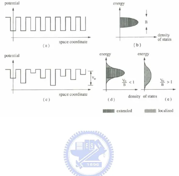
(26) 2.2 Localization of photoluminescence Photoluminescence is a powerful and non-destructive tool for measuring the optical properties of a semiconductor. Electron-hole pairs are generated by an overbandgap excitation, via quasi-thermal equilibrium distribution, and then radiative recombination occurs and photons are released. The peak energy of the PL spectrum of the direct bandgap semiconductor fundamentally reveals the band gap energy. However, impurities and defects cause electron-hole pairs to recombine radiatively via the energy level inside the forbidden gap or to recombine by absorption via non-radiative recombination.. A relationship between the bandgap energy and the temperature of the semiconductor is proposed based on Varshini’s experimental finding,. EG(T) = E0 – αT2/(β +T),. (2.3). where E0 is the bandgap energy at 0 K, and α and β are Varshini’s fitting parameters. When a deep level, such as an impurity levels or a quantum confinement level, is present in the forbidden bandgap, the localization of photogenerated electrons or holes may affect the PL spectrum20) and cause a discrepancy from Varshini’s description. Figures 2-1(a) and (b) schematically depict a periodic Kronig-Penney potential and its corresponding density of states, for a particular width B. When the potential is disturbed, as plotted in Fig, 2-2(c), that the depth of the potentials varies in a width V0, the sharp edges of the density of states become smeared out with additional exponential tails in Fig. 2-2(d). E. Cohen and M. D. Sturge21) solved the Schrödinger 13.
(27) equation for random perturbations of potential in real space and obtained a exponential-form bandtail When localized holes gain energy, they more easily escape from the bandtail, in which the density of states is proportional to the transfer probability.. For a semiconductor system, potential fluctuations cause localization with a tailing parameter E0, which specifiesthe density of states in the exponential tail as. D(E) = (N0/E0)exp(-E/E0),. (2.4). where N0 is the total number of tail states. When E0 is much lower than EG, the density of localization states that is related to the extended states are as shown schematically in Fig. 2-2. At higher energy, excitons lie in extended states, making their transfer from higher energy sites to lower energy sites easier than by direct recombination. The lifetime of excitons is determined by the rate of transfer. At lower energy, one carrier whose Bohr radius is smaller than the width of the potential in real space is localized, and another is bound to it by Coulombic attraction, and a slower radiative recombination governs the lifetime of the excitons. The transition energy between localized and extended states is called the mobility edge Eme, in which the recombination rate equals the rate of transfer. Accordingly, the lifetime of excitons, considering the localization, is expressed as. τ(E) = τrad / {1+exp[(E-Eme)/E0)]},. (2.5). where τrad is the radiative lifetime of direct recombination. 14.
(28) Fig. 2-1 A schematic periodic potential (a) and the resulting density of states (b), a disordered potential (c) and density of states with extended and localized states (d) and with localized states only (e). (Ref. 3). 15.
(29) Fig.2-2 Schematic diagram of densty of states for the extended and localized states in semiconductor.. 16.
(30) Chapter 3 Carrier scattering in GaN films with low dislocation density. When nitride-based thin films are used in optoelectronic devices, threading dislocation density is a factor that critically affects commercializability. One of the important related issues is that electronic states associated with core dislocations constitite scattering centers and reduce mobility1). Approximately 1010 cm-2 of charged dislocations dominate the scattering process and are responsible for extremely low mobility and the T3/2-dependence22). The temperature-dependence of mobility at low dislocation density involves both positive and negative powers of temperature. However the simulated mobility, considering lattice vibration, ionized impurities and charged dislocation scattering, diverges from the experimental results23,24).. This chapter presents variable-temperature Hall measurements for undoped GaN films with various etching pit densities (EPD) using Si-modulation doping interlayers(Si-MDLs). Point defects are suggested as another source of scattering and, resulting in good fitting at the low dislocation density epilayer. Deep-level transient spectroscopy (DLTS) results further indicate that nitrogen interstitials behave as reasonable scattering centers.. 17.
(31) 3.1 Experiment details. The GaN films employed herein were grown on (0001)-sapphire substrates at a temperature of 1100 ℃ using a low-pressure horizontal metalorganic chemical vapor deposition (MOCVD) reactor. Trimethylgallium (TMGa) and ammonia (NH3) were used as Ga and N source precursors in the deposition.. Three undoped GaN films labeled A, B and C were grown with slightly Si-modulation doping layers (Si-MDLs). After 0.6 μm undoped GaN film was deposited on sapphire, 0, 10, and 40 periods of MDL was sequentially grown and capped of 1.2 μm-thick undoped GaN. The basic unit of MDL is a pair of Si-doped and undoped GaN layers, both with a thickness of 7.5 nm. The flow rate of Si-doping layers is 8.8×10⁻¹⁰ mol/min. To determine the dislocation density, EPD was obtained by counting the hexagonal pits on the surface after immersion in H3PO4 boiled at 220 ℃. for. 15. min,. using. scanning. electronic. microscopy. (SEM). images.. Temperature-dependent Hall measurements were made to investigate the scattering mechanism of a series of GaN films with various EPDs from 77 to 300 K. Additionally, to confirm whether electrically active point defects are present in the bandgap of undoped GaN and to determine their density, deep-level transient spectroscopy (DLTS) measurements were made on Schottky diodes in these samples using HP4194A in a temperature range from 370 to 200K.. 18.
(32) 3.2 Temperature-dependent scattering of electrons in GaN. Figure 3-1 presents SEM images of samples A, B and C after etching in H3PO4. Each of the etched pits was further verified to have a well-defined hexagonal shape and a singly sloped sidewall, like the so-called “α type” etched pit identified by T. Hino et al., who claimed that such etched pits terminate screw-type threading dislocations that were observed on cross-sectional transmission electron microscopy (TEM) images25). The etching pit densities of samples A to C are 5.6×10⁸, 3.1×10⁷ and 7.1×106 cm-2, respectively. Together with a drop in EPD, an increase in electron mobility at room temperature from 57 to 322 cm2/Vs reveals that Si-MDLs yields GaN epilayer of higher quality.. Figure 3-2 plots the electron mobility in samples A to C as a function of temperature, obtained by temperature-dependent Hall measurement. Samples B and C have a lower EPD and transport coefficients that depended on both positive and negative powers of temperature. However, in sample A, with an EPD of over 5×108 cm-2,. the. temperature-dependent. transportation. exhibits. only. a. positive. power-dependence of temperature. Phonon scattering and ionized impurity scattering were initially considered to explain the experiment results. An extremely high density of ionized impurities in sample A may have increased the probability of collision between electrons and impurities rather than phonons, causing the mobility to exhibit a positive power-dependence on temperature. However, the carrier concentrations in these three samples all are in the range 5~10×1016 cm-3, introducing another scattering. 19.
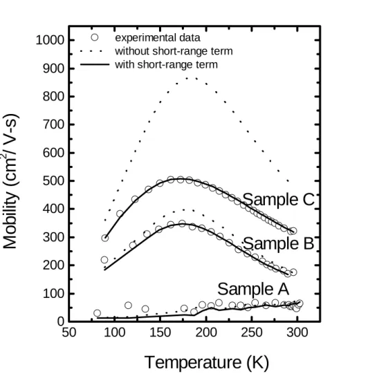
(33) mechanism.. Based on theoretical calculations, charged dislocation lines are speculated to apply long-range Columbic forces on laterally moving electrons, affecting the temperature-dependent mobility1,22-23). Calculation of the momentum relaxation rate due to the screening potential of the dislocations and averaging over energy yields the mobility due to dislocation scattering as. μ Dis. h 3ε S c 2 (1 + 4λ2 k 2 ) 3 / 2 = N Dis (m*) 2 e 3 λ4 2. (3.1). where λ is the Debye screening length; k represents the perpendicular wave vector, and NDis as the density of edge-type dislocations from 1×10⁸ to 7.5×109 cm-2. Dislocation scattering combined with Matthiessen’s rule with phonon and ionized impurity-scattering26) yields the simulated (dotted) curves in Fig. 3-3. For sample A with the lowest mobility, the simulated curve is well fitted with a dislocation density of 7.5×109 cm-2. The experimental dislocation density is about an order of magnitude higher than that obtained by EPD. Based on theoretical calculations and the results of scanning Kelvin probe microscopy (SKM), only dislocations with an edge component were associated with a negatively charged electronic state27). The density of screw-type dislocations, determined by EPD given according to K. Shijima, is an order of magnitude lower than that of edge-type dislocations28). Figure 3-3 also shows that samples B and C require a low density of charged dislocations, and the corresponding simulated curves are discrepant at temperatures of over 150 K. The more rapidly drop in electron mobility as temperature increases implies the existence 20.
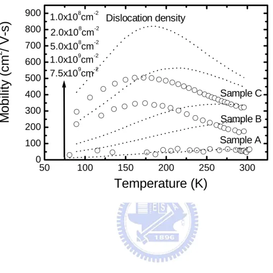
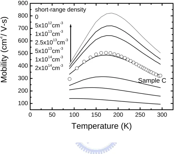
(34) of another scattering mechanism with a negative power-dependence on temperature.. D. C. Look and Q. S. Zhu claimed that short-range scattering centers, such as space charges or defects form a square-wall potential of radius r0 and potential depth U024,26). A quantum-mechanical calculation for the cross-section based on the square-well scattering potential yields the mobility, which is related to short-range scattering as. μ short =. h 4e 1 (k BT ) −1/ 2 2 6 5/ 2 16π 3 (m*) N shortU 0 r0 9. (3.2). where Nshort denotes the short-range scattering center density. Basically, as the temperature increases, electron acceleration leaves from long-range scattering region, but the probability of collision is increased by the presence of more short-range scattering centers. Figure 3-4 plots simulated curves and experimental results (as circles) for sample C with dislocation density 1×108 cm-2 and various densities of short-range scattering centers in the range from 7×10¹³ to 1×1014 cm-3. The figure indicates that dislocation scattering dominates mobility at low temperature, even at a density of less than 1×108 cm-2. At higher temperature, scattering from the short-range potential with a density of approximately 2.5×1013 cm-3 is more important than scattering from dislocations. Finally, substituting Eqs. (3.1) and (3.2) into traditional Matthiessen’s rule yields the estimated values in Table 3.1.. 21.
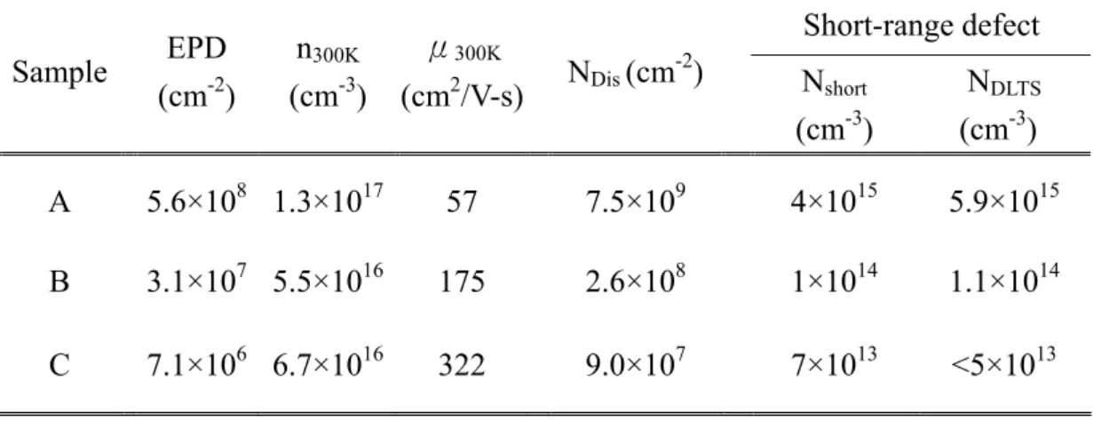
(35) Table 3.1. The experimental results of etching pits density, room-temperature Hall measurement, and deep level transient spectroscopy. NDis and Nshort are estimated values from temperature-dependent mobility.. Sample. EPD (cm-2). n300K (cm-3). Short-range defect. μ300K. -2. (cm2/V-s). NDis (cm ). Nshort (cm-3). NDLTS (cm-3). A. 5.6×10⁸ 1.3×10¹⁷. 57. 7.5×10⁹. 4×10¹⁵. 5.9×10¹⁵. B. 3.1×10⁷ 5.5×10¹⁶. 175. 2.6×10⁸. 1×10¹⁴. 1.1×10¹⁴. C. 7.1×10⁶ 6.7×10¹⁶. 322. 9.0×10⁷. 7×10¹³. <5×10¹³. 22.
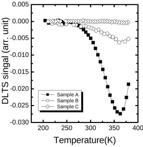
(36) 3.3 Deep level in undoped GaN epilayer. To identify the origin of short-range scattering centers, DLTS with a bias of -1V and an emission rate window of 0.125 s-1 was applied with periodic pulsing to 0 V for trap filling). In Fig. 3-5, in the temperature range from 380 to 200K, one deep level peaks at 360 K in samples A and B, while in sample C, the singal is below the detection limit. Based on the peak intensity, trap densities of the three samples of 5.9×10¹⁵, 1.1×10¹⁴ and under 5×1013 cm-3 are obtained.. According to the principle. of detailed balance, the derived energy level associated with the prominent peak are at EC-1.01±0.09 eV. Like the Arrhenius plot29), this level is consistent with the so-called E4 level, which is thought to be associated with nitrogen interstitials.. As indicated in Table 3.1, the estimated value of Nshort is consistent with the density of the deep level, determined using DLTS, NDLTS. In addition, the effective range of capture by nitrogen interstitials is only several Angstroms, indicating that they are candidate short-range scattering centers.. 23.
(37) 3.3 Summary. In summary, Si-modulation doped layers were introduced to improve the quality of GaN epilayers. After 40 cycles of MDLs, the etching pits density is reduced from 5.6×10⁸ to 6.5×106 cm-2, indicating that the density of threading dislocations is reduced. In low-dislocation samples, an increase in the room-temperature mobility from 57 to 322 cm2/V-s is also demonstrated. To interpret the variation in the transport behavior. of. GaN. epilayers. with. the. density. of. threading. dislocations,. temperature-dependent mobility was measured and fitted reference to various scattering mechanisms. At high dislocation density, low mobility may be dominated by Columbic interaction with charged dislocations. As the dislocation density decreases, free electrons at high temperature interact with charged dislocations with increasing difficulty, while they more easily collide with point defects as short-range scattering centers. According to the consistency between the estimated and the results obtained by DLTS, the short-range scattering centers may be nitrogen interstitials with an energy level of EC-1.01±0.09 eV.. 24.
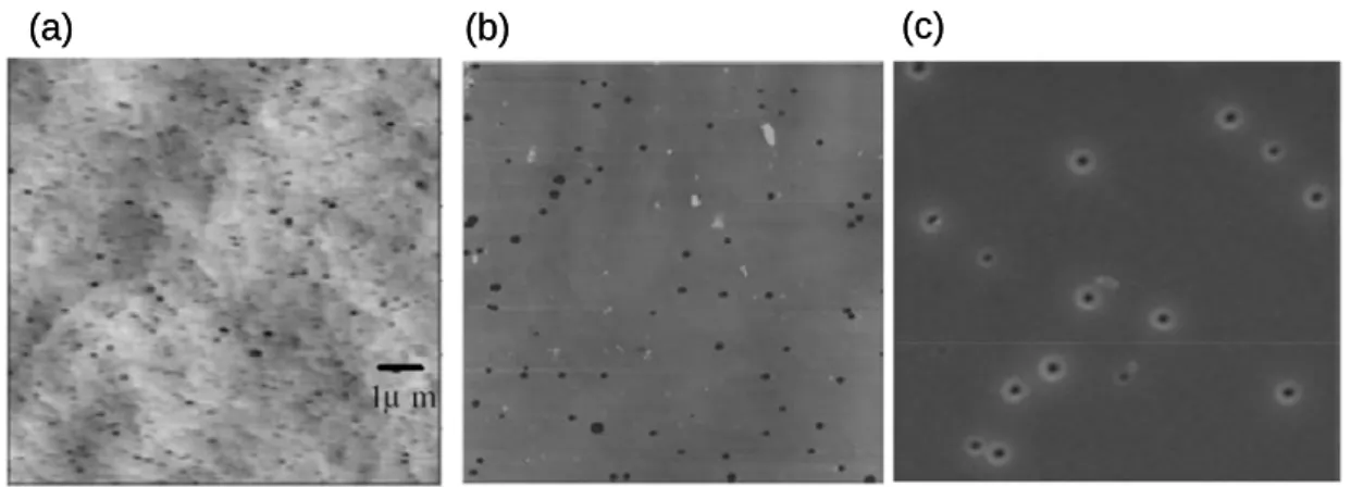
(38) (a). (c). (b). Fig. 3-1 SEM images for (a) sample A without Si-MDLs, (b) sample B with 10 cycles of Si-MDLs, and (c) sample C with 40 cycles of Si-MDLs after H3PO4 etching.. 25.
(39) 1000 900. experimental data without short-range term with short-range term. 2. Mobility (cm / V-s). 800 700 600 500. Sample C. 400 300. Sample B. 200. Sample A. 100 0 50. 100. 150. 200. 250. 300. Temperature (K). Fig. 3-2 Temperature-dependent electron mobility for sample A, B, and C. Dot and solid curves represent simulation without and with considering short-range potentials.. 26.
(40) 2. Mobility (cm / V-s). 900 1.0x108cm-2 Dislocation density 8 -2 800 2.0x10 cm 700 5.0x108cm-2 9 -2 600 1.0x10 cm 9 -2 500 7.5x10 cm. Sample C. 400 300. Sample B. 200. Sample A. 100 0 50. 100. 150. 200. 250. 300. Temperature (K). Fig. 3-3 Experimental and simulation (without considering short-range) of temperature-dependent mobility for sample A, B, and C.. 27.
(41) 2. Mobility (cm / V-s). 900 short-range density 0 12 -3 5x10 cm 13 -3 1x10 cm 13 -3 2.5x10 cm 13 -3 5x10 cm 14 -3 1x10 cm 14 -3 2x10 cm. 800 700 600 500 400 300. Sample C. 200 100 0. 50. 100. 150. 200. 250. 300. Temperature (K). Fig. 3-4 Experimental and simulation considering short-range component of temperature-dependent mobility for sample C while assume dislocation density at 1×108 cm-3.. 28.
(42) DLTS singal (arr. unit). 0.005 0.000. -0.005 -0.010 -0.015 -0.020 Sample A Sample B Sample C. -0.025 -0.030. 200. 250. 300. 350. Temperature(K). Fig. 3-5 DLTS spectra for sample A, B, and C.. 29. 400.
(43) Chapter 4 Current properties of GaN V-defects. In recent years, remarkable progress has been made in the development of nitride-based optoelectronic and electronic devices, including high-brightness devices, blue-green light-emitting diodes (LED), violet laser diodes (LD) and high-power microwave devices. However, the lack of a lattice-matched substrate can lead a high density of threading dislocations, hillocks, nanopipes and particularly surface V-defects in epitaxially grown nitride film. The appearances of these native defects can give rise to anomalous behaviors associated with the the electrical and optical properties of the film. E.G. Brazel et al.6) directly observed high current densities and low effective Schottky barrier heights in small localized areas around dislocations. J. W. P. Hsu et al.7) and J. Spradlin et al.30) further reported on the increase in current conduction at hexagonal GaN hillocks. Several groups31,32) had shown that In-riched dots are formed on the apexes of InGaN/GaN multiple quantum well-associated V-defects, accompanied by the formation of thinner quantum wells on the inclined facet region. A. A. Pomarico et al. observed enhanced current conduction mainly at the perimeters of V-defects on an n-type GaN sample under forward bias using conductive atomic force microscopy.. This work includes electrical studies of GaN V-defects and observes a different distribution pattern of current conduction. The results show that the forward current. 30.
(44) conductivity in the V-defect region is much higher than in the surrounding area. A snowflake-like current pattern is observed when the sample was biased negatively.. 31.
(45) 4.1 Experimental details The sample used in the microscopic analysis was grown on a conducting 6H-SiC substrate, which was supplied by Epistar Co. Ltd. The film comprises a 150 nm-thick Al0.13Ga0.87N buffer layer that is grown at 1000 ℃ and a 2.3 μm-thick Si-doped GaN layer at 1050 ℃ with a carrier concentration of 6.5×1017 cm-3. The measured surface V-defect density is about 105 cm-2, with a diameter that varied from the typical value of 1.4 to 2.7 µm.. An NT-MDT Solver HV atomic force microscopy system was utilized to make conductive AFM measurements. The contact mode was applied to profile the surface topography and allow the concurrent C-AFM measurement of to map the localized current distribution and to extract a static current-voltage relationship. The AFM tip acts as a nanometer-sized Schottky contact on the GaN sample with a current from 50 pA to 30 nA.. 32.
(46) 4.2 Current mapping Figures 4-1(a) and (b) plot the simultaneous measurement of surface morphology and the current response, respectively, of a single V-defect, biased at +3 V, with a scan rate of 0.2 Hz . The brighter regions are higher and have larger forward current. Under this experimental condition, the forward current is detected across the entire V-defect region with a saturated value as high as ~27 nA - about three orders of magnitude higher than that measured outside the V-defect region, 40 pA. Notably, the results herein differ significantly from those of A. A. Pomarico et al.32) whose current was measurable only at the perimeters of the V-defect under forward bias. The C-AFM measurements are also very sensitive to the scan rate. Figures 4-1(b), (d), (e), (f) and (g) present the C-AFM current profiles obtained at scan rates of 0.2, 1.0, 2.5, 5.0 and 10.0 Hz, respectively. As the scan rate is increased, the grey and darker regions in the C-AFM image begin to be visible inside the V-defect, starting at the upper and lower off-axis facets, and eventually evading most of the central region of the V-defect at the highest scan rate of 10.0 Hz. Indeed, at the highest scan rate, the results are not far from those of Pomarico, described above. From the above discussion, when the surface conductivity of the microstructures is profiled, the scan rate should be considered since a higher scan rate seems inevitably to result in poorer electrical contact between the tip and the sample in C-AFM.. Figure 4-2 displays the surface morphology and current images of the V-defect biased at -4 V and measured at various scan rates. Here, darker regions in AFM and C-AFM images represent greater depth and higher reverse current, respectively. As 33.
(47) expected, the use of a low scan rate is critical to uncovering accurate leakage current distributions. As the scan rate is decreased from 10 Hz (Fig. 4-2 (g)), the current leakage area begins to extend from the outermost corners toward the V-defect center along the crest lines, and around the perimeters of the V-defect. A snowflake-like leakage current pattern is observed in the V-defect at a scan rate of 0.2 Hz (Fig. 4-2 (b)). Additionally, not all of the aforementioned parts of the sample exhibit current leakage of the same magnitude. The current leakages on the crest lines, the perimeters and the other regions are approximately 1, 0.1 and 0.05 nA, respectively, in the GaN V-defect - nearly 20 times the current.. 34.
(48) 4.3 Static current-voltage characterizations To investigate the microscopic electrical properties of GaN V-defects, static current-voltage measurements of the samples were made. Figure 4-3(a) plots the local current-voltage curves along the crest lines, perimeters, off-axis sidewalls and around the flat region of a V-defect that is shown in Fig. 4-2. The static forward I-V characteristics of Fig. 4-3 includes turn-on voltages, an abrupt increase of current, and crest lines , perimeters and off-axis facets at 0.49, 0.63, and 0.81V, respectively. These values are markedly lower than that measured in the flat region, 3.26 V, causing the V-defects to act as effective current leakage paths in the GaN/SiC film.. Based on the reverse static I-V characteristics, current breakdown occurs first at the crest lines, and then at the perimeters of the V-defect. The corresponding breakdown voltages are -2.5 and -3.9 V, respectively. However, no breakdown phenomenon is observed up to -9 V on either the off-axis facet or the flat region. The static I-V results show the lower breakdown voltages on both crest lines and perimeters than elsewhere are the primary cause of the snowflake current pattern in the C-AFM image under a reverse applied bias.. The forward current that flows through GaN from the AFM tip in the flat region exhibit essentially the Fowler-Nordheim tunneling effect33), as revealed by the linearity of the log I/V2 vs. 1/V curve in the F-N plot (squares in Fig. 4-3 (b))34) and the turn-on voltage at 3.26 V (Fig. 4-3(a)). The presence of an F-N current indicates the presence of an ultra-thin dielectric layer between metal tip and surface, most likely. 35.
(49) the native oxide GaxOy, which is an additional energy barrier to against the flow of carriers between the underlying GaN film and the metal tip. Figure 4-3(c) presents the Pt/GaxOy/GaN band diagrams at equilibrium and at a an applied bias that exceeds the turn-on voltage, where φM is the work function of metal Pt (5.6 eV), and χox and. χ GaN are the electron affinities of GaxOy (2.5±0.2 eV)35) and GaN (4.1 eV), respectively. At a low forward bias, a negligible current flows in the device, as presented in Fig. 4-3(a); it is believed to be associated mainly with traps or direct tunneling35). However, as the applied voltage is increased beyond the turn-on voltage, ( φM- χox)/e, the potential barrier begins to transform from trapezoid to triangular (Fig. 4-3(c)), and the F-N tunneling begins to overwhelm the carrier transport, sharply increasing the forward current by continuously reducing the thickness of the effective barrier. The measured turn-on voltage of 3.26 V appears to be very close to the predicted value, 3.1±0.2 V. This consistency between the theoretical and experimental values further verifies the F-N tunneling in the flat region.. Following from the above discussion of forward I-V characteristics in the V-defect region, the F-N tunneling may govern the forward carrier transport in the V-defect region, because of the similar linear-like relationship between log(I/V2) and 1/V (circles, upward and downward-pointing triangles in Fig. 4-3(b)). However, the turn-on voltages of the sharply increasing current, whether at the crest lines, the perimeters or the off-axis facets (0.49, 0.63, and 0.81 V), are much lower than the predicted value (3.1±0.2 eV), and are not completely characteristic of F-N tunneling. Fundamentally, three major current mechanisms apply; they are F-N tunneling, direct. 36.
(50) tunneling and Schottky-like transport, which all contribute to the flow of carriers in a thin MIS structure that is biased at high voltages, which dominate interchangably as the thickness of the insulating layer decreases. Both F-N tunneling and Schottky-like transport are associated with abruptly increasing field emission characteristics, whereas direct tunneling is associated with a smooth voltage-dependent curve36). The sharp rise in the current strongly suggests the carriers flow between the metal tip and GaN in the V-defect region primarily by Schottky-like carrier emission. If so, then a native oxide with a thickness of less than 1 nm will form inside the V-defect region, eliminating its suppression of carrier flow.. The Auger spectroscopic depth profile in Fig. 4-4 reveals that the oxygen concentration drops more in the V-defect than in the flat region. In the flat region, the oxygen O(KL1) signal begins to drop after 4s of ion etching, whereas in the V-defect region, it decreases after only 1s. The native oxide thickness in the flat region is approximately 2-3 nm, suggesting that a native oxide with a thickness of less than < 1 nm is formed in the V-defect region. This fact, in turn, strongly supports the claim that Schottly emission explains the carrier flow between the Pt tip and GaN in the V-defect area. The calculated barrier heights at the crest line, perimeter and off-axis facet are 0.6, 0.71 and 0.82 eV, respectively. They are considerably lower than the predicted value φM- χGaN, 1.5 eV. The origins of the lowering of the barrier height are still under investigation. We suggest that a partial explanation lies in the formation of excess surface states37) in the GaN V-defect region.. 37.
(51) 4.4 Summary The current conduction behavior of a GaN V-defect was comprehensively investigated using conductive atomic force microscopy. Experimental results show that the forward current in the V-defect region is at least three orders of magnitude higher than in the surrounding area. However, a snowflake-like leakage current pattern was observed in the V-defect, because of the ease of current breakdown at the crest lines and perimeters. Further static current-voltage measurement indicates that the current flow is governed by Schottky emission and Fowler-Nordheim tunneling at the V-defect region and the surrounding area, respectively.. 38.
(52) Fig. 4-1 Simultaneous (a) topographic, (b) forward current mapping at +3 V and 0.2 Hz scan rate. (c) Dual cross-section profile of relative morphologic depth in µm (circle) and local current in nA (line) of GaN V-defect. Current mapping results (d)(e)(f)(g) at scan rates of 1.0, 2.5, 5.0 and 10.0 Hz, respectively.. 39.
(53) Fig. 4-2 Simultaneous (a) topographic, (b) forward current mapping at -4 V and 0.2 Hz scan rate. (c) Dual cross-section profile of relative morphologic depth in µm (circle) and local absolute value of current in nA (line) of GaN V-defect. Current mapping results (d)(e)(f)(g) at scan rates of 1.0, 2.5, 5.0 and 10.0 Hz, respectively.. 40.
(54) Fig. 4-3 Current-voltage curves (a) and F-N plot (b) at flat region (■), perimeters (●), off-axis sidewalls (▼), and crest lines (.) of V-defect. (c) Corresponding energy band diagram at equilibrium (dash) and beyond turn-on voltage (solid) of Pt/GaxOy/GaN junction.. 41.
(55) Fig. 4-4 The O(KL1) depth profile of Auger spectra at flat region (solid square) and inside V-defect (open circle). Inset figure shows the energy survey spectra before ion etching.. 42.
(56) Chapter 5 Flow-rate modulation epitaxy of InN nanodots. Recently, indium nitride has attracted substantial interest because of its superior intrinsic properties, such as a narrow direct bandgap, low effective mass, high electron mobility and large drift velocity. However, among nitride semiconductors, binary InN remains one of the least studied8), because of its low dissociation temperature38), the high saturation vapor pressure of nitrogen and the high escape rate of nitrogen39). Optimizing the growth of InN using metalorganic chemical vapor deposition (MOCVD) is much more difficult than doing so by molecule beam epitaxy (MBE). One of the most important limiting factors is the need to balance the poorly pyrolyzing NH3 precursor40) with the decomposition of InN. The former requires a high temperature, nevertheless the easily escape of nitrogen starts at around 630℃38). Therefore, a typical growth temperature ranges from 500 to 600℃. A V/III ratio of over 104 is typically required to compensating the poor pyrolyzing and prevent the formation of droplets41). However, a higher flow rate of NH3 , associated with a V/III ratio of over 30000 is associated with a reduced growth rate41,42) and a weak emission intensity16). Therefore, a narrow growth window of temperature and flow rate of precursors remains an apparent barrier to the MOCVD growth of InN.. A flow-rate modulation epitaxy mode was recently introduced for preparing GaN43) and InN44) nanodots by MOVPE with group-III and group-V precursors are supplied alternately. For GaAs and InAs, employing the FME mode yields a lower. 43.
(57) density of defects together with a stronger emission45,46) as interpreted by desorption of excess As. In this work, the NH3 flow rate during the supply of In- and N is tuned, respectively, to prepare InN dots and the morphological, structural, and optical qualities of the InN dots are demonstrated. An improvement of InN dots without reducing the growth rate under high flows of NH3 is fabricated by employing FME mode.. 44.
(58) 5.1 Experimental details Series of InN dots used herein were grown at 600℃ a 2 μm-thick GaN buffer layer/sapphire (0001) substrates by FME. Trimethylgallium (TMGa), trimethylindium (TMIn) and NH3 were used as sources with nitrogen as the carrier gas. Figures 5-1 and 5-2 display the growth parameters in detail and the gas flow sequence chart for one cycle, respectively. Each growth cycle comprises four steps - a 20s In-step with TMIn supplied and a low background flow of NH3, and a 20s N-step in which the supply of TMIn is shuttered off with a high flow rate of NH3, separated by two 10s purge steps with N2 in between.. To investigate the effect of background NH3 flows, a series of InN dots with six cycles were grown with a molar flow rate of TMIn and NH3 in the In-step and the N-step of 3.32×10⁻⁵ mol/min and 18000 sccm, respectively. Notably, during the In step, the introduced NH3 background flow was set to 0, 500, 1000, 5000 and 10000 sccm. Another series of InN dots, the NH3 flow in the N-step was modified to 0, 500, 1000, 1500, 2000, 3500, 5000, 7000 and 9000 sccm, while in the N-step, the TMIn and NH3 background flows were set to 6.65×10⁻⁶ mol/min and 250 sccm, respectively for 50-cycle growth. The difference between the molar flow rates is because of the use of two reactors and the difference between the temperatures of the metalorganic precursor bubblers, which we chose the suitable value that led a consistent V/III ratio to the first series.. Morphology was investigated using a tapping-mode atomic force microscopy. 45.
(59) (AFM) that was equipped with a silicon tip made by NT-MDT. The spatial resolution is better than 10nm. The crystalline properties were demonstrated by the typical θ-2θ spectra of X-ray diffraction using Cu Kα1 as an X-ray source. Photoluminescence measurements were made at 13 K using a He-Cd laser as an excitation source at 442 nm. Photoluminescence signals were analyzed using a 0.5m monochomator and detected using an extended InGaAs photodiode with a cut-off wavelength of 2.2 µm.. 46.
(60) 5.2 Effect of NH3 flow rate on optical and structural properties The author’s group had previously determined that the NH3 background flow rate during TMIn supply importantly determines both morphology and optical qualities47). Figure 5-3 presents the 13-K PL spectra of InN dots grown by FME with various NH3 background flow rates. The inset figures also plot the corresponding peak energy, linewidth and intensity. All of the samples exhibit near-infrared emission bands in the range of 0.7 to 0.9 eV. As the NH3 background flow decreases, the peak energy is clearly redshifted from 0.85 to 0.77 eV. Additionally, the emission lineshape intensifies and the line becomes stronger, reaching an optimized regime at a background flow rate of around 500 sccm. In comparison with our FME-grown InN dots offer such advantages as a 28 meV reduction in peak energy, a 30 meV narrower linewidth and 15 times stronger integrated intensity than InN dots grown by conventional mode with TMIn and NH3 flow rates of 3.32×10⁻⁵ mol/min and 10000 sccm, respectively. Briefly, our results show the superior quality of FME-grown InN dots under low background NH3 flow conditions - not only the reduced electron concentration but also the increased PL efficiency. Furthermore, an effect of NH3 flow rate on the optical quality in the N-step in the low background flow regime is required for complete understanding the FME growth.. Figure 5-4 presents the AFM images of the morphology. Only in an NH3 flow of less than 1500 sccm are samples covered with dome-like structures. Otherwise, hexagonal dots are observed on all the samples. The inset figures show the magnified. 47.
(61) topography of both dome-like and hexagonal-shaped structures of samples at an NH3 flow of 0 and 9000 sccm. Table 5.1 presents the mean values of morphologic quantities. It is further confirmed by the X-ray diffraction θ-2θ spectra, as displayed in Fig. 5-5. Apart from the (0002)-InN peak at 31.3o, metallic (101)-In diffraction peaks at 32.9o are obtained from such low-NH3-flow samples. Accordingly, the dome-like and hexagonal-based structures are identified as In droplets and InN dots, respectively. The author’s group had previously demonstrated that the formation of droplets in InN epitaxy is favored at low temperature, revealing insufficient supply of active nitrogen radicals during the deposition because of the difficulty in pyrolyzing the NH3 precursor at these temperatures. Therefore, at 600℃ at a TMIn flow rate of 6.65×10⁻⁶ mol/min in In-step, the critical NH3 flow to prevent droplet formation is between 1000 and 1500 sccm in the N-step, corresponding to an effective V/III ratio of approximately 7000.. Figure 5-6 presents the 13K PL spectra. The inset figures present the related quantities, such as peak energy, linewidth and integrated intensity of each sample. At an NH3 flow rate of below 1000 sccm, the emission is weak and broad. The peak energy increases from 0.75 to 0.81 eV and the linewidth broadens from 80 to 120 meV as the NH3 flow decreases from 1500 to 0 sccm. However, a stronger emission peaks at approximately 0.75 eV are obtained for NH3 flows of over 1500 sccm, and the intensity saturates when NH3 flows exceed 3500 sccm.. These emission energies are considerably higher than the reported band-gap energy of 0.68 eV48), indicating a strong Burstein-Moss effect because of the high 48.
(62) carrier concentration in these samples11). To obtain a quantitative estimate of carrier concentrations a line shape model that incorporates free-to-bound radiative recombination is applied to analyze the PL spectra based on the literature of B. Arnaudov et al.49). The background carrier concentration obtained from the quasi-Fermi level of the electron reveals a decrease from 3.5×10¹⁸ to ~1.6x1018 cm-3 as the NH3 flow increases as is presented in Table 5.1. This finding seems to indicate that the more active nitrogen during the faster-flowing NH3 occupied empty N sites in InN, compensating for donor defects, probably VN, and reducing the background concentration.. Table 5.1 Average values of important quantities of InN dots and In droplets Flow (sccm). In/InN. In droplet. InN dots. H (nm). D (nm). H (nm). D (nm). Conc. (cm-3). 0. 4.75. 475. 1440. 40 ±10. 279 ±83. 3.5×10¹⁸. 500. 0.20. 325. 1680. 37 ±12. 286 ±82. 2.7×10¹⁸. 1000. 0.07. 235. 1180. 39 ±12. 330 ±63. 2.4×10¹⁸. 1500. 0. ---. ---. 156 ±11. 706 ±40. 1.5×10¹⁸. 2000. 0. ---. ---. 142 ±12. 702 ±43. 1.6×10¹⁸. 3500. 0. ---. ---. 130 ±8. 589 ±42. 1.5×10¹⁸. 5000. 0. ---. ---. 118 ±6. 550 ±31. 1.7×10¹⁸. 7000. 0. ---. ---. 117 ±8. 575 ±35. 1.6×10¹⁸. 9000. 0. ---. ---. 101 ±6. 558 ±57. 1.5×10¹⁸. In the droplet-free regime of NH3 flow above 1500 sccm, a lower-energy shoulder around 0.7 eV is observed. Since the lineshape cannot be described well by the model as it considers only one recombination path from the degenerated electron. 49.
(63) in the conduction band to the photoexcited holes localized in the bandtail states close to the valance band, an addition deep level is required for the optimized fitting. According to B. Arnaudov et al.49) and A. A. Klochikhin et al.50), the lower-energy shoulder is attributable to the recombination of degenerated electrons with a deeper acceptor state, such as an In vacancy, with a binding energy of 55 meV. The intensity ratio of the low-energy shoulder to the main emission band remains constant as various NH3 flows. It is similar to the results of the positron annihilation spectroscopy by A. Pelli et al.51) that the density of In vacancy does not vary with the V/III ratio from 3000 to 40000. Therefore we partly suppose the lower-energy shoulder is attributed to In vacancies distributed in InN dots as point defects.. 50.
(64) 5.3 Advantage of FME mode under high NH3 flows In the droplet-free regime, as displayed clearly by Fig. 5-6, no significant degradation of optical properties occurs, even as the NH3 flows approach 9000 sccm. The result is in contrast with a typical InN epilayer at high V/III ratios in conventional growth mode. A. Kadir et al.16) found a quenching of PL emission by a factor of five as the V/III ratio increase from 18700 to 37000. Together with the sustainable optical efficiency, Fig. 5-7 presents no reduction of equivalent thickness at high NH3 flow. The equivalent thickness is defined as the total volume per unit area in dimention of length, and the effective V/III ratio denotes the flow rate ratio of NH3 in N-step to TMIn in In-step. The total amount of InN dots and In droplets deposited was calculated from the density and approximating single droplets and InN dots as semielliposids and truncated hexagonal pyramids with flat tops, respectively. Based on the fundamental quantities in Table 5.1, the equivalent thickness of each sample is obtained.. The reference results from various groups concerning MOVPE growth15,42,52) shows that when sufficient nitrogen is supplied the growth is limited by the TMIn flow, and at a constant TMIn flow rate, increasing the NH3 flow corresponding increases the V/III ratio from 5000 to 35000, reducing the growth rate from 6 to 0.5 nm/min. Several explanations of the reduced growth in conventional mode, such as parasitic reaction in the vapor phase53), hydrogen etching54) and nitrogen blocking effect55), have been proposed. The first possibility may be considered of minor import because the parasitic reaction between TMIn and NH3 is weak. Besides, the 51.
(65) alternative supply would also eliminate the parasitic reactions53). The second is a very acceptable explanation because the very large amount of ammonia increases the amount of hydrogen produced by thermal decomposition. Based on the chemical reaction between In and InN, hydrogen clearly inhibits the reaction, and the growth of InN cannot be realized in hydrogen ambient. However, O. Briot has shown that a high incident flux of nitrogen blocks the absorption of group-III atoms, not only producing a stacking fault, but also reducing growth54). A comparison with the results obtained in conventional and FME modes suggests that hydrogen etching may not dominate the reduction of growth rate. A. Yamamoto has demonstrated that the etching rate of InN annealed in pure NH3 ambient is only several Angstroms per minute, and is much lower than the significant drop in growth rate56). Accordingly, we suggest that growth by FME prevents nitrogen atom from being incorporated at the wrong nucleation cite, sustaining not only the growth rate but also the optical properties.. 52.
(66) 5.4 Summary In summary, a comprehensive study of the structural and optical qualities of InN grown by flow-rate modulation epitaxy (FME) at 600℃ with various NH3 flows is presented. With low background NH3 flows of 250 sccm during the In-step indium droplets with a diameter of over 1000 nm are present only at a background NH3 flow rate of under 1500 sccm, indicating an insufficient NH3 supply at 250 sccm. However, in the droplet-free regime, InN growth without suppression of the growth efficiency even at a V/III ratio of 60000 is evident, together with maintained photoluminescence efficiency which peaks at 0.75 eV. This fact suggests the suppress for the formation of stacking faults of nitrogen atoms in the high-V/III-ratio regime.. 53.
(67) Flow rate (sccm) (TMIn). 150 0 18000. (NH3) 10000 5000 500 0. (N2) 5000 0 20s 10s In-step. time. 20s 10s N-step. purge. purge. Fig. 5-1 The gas flow sequences of the FME mode by varying background NH3 flows. 54.
(68) Flow rate (sccm) (TMIn) 100. 0 9000. (NH3). 5000 1000 250 0. (N2) 0 20s 10s 20s 10s In-step. time. N-step. purge. purge. Fig. 5-2 The gas flow sequences of the FME mode by varying NH3 flows in N-step. 55.
(69) Fig. 5-3 Photoluminescence spectra at 13K and corresponding peak energies, linewidth, and integrated intensity for InN dots grown by varying background NH3 flow rate.. 56.
(70) (a). (b). (c). (d). (e). (f). (g). (h). (i). 2000nm. Fig. 5-4 Morphology images for InN dots grown at NH3 flow during N-step of (a) 0, (b) 500, (c) 1000, (d) 1500, (e) 2000, (f) 3500, (g) 5000, (h) 7000, and (i) 9000 sccm. Inset figures at (a) and (g) represent the magnified images of droplet and InN dots.. 57.
(71) InN(0002). In(101). 0 sccm. XRD intensity (a.u.). 500 sccm 1000 sccm 1500 sccm 2000 sccm 3500 sccm 5000 sccm 7000 sccm 9000 sccm. 29.5 30.0 30.5 31.0 31.5 32.0 32.5 33.0 33.5. θ-2θ (degree). Fig. 5-5 X-ray diffraction spectra for InN dots grown by various NH3 flow rate during N-step.. 58.
(72) Fig. 5-6 Photoluminescence spectra at 13K for InN dots grown by varying NH3 flow rate at N-step. Inset firgues shows the corresponding peak energies, linewidth, and integrated intensity of PL spectra.. 59.
(73) Fig. 5-7 Equivalent thickness and amount for In droplets and InN dots, respectively as a function of NH3 flow rate during N-step.. 60.
(74) Chapter 6 Effects of growth interruption at high temperature Recently, a great deal of work has been devoted to elaboration of InN because of its unique properties such as high theoretical maximum mobility, high peak drift velocity and low energy bandgap (0.65∼0.7 eV). Up to date, in comparison with high-quality InN epilayers grown by molecular beam epitaxy (MBE), in which exhibits a low background carrier concentration of <5×1017 cm-3 and a narrow linewidth of photoluminescence (PL) emission of less than 20 meV12), metalorganic chemical vapor deposition (MOCVD) as growth technique confronts inferior results. Growth temperature between 550 and 600 ℃ as well as a high V/III ratio57) were commonly used for compensating both weak NH3 pyrolyzing40) and fast decomposition of InN38) and resulted in higher background carrier concentrations more than 5×1018 cm-3. Such a high carrier concentration shifts the peak of low-temperature photoluminescence beyond 0.75 eV due to the Burstein-Moss effect49). The higher growth temperature for InN epitaxy is proceed because high-quality InN is expected as the behavior of GaN58), and is suitable to prepare In-rich InGaN. However, increase of growth temperature reveals several damages of InN, such as a reduction of growth efficiency together with a generation of metallic In droplets17) and an weak luminescence with higher peak energy57).. In this work, a series of InN dots assembly growth introduced by repetitive. 61.
(75) interruptions of group-III precursors at 700 ℃ was fabricated without In droplets and exhibited PL emissions peak at around 0.70 eV. Comprehensive information for morphologic, structural and optical properties of these samples was also investigated.. 62.
數據
+7
相關文件
– at a premium (above its par value) when its coupon rate c is above the market interest rate r;. – at par (at its par value) when its coupon rate is equal to the market
• Non-vanishing Berry phase results from a non-analyticity in the electronic wave function as function of R.. • Non-vanishing Berry phase results from a non-analyticity in
A high speed, large area, silicon photovoltaic detector housed in a 26.2mm diameter case. Its large active area, 1cm 2 , and peak spectral response at 900nm make the device suitable
6A - Index and rate of change of CPI-A at section, class, group and principal subgroup levels 6B - Index and rate of change of CPI-B at section, class, group and principal
6A - Index and rate of change of CPI-A at section, class, group and principal subgroup levels 6B - Index and rate of change of CPI-B at section, class, group and principal
6A - Index and rate of change of CPI-A at section, class, group and principal subgroup levels 6B - Index and rate of change of CPI-B at section, class, group and principal
6A - Index and rate of change of CPI-A at section, class, group and principal subgroup levels 6B - Index and rate of change of CPI-B at section, class, group and principal
6A - Index and rate of change of CPI-A at section, class, group and principal subgroup levels 6B - Index and rate of change of CPI-B at section, class, group and principal
